
Feed aggregator
EDN announces Product of the Year Awards

EDN has announced the winners of the annual Electronic Products Product of the Year Awards in the January/February digital magazine. Now in its 50th year, EDN editors looked at over 100 products across 13 component categories to select the best new components. These categories include analog/mixed-signal ICs, development kits, digital ICs, electromechanical devices, interconnects, IoT platforms, modules, optoelectronics, passives, power, RF/microwave, sensors, and test and measurement.
These award-winning products demonstrate a significant advancement in a technology or its application, an exceptionally innovative design, a substantial achievement in price/performance, improvements in design performance, and/or the potential for new product designs and opportunities. This year, the awards have two ties, in the categories of power and sensors.
Also in the January/February issue, we look at some of the most advanced electronic components launched at the Consumer Electronics Show (CES). This year’s show highlighted the rise of AI across applications from automotive to smart glasses. Chipmakers are placing big bets on edge AI as a key growth area along with robotics, IoT, and automotive.
A few new AI chip advances announced at CES include Ambarella Inc.’s CV7 edge AI vision system-on-chip, optimized for a wide range of AI perception applications, and Ambiq Micro’s industry-first ultra-low-power neural processing unit built on its Subthreshold Power Optimized Technology platform and designed for real-time, always-on AI at the edge.
Though chiplets hold big promises in delivering more compute capacity and I/O bandwidth, design complexity has been a challenge. Cadence Design Systems Inc. and its IP partners may have made this a bit easier with pre-validated chiplets, targeting physical AI, data center, and high-performance-computing applications. At CES, Cadence announced a partner ecosystem to deliver pre-validated chiplet solutions, based on the Cadence physical AI chiplet platform. The new chiplet spec-to-packaged parts ecosystem is designed to reduce engineering complexity and accelerate time to market for developing chiplets while reducing risk.
We also spotlight the top 10 edge AI chips with an updated ranking, curated by AspenCore’s resident AI expert, EE Times senior reporter Sally Ward-Foxton. As highlighted by several CES product launches, more and more AI chips are being designed for every application niche as edge devices become AI-enabled. These devices range from handling multimodal large language models in edge devices to those designed for vision processing and minimizing power consumption for always-on applications.
Giordana Francesca Brescia, contributing writer for Embedded.com, looks at microcontrollers with on-chip AI and how they are transforming embedded hardware into intelligent nodes capable of analyzing and generating information. In addition to hardware innovations, she also covers software development and key areas of application such as biomedical and industrial automation.
We also spotlight several emerging trends in 2026, from 800-VDC power architectures in AI factories and battery energy storage systems (BESSes) to advances in autonomous farming and power devices for satellites.
The wide adoption of AI models has led to a redesign of data center infrastructure, according to contributing writer Stefano Lovati. Traditional data centers are being replaced with AI factories to meet the computational capacity and power requirements needed by today’s machine-learning and generative AI workloads.
However, a single AI factory can integrate several thousand GPUs, reaching power consumption levels in the megawatt range, Lovati said. This has led to the design of an 800-VDC power architecture, which is designed to support the multi-megawatt power demand required by the compute racks of next-generation AI factories.
Lovati also discusses how wide-bandgap semiconductors such as silicon carbide and gallium nitride can deliver performance and efficiency benefits when implementing an 800-VDC architecture.
The adoption of BESSes is primarily being driven by the need to improve efficiency and stability in power distribution networks. BESSes can balance supply and demand by storing energy from both renewable sources and the conventional power grid, Lovati said. This helps stabilize power grids and optimize power uses.
Lovati covers emerging trends in BESSes, including advances in battery technologies, hybrid energy storage systems—integrating batteries with alternative energy storage technologies such as supercapacitors or flywheels—and AI-based solutions for optimization. Some of the alternatives to lithium-ion discussed include flow batteries and sodium-ion and aluminum-ion batteries.
We also look at the challenges of selecting the right power supply components for satellites. Not only do they need to be rugged and small, but they must also be configurable for customization.
The configurability of power supplies is an important factor for meeting a variety of space mission specifications, according to Amit Gole, marketing product manager for the high-reliability and RF business unit at Microchip Technology.
Voltage levels in the electrical power bus are generally standardized to certain values; however, the voltage of the solar array is not always standardized, Gole said, which calls for a redesign of all of the converters in the power subsystems, depending on the nature of the mission.
Because this redesign can result in cost and development time increases, it is important to provide DC/DC converters and low-dropout regulators across the power architecture that have standard specifications while providing the flexibility for customization depending on the system and load voltages, he said.
Gole said functions such as paralleling, synchronization, and series connection are of key importance for power supplies when considering the specifications of different space missions.
We also look at the latest advances in smart farming. With technological innovations required to improve the agricultural industry and to meet the growing global food demands, smart farming has emerged to support farming operations thanks to the latest advancements in robotics, sensor technology, and communication technology, according to Liam Critchley, contributing writer for EE Times.
One of the key trends in smart farming is the use of drones, which help optimize a variety of farming operations. These include monitoring the health of the crops and soil and communicating updates to the farmer and active operations such as planting seeds and field-spraying operations. Drones leverage technologies such as advanced sensors, communication, IoT technologies and, in some cases, AI.
Critchley said one of the biggest developing areas is the integration of AI and machine learning. While some drones have these features, many smart drones will soon use AI to identify various pests and diseases autonomously, eliminating the need for human intervention.
Cover image: Adobe Stock
The post EDN announces Product of the Year Awards appeared first on EDN.
Cree LED unveils OptiLamp LEDs with active intelligence in every pixel
[OC] repairing the pads on an ASIC
![[OC] repairing the pads on an ASIC](https://b.thumbs.redditmedia.com/JSLG1OVEZDQOHLsBc8LUFb49bpl_5d_ILCygsMG6UsI.jpg "[OC] repairing the pads on an ASIC") | Howdy, first time poster here. I’m a professional ASIC repairman; love my work and just like showing it off sometimes. Trace repairs are my favorite This is only a small part of a much larger repair (The full post got zero attention anyways lol) but feel free to ama. All the surrounding smds are 0201 sizing. [link] [comments] |
EDN announces winners of the 2025 Product of the Year Awards

The annual awards, now in its 50th year, recognizes outstanding products that represent any of the following qualities: a significant advancement in a technology or its application, an exceptionally innovative design, a substantial achievement in price/performance, improvements in design performance, and the potential for new product designs/opportunities. EDN editors evaluated 100+ products across 13 categories. There are two ties, in the power and sensors categories. Here are this year’s winners:
- Allegro MicroSystems Inc. and SensiBel (Sensors)
- Ambiq (Development Kits)
- Cree LED (Optoelectronics)
- Circuits Integrated Hellas (Modules)
- Empower Semiconductor and Ferric Corp. (Power)
- Littelfuse Inc. (Passives)
- Marvell Technology Inc. (Interconnects)
- Morse Micro Ltd. (IoT Platforms)
- Renesas Electronics Corp. (Digital ICs)
- Rohde & Schwarz (Test & Measurement)
- Semtech Corp. (RF/Microwave)
- Sensata Technologies (Electromechanical)
- Stathera Inc. (Analog/Mixed-Signal ICs)
Allegro MicroSystems’ ACS37100 is a fully integrated tunneling magnetoresistive (TMR) current sensor that delivers high accuracy and low noise for demanding control loop applications. Marking a critical inflection point for magnetic sensors, it is the industry’s first commercially available magnetic current sensor to achieve 10-MHz bandwidth and 50-ns response time, the company said.
The ACS37100 magnetic current sensor, based on Allegro’s proprietary XtremeSense TMR technology, is 10× faster and generates 4× lower noise than alternative Hall-based sensors. This performance solves challenges in high-voltage power conversion, especially related to gallium nitride (GaN) and silicon carbide (SiC) solutions. The ACS37100 helps power system designers leverage the full potential of fast-switching GaN and SiC FETs by providing precise current measurement and integrated overcurrent fault detection.
The current sensor delivers a low noise of 26-mA root mean square across the full 10-MHz bandwidth, enabling precise, high-speed current measurements for more accurate and responsive system performance.
While GaN and SiC promise greater power density and efficiency, the faster switching speeds of wide-bandgap semiconductors create significant control challenges. At sub-megahertz frequencies, conventional magnetic current sensors lack the speed and precision to provide the high-fidelity, real-time data required for stable control and protection loops, Allegro MicroSystems said.
Target applications include electric vehicles, clean-energy power conversion systems, and AI data center power supplies, in which the 10-MHz bandwidth and 50-ns response time provide the high-fidelity data needed. The operating temperature range is –40°C to 150°C.
 Allegro MicroSystems’ ACS37100 TMR magnetic current sensor (Source: Allegro MicroSystems Inc.)
Ambiq
Development Kits: neuralSPOT AI development kit
Allegro MicroSystems’ ACS37100 TMR magnetic current sensor (Source: Allegro MicroSystems Inc.)
Ambiq
Development Kits: neuralSPOT AI development kit
Ambiq’s neuralSPOT software development kit (SDK) is designed specifically for embedded AI on the company’s ultra-low-power Apollo system-on-chips (SoCs). It helps AI developers handle the complex process of model integration with a streamlined and scalable workflow.
The SDK provides a comprehensive toolkit comprising Ambiq-optimized libraries, feature extractors, device drivers, and pre-trained AI models, making it easier for developers to quickly prototype, test, and deploy models using real-world sensor data while integrating optimized static libraries into production applications. This reduces both development effort and energy consumption.
The neuralSPOT SDK and Toolkit bridge the gap between AI model creation, deployment, and optimization, Ambiq said, enabling developers to move from concept to prototype in minutes, not days. This is thanks in part to its intuitive workflow, pre-validated model templates, and seamless hardware integration.
The latest neuralSPOT V1.2.0 Beta release includes ready-to-use example implementations of popular AI applications, such as human activity recognition for wearable and fitness analytics, ECG monitoring, keyword spotting, speech enhancement, and speaker identification.
Key challenges that the neuralSPOT SDK addresses include high power consumption, energy limits, limited development tools, and complex setup. This is particularly important when enabling AI on compact, battery-powered edge devices in which manufacturers must balance performance, power efficiency, and usability.
The SDK provides a unified, developer-friendly toolkit with Ambiq-optimized libraries, drivers, and ready-to-deploy AI models, which reduces setup and integration time from days to hours. It also simplifies model validation for consistent results and quicker debugging and provides real-time insights into energy performance, helping developers meet efficiency goals early in the design process.
 Ambiq’s neuralSPOT for the Apollo5 SoCs (Source: Ambiq)
Circuits Integrated Hellas
Modules: Kythrion antenna-in-package
Ambiq’s neuralSPOT for the Apollo5 SoCs (Source: Ambiq)
Circuits Integrated Hellas
Modules: Kythrion antenna-in-package
The Kythrion chipset from Circuits Integrated Hellas (CIH) is called a game-changer for satellite communications. It is the first chipset to integrate transmit, receive, and antenna functions into a proprietary 3D antenna-in-package and system-in-package architecture.
By vertically stacking III-V semiconductors (such as gallium arsenide and GaN) with silicon, Kythrion achieves more than 60% reductions in size, weight, power, and cost compared with traditional flat-panel antenna modules, according to the company. This integration eliminates unnecessary printed-circuit-board (PCB) layers by consolidating RF, logic, and antenna elements into a dense 3D chip for miniaturization and optimized thermal management within the package. This also simplifies system complexity by combining RF and logic control on-chip.
CIH said this leap in miniaturization allows satellites to carry more advanced payloads without increasing mass or launch costs, while its 20× bandwidth improvement delivers real-time, high-throughput connectivity. These features deliver benefits to aerospace, defense, and commercial networks, with applications in satellite broadband, 5G infrastructure, IoT networks, wireless power, and defense and aviation systems.
Compared with traditional commercial off-the-shelf phased-array antennas, which typically require hundreds of separate chips (e.g., 250 transmit and 250 receive chips) and require a larger footprint around 4U, Kythrion reduces the module count to just 50 integrated modules, fitting into a compact, 1U form factor. This results in a weight reduction from 3 kg to 4 kg, down to approximately 1.5 kg, while power consumption is lowered by 15%. Cost per unit is also significantly reduced, CIH said.
The company also considered sustainability when designing the Kythrion antenna-in-package. It uses existing semiconductor processes to eliminate capital-intensive retooling, which lowers carbon impact. In addition, by reducing satellite mass, each kilogram saved in satellite payload can reduce up to 300 kg of CO2 emissions per launch, according to CIH.
 CIH’s Kythrion antenna-in-package (Source: Circuits Integrated Hellas)
Cree LED, a Penguin Solutions brand
Optoelectronics: XLAMP XP-L Photo Red S Line LEDs
CIH’s Kythrion antenna-in-package (Source: Circuits Integrated Hellas)
Cree LED, a Penguin Solutions brand
Optoelectronics: XLAMP XP-L Photo Red S Line LEDs
Advancing horticulture lighting, Cree LED, a Penguin Solutions brand, launched the XLAMP XP-L Photo Red S Line LEDs, optimized for large-scale growing operations, including greenhouses and vertical farms, with higher efficiency and durability.
Claiming a new standard in efficiency and durability for horticultural LED lighting, the XLAMP XP-L Photo Red S Line LEDs provide a 6% improvement in typical wall-plug efficiency over the previous generation, reaching 83.5% at 700 mA and 25°C. Horticultural customers can reduce operating costs with the same output with less power consumption, or they can lower initial costs with a redesign that cuts the number of Photo Red LEDs required by up to 35%, Cree LED said.
Thanks to its advanced S Line technology, the XP-L Photo Red LEDs offer high sulfur and corrosion resistance that extend their lifespan and deliver reliable performance. These features reduce maintenance costs while enabling the devices to withstand harsh greenhouse environments, the company said.
Other key specifications include a maximum drive current of 1,500 mA, a low thermal resistance of 1.15°C/W, and a wide viewing angle of 125°. The LEDs are binned at 25°C. They are RoHS- and REACH-compliant.
These LEDs also provide seamless upgrades in existing designs with the same 3.45 × 3.45-mm XP package as the previous XP-G3 Photo Red S Line LEDs.
 Cree LED’s XLamp XP-L Photo Red S Line LEDs (Source: Cree LED, a Penguin Solutions brand)
Empower Semiconductor
Power: Crescendo vertical power delivery
Cree LED’s XLamp XP-L Photo Red S Line LEDs (Source: Cree LED, a Penguin Solutions brand)
Empower Semiconductor
Power: Crescendo vertical power delivery
Empower Semiconductor describes Crescendo as the industry’s first true vertical power delivery platform designed for AI and high-performance-computing processors. The Crescendo chipset sets a new industry benchmark with 20× faster response and breakthrough sustainability and enables gigawatt-hours in energy savings per year for a typical AI data center.
The vertical architecture achieves multi-megahertz bandwidth, 5× higher power density, and over 20% lower delivery losses while minimizing voltage droop and accelerating transient response. The result is up to 15% lower xPU power consumption and a significant boost in performance per watt, claiming a new benchmark for efficiency and scalability in AI data center systems.
The Crescendo platform is powered by Empower’s patented FinFast architecture. Scalable beyond 3,000 A, Crescendo integrates the regulators, magnetics, and capacitors into a single, ultra-thin package that enables direct placement underneath the SoC. This relocates power conversion to where it’s needed most for optimum energy and performance, according to the company.
Empower said the Crescendo platform is priced to be on par with existing power delivery solutions while offering greater performance, energy savings, and lower total cost of ownership for data centers.
 Empower’s Crescendo vertical power delivery (Source: Empower Semiconductor)
Ferric Corp.
Power: Fe1766 DC/DC step-down power converter
Empower’s Crescendo vertical power delivery (Source: Empower Semiconductor)
Ferric Corp.
Power: Fe1766 DC/DC step-down power converter
Ferric’s Fe1766 160-A DC/DC step-down power converter offers industry-leading power density and performance in an ultra-compact, 35-mm2 package with just 1-mm height. The Fe1766 is a game-changer for high-performance computing, AI accelerators, and data center processors with its extremely compact form factor, high power density, and 100× faster switching speeds for precise, high-bandwidth regulation, Ferric said.
Integrating inductors, capacitors, FETs, and a controller into a single module, the Fe1766 offers 4.5-A/mm2 power density, which makes it 25× smaller than traditional alternatives, according to the company. The integrated design translates into a board area reduction of up to 83%.
The FE1766 switches at 30 to 100 MHz, ensuring extremely fast power conversion with high-bandwidth regulation and 30% better efficiency than conventional solutions and 20% reduced cost compared with existing designs. Other features include real-time telemetry (input voltage, output voltage, current, and temperature) and comprehensive fault protection (UVLO, OVP, UVP, OCP, OTP, etc.), providing both reliability and performance.
However, the most significant feature is its scalability, with gang operation of up to 64 devices in parallel for a power delivery exceeding 10 kA directly to the processor core. This makes it suited for next-generation multi-core processors, GPUs, FPGAs, and ASICs in high-density and high-performance systems, keeping pace with growth in computing power and core counts, particularly in AI, machine learning, and data centers.
 Ferric’s Fe1766 DC/DC step-down power converter (Source: Ferric Corp.)
Littelfuse Inc.
Passives: Nano2 415 SMD fuse
Ferric’s Fe1766 DC/DC step-down power converter (Source: Ferric Corp.)
Littelfuse Inc.
Passives: Nano2 415 SMD fuse
The Littelfuse Nano2 415 SMD fuse is the industry’s first 277-VAC surface-mount fuse rated for a 1,500-A interrupting current. Previously, this was achievable only with larger through-hole fuses, according to the company. It allows designers to upgrade protection and transition to automated reflow processes, reducing assembly costs while improving reliability and surge-withstand capability.
The Nano2 415 SMD fuse bridges the gap between legacy cartridge and compact SMD solutions while advancing both performance and manufacturability, Littelfuse said. Its compact, 15 × 5-mm footprint and time-lag characteristic protect high-voltage, high-fault-current circuits while enabling reflow-solder assembly. It is compliant with UL/CSA/NMX 248-1/-14 and EN 60127-1/-7.
The Nano2 415 SMD Series offers high I2t performance. It is halogen-free and RoHS-compliant. Applications include industrial power supplies, inverters, and converters; appliances and HVAC systems; EV chargers and lighting control; and smart building and automation systems.
 Littelfuse’s Nano2 415 SMD Fuse (Source: Littelfuse Inc.)
Marvell Technology Inc.
Interconnects: 3-nm 1.6-Tbits/s PAM4 Interconnect Platform
Littelfuse’s Nano2 415 SMD Fuse (Source: Littelfuse Inc.)
Marvell Technology Inc.
Interconnects: 3-nm 1.6-Tbits/s PAM4 Interconnect Platform
The Marvell 3-nm 1.6-Tbits/s PAM4 Interconnect Platform claims the industry’s first 3-nm process node optical digital-signal processor (DSP) architecture, targeting bandwidth, power efficiency, and integration for AI and cloud infrastructure. The platform integrates eight 200G electrical lanes and eight 200G optical lanes in a compact, standardized module form factor.
The new platform sets a new standard in optical interconnect technology by integrating advanced laser drivers and signal processing in a single, compact device, Marvell said. This reduces power per bit and simplifies system design across the entire AI data center network stack.
The 3-nm PAM4 platform addresses the I/O bandwidth bottleneck by combining next-generation SerDes technology and laser driver integration to achieve higher bandwidth and power performance. It leverages 200-Gbits/s SerDes and integrated optical modulator drivers to reduce 1.6-Tbits/s optical module power by over 20%. The energy-efficiency improvement reduces operational costs and enables new AI server and networking architectures to meet the requirements for higher bandwidth and performance for AI workloads, within the significant power constraints of the data center, Marvell said.
The 1.6-Tbits/s PAM4 DSP enables low-power, high-speed optical interconnects that support scale-out architectures across racks, rows, and multi-site fabrics. Applications include high-bandwidth optical interconnects in AI and cloud data centers, GPU-to-GPU and server interconnects, rack-to-rack and campus-scale optical networking, and Ethernet and InfiniBand scale-out AI fabrics.
The DSP platform reduces module design complexity and power consumption for denser optical connectivity and faster deployment of AI clusters. With a modular architecture that supports 1.6 Tbits/s in both Ethernet and InfiniBand environments, this platform allows hyperscalers to future-proof their infrastructure for the transition to 200G-per-lane signaling, Marvell said.
Morse Micro Pty. Ltd. IoT Platforms: MM8108 Wi-Fi HaLow SoCMorse Micro claims that the MM8108 Wi-Fi HaLow SoC is the smallest, fastest, lowest-power, and farthest-reaching Wi-Fi chip. The MM8108, built on the IEEE 802.11ah standard, establishes a new benchmark for performance, efficiency, and scalability in IoT connectivity. It delivers data rates up to 43.33 Mbits/s using the industry’s first sub-gigahertz, 256-QAM modulation, combining long-range operation with true broadband throughput.
The MM8108 Wi-Fi HaLow extends Wi-Fi’s reach into the sub-1-GHz spectrum, enabling multi-kilometer connectivity, deep penetration through obstacles, and support for 8,000+ devices per access point. Outperforming proprietary LPWAN and cellular alternatives while maintaining full IP compatibility and WPA3 enterprise security, the wireless platform reduces deployment cost and power consumption by up to 70%, accelerates certification, and expands Wi-Fi’s use beyond homes and offices to cities, farms, and factories, Morse Micro said.
The MM8108 SoC’s integrated 26-dBm power amplifier and low-noise amplifier achieve “outstanding” link budgets and global regulatory compliance without external SAW filters. It also simplifies system design and reduces power draw with a 5 × 5-mm BGA package, USB/SDIO/SPI interfaces, and host-offload capabilities. This allows devices to run for years on a coin-cell or solar battery, Morse Micro said.
The MM8108-RD09 USB dongle complements the SoC, enabling fast HaLow integration with existing Wi-Fi 4/5/6/7 infrastructure. It demonstrates plug-and-play Wi-Fi HaLow deployment for industrial, agricultural, smart city, and consumer applications. The dongle is fully IEEE 802.11ah–compliant and Wi-Fi CERTIFIED HaLow-ready, allowing developers to test and commercialize Wi-Fi HaLow solutions quickly.
Together, the MM8108 and RD09 combine kilometer-scale range, 100× lower power consumption, and 10× higher capacity than conventional Wi-Fi while maintaining the simplicity, interoperability, and security of the wireless standard, the company said.
Applications range from smart cities (lighting, surveillance, and environmental monitoring networks spanning kilometers) and industrial IoT (predictive maintenance, robotics, and asset tracking in factories and warehouses) to agriculture (solar-powered sensors for crop, irrigation, and livestock management), retail and logistics (smart shelves, POS terminals, and real-time inventory tracking), and healthcare (long-range, low-power connectivity for remote patient monitoring and smart appliances).
 Morse Micro’s MM8108 Wi-Fi HaLow SoC (Source: Morse Micro Pty. Ltd.)
Renesas Electronics Corp.
Digital ICs: RA8P1 MCUs
Morse Micro’s MM8108 Wi-Fi HaLow SoC (Source: Morse Micro Pty. Ltd.)
Renesas Electronics Corp.
Digital ICs: RA8P1 MCUs
Renesas’s RA8P1 group is the first group of 32-bit AI-accelerated microcontrollers (MCUs) powered by the high-performance Arm Cortex-M85 (CM85) with Helium MVE and Ethos-U55 neural processing unit (NPU). With advanced AI, it enables voice, vision, and real-time-analytics AI applications on a single chip. The NPU supports commonly used networks, including DS-CNN, ResNet, Mobilenet, and TinyYolo. Depending on the neural network used, the Ethos-U55 provides up to 35× more inferences per second than the Cortex-M85 processor on its own, according to the company.
The RA8P1, optimized for edge and endpoint AI applications, uses the Ethos-U55 NPU to offload the CPU for compute-intensive operations in convolutional and recurrent neural networks to deliver up to 256 MACs per cycle, delivering 256 GOPS of AI performance at 500 MHz and breakthrough CPU performance of over 7,300 CoreMarks, Renesas said.
The RA8P1 MCUs integrate high-performance CPU cores with large memory, multiple external memory interfaces, and a rich peripheral set optimized for AI applications.
The MCUs, built on the advanced, 22-nm ultra-low-leakage process, are available in single- and dual-core options, with a Cortex-M33 core embedded on the dual-core MCUs. Single- and dual-core devices in 224- and 289-BGA packages address diverse use cases across broad markets. This process also enables the use of embedded magnetoresistive RAM, which offers faster write speeds, in the new MCUs.
The MCUs also provide advanced security. Secure Element–like functionality, along with Arm TrustZone, is built in with advanced cryptographic security IP, immutable storage, and tamper protection to enable secure edge AI and IoT applications.
The RA8P1 MCUs are supported by Renesas’s Flexible Software Package, a comprehensive set of hardware and software development tools, and RUHMI (Renesas Unified Heterogenous Model Integration), a highly optimized AI software platform providing all necessary tools for AI development, model optimization, and conversion, which is fully integrated with the company’s e2 studio integrated design environment.
 Renesas Electronics’ RA8P1 MCU group (Source: Renesas Electronics Corp.)
Rohde & Schwarz
Test & Measurement: FSWX signal and spectrum analyzer
Renesas Electronics’ RA8P1 MCU group (Source: Renesas Electronics Corp.)
Rohde & Schwarz
Test & Measurement: FSWX signal and spectrum analyzer
The Rohde & Schwarz FSWX is the first signal and spectrum analyzer with multichannel spectrum analysis, cross-correlation, and I/Q preselection. It features an internal multi-path architecture and high RF performance, with an internal bandwidth of 8 GHz, allowing for comprehensive analysis even of complex waveforms and modulation schemes.
According to Rohde & Schwarz, this represents a fundamental paradigm shift in signal-analysis technology. Cross-correlation cancels the inherent noise of the analyzer and gives a clear view of the device under test, pushing the noise level down to the physical limit for higher dynamic range in noise, phase noise, and EVM measurements.
By eliminating its own noise contribution (a big challenge in measurement science), the FSWX reveals signals 20–30 dB below what was previously measurable, enabling measurements that were impossible with traditional analyzers, the company said.
Addressing critical challenges across multiple industries, the multichannel FSWX offers the ability to measure two signal sources simultaneously with synchronous input ports, each featuring 4-GHz analysis bandwidth, opening phase-coherent measurements of antenna arrays used in beamforming for wireless communications, as well as in radar sensors and electronic warfare systems. For 5G and 6G development, the cross-correlation feature enables accurate EVM measurements below –50 dB that traditional analyzers cannot achieve, according to Rohde & Schwarz.
In radar and electronic warfare applications, the dual channels can simultaneously measure radar signals and potential interference from 5G/Wi-Fi systems. In addition, for RF component makers, the FSWX performs traditional spectrum analyzer measurements, enabling Third Order Intercept measurements near the thermal noise floor without any internal or external amplification.
The FSWX uses broadband ADCs with filter banks spanning the entire operating frequency range, allowing for pre-selected signal analysis while eliminating the need for YIG filters. This solves “a 50-year-old compromise between bandwidth and selectivity in spectrum analyzer design,” according to the company, while providing improved level-measurement accuracy and much faster sweep times.
No other manufacturer offers dual synchronous RF inputs with phase coherence, cross-correlation for general signals, 8-GHz preselected bandwidth, and multi-domain triggering across channels, according to Rohde & Schwarz. This makes it an architectural innovation rather than an incremental improvement.
 Rohde & Schwarz’s FSWX signal and spectrum analyzer (Source: Rohde & Schwarz)
Semtech Corp.
RF/Microwave: LR2021 RF transceiver
Rohde & Schwarz’s FSWX signal and spectrum analyzer (Source: Rohde & Schwarz)
Semtech Corp.
RF/Microwave: LR2021 RF transceiver
The LR2021 is the first transceiver chip in Semtech’s LoRa Plus family, leveraging its fourth-generation LoRa IP that supports both terrestrial and SATCOM across sub-gigahertz, 2.4-GHz ISM bands, and licensed S-band. The transceiver is designed to be backward-compatible with previous LoRa devices for seamless LoRaWAN compatibility while featuring expanded physical-layer modulations for fast, long-range communication.
The LR2021 is the first transceiver to unify terrestrial (sub-gigahertz, 2.4-GHz ISM) and satellite (licensed S-band) communications on a single chip, eliminating the traditional requirement for separate radio platforms. This enables manufacturers to deploy hybrid terrestrial-satellite IoT solutions with single hardware designs, reducing development complexity and inventory costs for global deployments.
The LR2021 also delivers a high data rate of up to 2.6 Mbits/s, enabling the transmission of higher data-rate content with outstanding link budget and efficiency. The transceiver enables the use of sensor-collected data to train AI models, resulting in better control of industrial applications and support of new applications.
This represents a 13× improvement over Gen 3 LoRa transceivers (Gen 3 SX1262: maximum 200-kbits/s LoRa data rate), opening up new application categories previously impossible with LPWAN technology, including real-time audio classification, high-resolution image recognition, and edge AI model training from battery-powered sensors.
It also offers enhanced sensitivity down to –142 dBm @ SF12/125 kHz, representing a 6-dBm improvement over Gen 3 devices (Gen 3 SX1262: –148-dBm maximum sensitivity at lower spreading factors, typically –133-dBm operational sensitivity). The enhanced sensitivity extends coverage range and improves deep-indoor penetration for challenging deployment environments.
Simplifying global deployment, the transceiver supports multi-region deployment via a single-SKU design. The integration reduces bill-of-material costs, PCB footprint, and power consumption compared with previous LoRa transceivers. The increased frequency offset tolerance eliminates TCXO requirements and large thermal requirements, eliminating components that traditionally added cost and complexity to multi-region designs.
The device is compatible with various low-power wireless protocols, including Amazon Sidewalk, Meshtastic, W-MBUS, Wi-SUN FSK, and Z-Wave when integrated with third-party stack offerings.
 Semtech’s LR2021 RF transceiver (Source: Semtech Corp.)
Sensata Technologies Inc.
Electromechanical: High Efficiency Contactor
Semtech’s LR2021 RF transceiver (Source: Semtech Corp.)
Sensata Technologies Inc.
Electromechanical: High Efficiency Contactor
Sensata claims a breakthrough electromechanical solution with its High Efficiency Contactor (HEC), designed to accelerate the transition to next-generation EVs by enabling seamless compatibility between 400-V and 800-V battery architectures. As the automotive industry moves toward ultra-fast charging and higher efficiency, the HEC targets vehicles that can charge rapidly at both legacy and next-generation charging stations.
By enabling the seamless reconfiguration between 400-V and 800-V battery systems, this capability allows EVs to charge efficiently at both legacy 400-V charging stations and emerging 800-V ultra-fast chargers, ensuring compatibility and eliminating infrastructure barriers for OEMs and end users.
A key differentiator is its ability to dramatically reduce system complexity and cost. By integrating three high-voltage switches into a single, compact device, the HEC achieves up to a 50% reduction in component count compared with traditional battery-switching solutions, according to Sensata, simplifying system integration and lowering costs.
The HEC withstands short-circuit events up to 25 kA and mechanical shocks greater than 90 g while maintaining ultra-low contact resistance (~50 μΩ) for minimal energy loss.
The HEC features a unique mechanical synchronization that ensures safer operation by eliminating the risk of short-circuit events (a critical safety advancement for high-voltage EV systems). It also offers a bi-stable design and ultra-low contact resistance that contribute to greater energy efficiency during both charging and driving.
The bi-stable design eliminates the need for holding power, further improving energy efficiency, Sensata said.
The HEC targets automotive, truck, and bus applications including vehicle-to-grid, autonomous driving, and megawatt charging scenarios. It is rated to ASIL-D.
 Sensata’s High Efficiency Contactor (Source: Sensata Technologies)
SensiBel
Sensors: SBM100B MEMS microphone
Sensata’s High Efficiency Contactor (Source: Sensata Technologies)
SensiBel
Sensors: SBM100B MEMS microphone
SensiBel’s SBM100B optical MEMS digital output microphone delivers 80-dBA signal-to-noise ratio (SNR) and 146-dB SPL acoustic overload point (AOP). Leveraging its patented optical sensing technology, the SBM100B achieves performance significantly surpassing anything that is available on the market today, according to the company. It delivers the same audio recording quality that users experience with professional studio microphones but in a small-form-factor microphone.
The 80-dB SNR delivers cleaner audio, reducing hiss and preserving clarity in quiet recordings. It is a significant achievement in noise and dynamic range performance for MEMS microphones, and it’s a level of audio performance that capacitive and piezo MEMS microphone technologies cannot match, the company said.
The SBM100B is also distortion-proof in high-noise environments. Offering an AOP of up to 146-dB SPL, the SBM100B delivers high performance, even in very loud environments, which often have high transient peaks that easily exceed the overload point of competitive microphones, SensiBel said.
The microphone offers studio-quality performance in a compact MEMS package (6 × 3.8 × 2.5-mm, surface-mount, reflow-solderable, bottom-port). With a dynamic range of 132 dB, it prevents distortion in loud environments while still capturing subtle audio details. It supports standard PDM, I2S, and TDM digital interfaces.
The SBM100B also supports multiple operational modes, which optimizes performance and battery life. This allows designers to choose between the highest performance or optimized power while still operating with exceptional SNR. It also supports sleep mode with very low current consumption. An optional I2C interface is available for customization of built-in microphone functions, including bi-quad filters and digital gain.
Applications include general conferencing systems, industrial sound detection, microphone arrays, over-the-ear and true wireless stereo headsets and earbuds, pro audio devices, and spatial audio, including VR/AR headsets, 3D soundbars, and field recorders.
 SensiBel’s SBM100B MEMS microphone (Source: sensiBel)
Stathera Inc.
Analog/Mixed-Signal ICs: STA320 DualMode MEMS oscillator
SensiBel’s SBM100B MEMS microphone (Source: sensiBel)
Stathera Inc.
Analog/Mixed-Signal ICs: STA320 DualMode MEMS oscillator
Stathera’s ST320 DualMode MEMS oscillator, in a 2.5 × 2.0 × 0.95-mm package, is a timing solution that generates both kilohertz and megahertz signals from a single resonator. It is claimed to be the first DualMode MEMS timing device capable of replacing two traditional oscillators.
The DualMode capability provides both the kilohertz clock (32.768 kHz) for low-power mode and megahertz (configurable 1–40 MHz) clock for control and communication. This simplifies embedded system design and enhances performance and robustness, along with an extended battery life and a reduction of PCB footprint space and system costs.
Key specifications include a frequency stability of ±20 ppm, a voltage range of 1.62 to 3.63 V, and an operating temperature of –40°C to 85°C. Other features include LVCMOS output and four configurable power modes. This device can be used in consumer, wearables, IoT, edge AI, and industrial applications.
 Stathera’s ST320 DualMode MEMS oscillator (Source: Stathera Inc.)
The post EDN announces winners of the 2025 Product of the Year Awards appeared first on EDN.
Short push, long push for sequential operation of multiple power supplies

Industrial systems normally use both analog and digital circuits. While digital circuits include microcontrollers that operate at 5 VDC, analog circuits operate generally at either 12 or 15 VDC. In some systems, it may be necessary to switch on power supplies in sequence, first 5 VDC to digital circuits and then 15 VDC to analog circuits.
Wow the engineering world with your unique design: Design Ideas Submission Guide
During switch-off, first 15 VDC and then 5 VDC. In such requirements, Figure 1’s circuit comes in handy.

Figure 1 Single pushbutton switches on or off 5 V and 15 V supplies sequentially. LEDs D1, D2 indicate the presence of 5 V and 15 V supplies. Adequate heat sinks may be provided for Q2 and Q3, depending upon the load currents. Suitable capacitors may be added at the outputs of 5 V and 15 V.
A video explanation of this circuit can be found below:
When you push the button momentarily once, 5 VDC is applied to digital circuits, including microcontroller circuits, and then 15 VDC to analog circuits after a preset delay. When you push the button SW1 for a long time, say 2 seconds, the 15-V supply is withdrawn first, and then the 5-V supply. Hence, one push button does both (sequential) ON and OFF functions.
This Design Idea (DI) is intended for MCU-based projects. No additional components/circuitry are needed to implement this function. When you push SW1 (2-pole push button) momentarily, 5 VDC is extended to the digital circuit through the closure of the first pole of SW1. The microcontroller code should now load HIGH to the output port bit PB0. Due to this, Q1 conducts, pulling the gate of Q2 to LOW. Hence, Q2 now conducts and holds 5 VDC to the digital circuit even after releasing SW1.
Next, the code should be to load HIGH to the output port bit PB1 after a preset delay. This will make Q4 conduct and pull the gate of Q3 to LOW. Hence, Q3 is conducted, and 15 VDC is extended to the analog circuit. Now, the MCU can do its other intended functions.
To switch off the supplies in sequence, push SW1 for a long time, say 2 seconds. Through the second pole of SW1, input port line PB2 is pulled LOW. This 2+ seconds LOW must be detected by the microcontroller code, either by interrupt or by polling, and start the switch-off sequence by loading LOW to the port bit PB1, which switches off Q4 and hence Q3, removing the 15-V supply to the analog circuit. Next, the code should load LOW to PB0 after a preset delay. This will switch off Q1 and hence Q2, so that 5 VDC is disconnected from the digital/microcontroller circuit.
Thus, a single push button switches on and switches off 5-V and 15-V supplies in sequence. This idea can be extended to any number of circuits and sequences, as needed. This idea is intended for use in MCU-based projects without introducing extra components/circuitry. In this design, ATMEGA 328P MCU and IRF4435 P-channel MOSFETs are used. For circuits without an MCU, I will offer a scheme to do this function in my next DI.
Jayapal Ramalingam has over three decades of experience in designing electronics systems for power & process industries and is presently a freelance automation consultant.
Related Content
- Using a single MCU port pin to drive a multi-digit display
- Smart TV power-ON aid
- Long delay timer sans large capacitors
The post Short push, long push for sequential operation of multiple power supplies appeared first on EDN.
Riber’s full-year 2025 revenue falls by 2% to €40.3m, but second-half up 7% year-on-year
Budget 2026–27: How a Rare Earth Corridor Can Power India’s Electronics & Automotive Manufacturing Push
The Union Finance Minister Smt Nirmala Sitharaman unveils the Union Budget 2026-27 on the floor of the house, amidst India’s stride to capitalise on its electronics & IT sector while boosting its defence expenditure and technology both. The union budget proposes to establish a Rare-Earth Corridor in mineral-rich states, including Tamil Nadu, Andhra Pradesh, Odisha, and Kerala. The move is all set to benefit the automotive and electronics industriesby emans of ensuring a safe and self-sustainable rare-earth corridor to complement India’s upward momentum in automobile and electronics manufacturing.
The Union Budget 2026-27 makes some to-the-point and striking announcements to support the upward momentum in self-enablement and security within and across the borders, both.
What are Rare-earths Important?
As the world moves toward more sustainable solutions, the technologies driving this shift are becoming increasingly dependent on rare earth materials—from batteries and electric motors to the magnets that power them. Parallel to this trend, a global energy transition is also gaining momentum. With electric technologies such as EVs and e-buses set to dominate the future, these materials have become strategically critical. This makes it imperative to secure their supply—either by sourcing them from geopolitically stable regions or by building self-sufficiency across the rare earth value chain.
Quite Rare “Rare-Earth” Materials
As the name itself suggests, but geopolitics makes them far rarer. The challenge with rare-earth mining lies not only in scarcity but in the hazardous nature of the extraction process itself. Poorly regulated mining and processing have left long-term environmental and human health consequences, with communities exposed to toxic by-products for decades.
Recalling the impact, Bhaktha Keshavechara, CEO, Chara Technologies, pointed in his address at Auto EV TVS 2025 to the regions in central China where entire settlements have been affected—often referred to as “cancer villages”—underscoring the severe social cost embedded in the global rare-earth supply chain. Conversely, the recycling of the material is way costlier than the virgin material itself, making the equations way more difficult.
Easier logistics, Easier access
A dedicated corridor for rare earths would certainly make the rare-earth materials way more accessible across all of India, for either the electronics or the automotive industry. This ease in accessibility will manifest itself in the form of more research, more interaction with the materials to find more solutions, making the technology and development process accessible and grounded in the nation itself. Thai will pave the way for more innovations in this field.
National Efforts Unlocking Global Opportunity
The proposal would empower India’s position in the rare-earth value chain globally, as the problem currently engulfs the entire world. The initiative is expected to generate stronger local economies and enhance R&D capacity. This will integrate India more deeply into global advanced‑materials value chains, as dedicated access would make even exports easier.
Coupled with complementary international partnerships and institutional reforms, further ensure resilient access to critical minerals. With coordinated domestic and global initiatives, India is gradually positioning itself as a reliable and competitive player in advanced materials value chains.
The post Budget 2026–27: How a Rare Earth Corridor Can Power India’s Electronics & Automotive Manufacturing Push appeared first on ELE Times.
just found out whole washing machine program is no more than 128kb
 | whole washing machine program that includes: motor, water level sensor, water flow sensor, 3 valves for water intake, float switch if water is leaking under machine, pump, heater, temperature sensor, door lock, led light inside drum, and front pcb that uses one wire uart [link] [comments] |
Element Solutions Completes Acquisition of Micromax Business
Element Solutions Inc (ESI) today announced the completion of its acquisition of the Micromax conductive pastes and inks business, effective February 2, 2026. Micromax will operate within MacDermid Alpha Electronics Solutions, part of ESI’s Electronics segment.
The acquisition strengthens ESI’s position as a leading global supplier of specialised electronic materials serving the electronics design and manufacturing industry. By combining Micromax’s expertise in conductive pastes, inks, and ceramic materials with MacDermid Alpha’s broad electronics materials portfolio, ESI expands its ability to support innovation across advanced and high-reliability electronics applications.
“The acquisition of Micromax is a strong strategic fit for ESI and reinforces our focus on high-value, technology-driven businesses,” said Richard Fricke, President, Electronics, adding, “Micromax’s differentiated materials and long-standing customer relationships further strengthen our Electronics segment and expand our ability to support innovation across the electronics manufacturing ecosystem.”
Building Breakthroughs by Leveraging Our Combined Expertise
With Micromax now part of MacDermid Alpha Electronics Solutions, customers gain access to a broader, highly complementary portfolio of advanced electronic materials designed to enable performance, reliability, and design flexibility. The combined portfolio includes thick-film conductive inks compatible with polymer films, glass tapes, metals, and ceramics, as well as Low Temperature Co-Fired Ceramic (LTCC) materials that support high multilayer circuit density and withstand extreme operating environments.
These materials are used in critical electronic functions, such as circuitry, interconnection, and packaging and serve a wide range of end-use markets, including automotive and advanced mobility, telecommunications/5G infrastructure, consumer electronics, aerospace and defence, and medical devices.
“Micromax brings highly complementary technologies and deep materials expertise that align naturally with MacDermid Alpha’s mission,” said Bruce Moloznik, Sr. VP Business Integration, MacDermid Alpha Electronics Solutions. “Together, we are building breakthroughs that help customers accelerate innovation, deliver high reliability, and compete with confidence in demanding electronics markets.”
The post Element Solutions Completes Acquisition of Micromax Business appeared first on ELE Times.
Worldwide IT Spending to Grow 10.8% in 2026, Amounting $6.15 Trillion, Forecasts Gartner
Worldwide IT spending is expected to reach $6.15 trillion in 2026, up 10.8% from 2025, according to the latest forecast by Gartner, Inc., a business and technology insights company.
“AI infrastructure growth remains rapid despite concerns about an AI bubble, with spending rising across AI‑related hardware and software,” said John-David Lovelock, Distinguished VP Analyst at Gartner. “Demand from hyperscale cloud providers continues to drive investment in servers optimised for AI workloads.”
Server spending is projected to accelerate in 2026, growing 36.9% year-over-year. Total data centre spending is expected to increase 31.7%, surpassing $650 billion in 2026, up from nearly $500 billion the previous year (see Table 1).
Table 1. Worldwide IT Spending Forecast (Millions of U.S. Dollars)
|
2025 Spending |
2025 Growth (%) |
2026 Spending |
2026 Growth (%) |
|
| Data Centre Systems | 496,231 | 48.9 | 653,403 | 31.7 |
| Devices | 788,335 | 9.1 | 836,417 | 6.1 |
| Software | 1,249,509 | 11.5 | 1,433,633 | 14.7 |
| IT Services | 1,717,590 | 6.4 | 1,866,856 | 8.7 |
| Communications Services |
1,303,651 |
3.8 |
1,365,184 |
4.7 |
| Overall IT | 5,555,316 | 10.3 | 6,155,493 | 10.8 |
Source: Gartner (February 2026)
Software Spending Shows Second-Highest Growth Potential Despite Lower Revision
Software spending growth for 2026 has been slightly revised downward to 14.7%, from 15.2% for both application and infrastructure software.
“Despite the modest revision, total software spending will remain above $1.4 trillion,” said Lovelock. “Projections for generative AI (GenAI) model spending in 2026 remain unchanged, with growth expected at 80.8%. GenAI models continue to experience strong growth, and their share of the software market is expected to rise by 1.8% in 2026.”
Device Growth Expected to Slow in 2026
Shipments of mobile phones, PCs, and tablets continue to grow steadily. Total spending on devices is projected to reach $836 billion in 2026. However, market-demand constraints will slow growth to 6.1% in 2026.
“This slowdown is largely due to rising memory prices, which are increasing average selling prices and discouraging device replacements,” said Lovelock. “Additionally, higher memory costs are causing shortages in the lower end of the market, where profit margins are thinner. These factors are contributing to more muted growth in device shipments.”
The post Worldwide IT Spending to Grow 10.8% in 2026, Amounting $6.15 Trillion, Forecasts Gartner appeared first on ELE Times.
Звіт голови Профспілкового комітету студентів Ігоря Степанюка про виконання Колективного договору за період з квітня 2025 року до січня 2026 року

Шановні делегати Конференції! Попри скорочення звітного терміну, кількість подій та обсяги роботи профспілки за ці місяці лише зросли. Тому Профком студентів був поруч зі студентами і в гарні, і в складні моменти життя та прикладав усі зусилля, щоб підтримувати, об’єднувати і створювати нормальний клімат у КПІ.
🔥 Інтенсивна підготовка до НМТ-2026 – впевнено та без паніки!

👉 Курс «ІНТЕНСИВ» – концентрована підготовка саме до того, що буде в НМТ.
🚀 Чому варто обрати:
5N Plus to increase space solar cell production capacity by 25% in 2026
Why power delivery is becoming the limiting factor for AI

The sheer amount of power needed to support the expansion of artificial intelligence (AI) is unprecedented. Goldman Sachs Research suggests that AI alone will drive a 165% increase in data center power demand by 2030. While power demands continue to escalate, delivering power to next-generation AI processors is becoming more difficult.
Today, designers are scaling AI accelerators faster than the power systems that support them. Each new processor generation increases compute density and current demand while decreasing rail voltages and tolerances.
The net result? Power delivery architectures from even five years ago are quickly becoming antiquated. Solutions that once scaled predictably with CPUs and early GPUs are now reaching their physical limits and cannot sustain the industry’s roadmap.
If the industry wants to keep up with the exploding demand for AI, the only way forward is to completely reconsider how we architect power delivery systems.
Conventional lateral power architectures break down
Most AI platforms today still rely on lateral power delivery schemes where designers place power stages at the periphery of the processor and route current across the PCB to reach the load. At modest current levels, this approach works well. At the thousands of amps characteristic of AI workloads, it does not.
As engineers push more current through longer copper traces, distribution losses rise sharply. PCB resistance does not scale down fast enough to offset the increase. Designers therefore lose power to I2R heating before energy ever reaches the die, which forces higher input power and complicates thermal management (Figure 1). As current demands continue to grow, this challenge only compounds.

Figure 1 Conventional lateral power delivery architectures are wasteful of power and area. Source: Empower Semiconductor
Switching speed exacerbates the problem. Conventional regulators operate in the hundreds of kilohertz range, which requires engineers to use large inductors and bulky power stages. While these components are necessary for reliable operation, they impose placement constraints that keep conversion circuitry far from the processor.
Then, to maintain voltage stability during fast load steps, designers must surround the die with dense capacitor networks that occupy the closest real estate to the power ingress point to the processor: the space directly underneath it on the backside of the board. These constraints lock engineers into architectures that scale inadequately in size, efficiency, and layout flexibility.
Bandwidth, not efficiency, sets the ceiling
Engineers often frame power delivery challenges around efficiency. But, in AI systems, control bandwidth is starting to define the real limit.
When a regulator cannot respond fast enough to sudden load changes, voltage droop follows. To ensure reliable performance, designers raise the voltage so that the upcoming droop does not create unreliable operations. That margin preserves performance but wastes extra power continuously and erodes thermal headroom that could otherwise support higher compute throughput.
Capacitors act as a band aid to the problem rather than fix it. They act as local energy reservoirs that mitigate the slow regulator response, but they do so at the cost of space and parasitic complexity. As AI workloads become more dynamic and burst-driven, this trade-off becomes harder to justify, as enormous magnitudes of capacitance (often in tens of mF) are required.
Higher control bandwidth changes the relationship and addresses the root-cause. Faster switching allows designers to simultaneously shrink inductors, reduce capacitor dependence, and tighten voltage regulation. At that point, engineers can stop treating power delivery as a static energy problem and start treating it as a high-speed control problem closely tied to signal integrity.
High-frequency conversion reshapes power architecture
Once designers push switching frequencies into the tens or hundreds of megahertz, the geometry of power delivery changes.
For starters, magnetic components shrink dramatically, to the point where engineers can integrate inductors directly into the package or substrate. The same power stages that used to be bulky can now fit into ultra-thin profiles as low as hundreds of microns (µm).

Figure 2 An ultra-high frequency IVR-based PDN results in a near elimination of traditional PCB level bulk capacitors. Source: Empower Semiconductor
At the same time, higher switching frequencies mean control loops can react orders of magnitude faster, achieving nanosecond-scale response times. With such a fast transient response, high-frequency conversion completely removes the need for external capacitor banks, freeing up a significant area on the backside of the board.
Together, these space-saving changes make entirely new architectures possible. With ultra-thin power stages and dramatically reduced peripheral circuitry, engineers no longer need to place power stages beside the processor. Instead, for the first time, they can place them directly underneath it.
Vertical power delivery and system-level impacts
By placing power stages directly beneath the processor, engineers can achieve vertical power-delivery (VPD) architectures with unprecedented technical and economic benefits.
First, VPD shortens the power path, so high current only travels millimeters to reach the load (Figure 3). As power delivery distance drops, parasitic distribution losses fall sharply, often by as much as 3-5x. Lower loss reduces waste heat, which expands the usable thermal envelope of the processor and lowers the burden placed on heatsinks, cold plates, and facility-level cooling infrastructure.

Figure 3 Vertical power delivery unlocks more space and power-efficient power architecture. Source: Empower Semiconductor
At the same time, eliminating large capacitor banks and relocating the complete power stages in their place, frees topside board area that designers can repurpose for memory, interconnect, or additional compute resources, thereby increasing performance.
Higher functional density lets engineers extract more compute from the same board footprint, which improves silicon utilization and system-level return on hardware investment. Meanwhile, layout density improves, routing complexity drops, and tighter voltage regulation is achievable.
These combined effects translate directly into usable performance and lower operating cost, or simply put, higher performance-per-watt. Engineers can recover headroom previously consumed by lateral architectures through loss, voltage margining, and cooling overhead. At data-center scale, even incremental gains compound across thousands of processors to save megawatts of power and maximize compute output per rack, per watt, and per dollar.
Hope for the next generation of AI infrastructure
AI roadmaps point toward denser packaging, chiplet-based architectures, and increasing current density. To reach this future, power delivery needs to scale along the same curve as compute.
Architectures built around slow, board-level regulators will struggle to keep up as passive networks grow larger and parasitics dominate behavior. Instead, the future will depend on high-frequency, vertical-power delivery solutions.
Mukund Krishna is senior manager for product marketing at Empower Semiconductor.
Special Section: AI Design
- The AI design world in 2026: What you need to know
- AI workloads demand smarter SoC interconnect design
- AI’s insatiable appetite for memory
- The AI-tuned DRAM solutions for edge AI workloads
- Designing edge AI for industrial applications
- Round pegs, square holes: Why GPGPUs are an architectural mismatch for modern LLMs
- Bridging the gap: Being an AI developer in a firmware world
The post Why power delivery is becoming the limiting factor for AI appeared first on EDN.
R&S reshapes mid-range market with new 44 GHz FPL spectrum analyzer and 40 MHz real-time analysis
The new R&S FPL1044 from Rohde & Schwarz offers a frequency range of 10 Hz to 44 GHz. It is the first and only spectrum analyser in this price range on the market to reach the 44 GHz milestone, drastically lowering the entry barrier for high-frequency testing.
Setting itself apart within the FPL family, the FPL1044 is the only model to offer a DC coupling option, expanding the measurable frequency range starting from as low as 10 Hz. This feature ensures maximum versatility for analysing signals from extremely low frequencies up to the critical Ka-band. The analyser maintains the compact, lightweight dimensions and robust design of the FPL family, ensuring portability and efficient use of bench space. It features a standard 2.92 mm male input connector for reliable high-frequency measurements.
Launching simultaneously with the R&S FPL1044 is the new R&S FPL1-K41R 40 MHz real-time spectrum analysis option. This upgrade is compatible with all frequency variants of the FPL family, empowering users across the entire product line with the ability to capture and analyse even the shortest events with a Probability of Intercept (POI) time as low as 4.2 µs.
For the new R&S FPL1044, this means 40 MHz real-time frequency analysis is now available up to 44 GHz, providing a complete, affordable solution for the challenging world of high-frequency signal monitoring and component testing.
Targeting critical high-frequency applications
The frequency range of 26.5 GHz to 44 GHz is vital for the aerospace & defence industry, as well as the components industry and for research. It is used for satellite links, radar, radio navigation, earth observation and radio astronomy. Key applications for the R&S FPL1044 are testing satellite and radar systems and components, production quality control of high-frequency components (e.g., filters, amplifiers, travelling-wave tubes), as well as on-site repair and maintenance.
The post R&S reshapes mid-range market with new 44 GHz FPL spectrum analyzer and 40 MHz real-time analysis appeared first on ELE Times.
AR and VR’s Next Breakthrough Will Come From Integration, Not Displays: Vijay Muktamath, Sensesemi Technologies
Augmented and virtual reality have long promised immersive digital experiences, but their journey from spectacle to everyday utility has been slower than expected. While advances in graphics, GPUs, and rendering engines have pushed visual realism forward, the real barriers now lie deeper—inside the wireless links, materials, packaging, and system architectures that must quietly work in unison to make AR and VR practical, portable, and reliable.
In an exclusive interaction with ELE Times, Vijay Muktamath, CEO & Founder of Sensesemi Technologies, offers a grounded view of what truly limits AR and VR today—and what will ultimately enable their mainstream adoption. His insights come at a time when Sensesemi has raised ₹250 million in seed funding, aimed at accelerating the development of integrated edge-AI chips for industrial, automotive, and medical applications.
Why AR and VR Still Feel Heavy?One of the most visible challenges of current AR and VR systems is their bulk. Headsets remain tethered, power-hungry, and constrained—symptoms of a deeper issue rather than mere design immaturity.
According to Muktamath, the root of the problem lies in data movement. “AR and VR demand extremely high data rates,” he explains. “Millimeter-wave technologies in the gigahertz range work well for browsing or radar applications, but once you move into 4K and 8K immersive content, the bandwidth requirement pushes you into terahertz.”
Terahertz frequencies offer vast bandwidth over short distances, making them uniquely suited for point-to-point communication, including intra-device and inter-chip data transfer. This becomes critical as conventional PCB traces introduce losses that are increasingly difficult to manage at higher frequencies.
In other words, as visuals improve, connectivity—not compute—becomes the bottleneck.
Terahertz Is Powerful—but UnforgivingYet terahertz is far from a silver bullet. While it unlocks unprecedented data rates, it also introduces a new class of engineering challenges. “Power, noise, packaging—these are all issues,” Muktamath says. “But the real bottleneck is system-level integration.”
Terahertz systems demand precise alignment, tight thermal control, stable clock distribution, and, most critically, spatial coherence. Even minor deviations can degrade RF performance. Testing compounds the problem: lab setups for terahertz systems are bulky, complex, and expensive, making cost control a serious concern for commercial deployment. “Eventually, all of this reflects in the economics,” he adds. “And economics decides whether a technology scales.”
Where CMOS Quietly Takes Over
If terahertz dominates the conversation around connectivity, CMOS quietly anchors the compute backbone of AR and VR systems. “Once the RF signal is converted to digital, that’s where CMOS shines,” Muktamath explains. “Real-time processing, control, power efficiency—this is where CMOS is extremely mature.”
This is also where Sensesemi positions itself. The company focuses on integrated compute and control architectures, enabling on-device processing while supporting lower-bandwidth wireless technologies such as Wi-Fi and BLE for system control and coordination. However, AR and VR systems are not monolithic. “The future architecture will be heterogeneous,” he says. “Terahertz front ends may use silicon-germanium, while compute runs on CMOS. The challenge is integrating these into a single, compact, reliable system.”
Packaging: The Hidden ConstraintThat integration challenge places advanced packaging at the center of AR and VR’s evolution. “At terahertz frequencies, even tiny interconnects inside substrates matter,” Muktamath notes. “When you integrate different materials, interfaces and bonding become critical.”
Multi-chip modules, 3D heterogeneous integration, and new interface technologies will determine how efficiently data moves across the system. For AR and VR, where space is at a premium and performance margins are tight, packaging is no longer a back-end consideration—it is a design driver. “This is where the next wave of innovation will come from,” he adds.
Like most deep technologies, AR and VR face a familiar adoption dilemma: performance versus cost. “Today, the world is cost-sensitive,” Muktamath says. “But over time, users start valuing reliability, security, and performance over cheaper alternatives.” He believes AR and VR will reach a similar inflection point—where the value delivered outweighs the premium—much like smartphones and AI systems did in their early days.
Healthcare: Where AR and VR Become IndispensableWhile consumer adoption may take longer, Muktamath sees healthcare as the sector where AR and VR will first become indispensable. “In medical robotics and assisted surgeries, AR and VR can overlay real-time insights directly into a surgeon’s field of view,” he explains. “Even if devices are bulky initially, the value they offer is immediate.”
By reducing cognitive load and improving precision, AR and VR can transform how complex procedures are performed—accelerating both adoption and technological refinement.
India’s Moment—If It Thinks Long-TermOn India’s role in this evolving landscape, Muktamath strikes a cautiously optimistic tone. “India started late in deep-tech R&D, but we have started,” he says. “What we need now is patience—capital, policy, and vision that spans decades, not quarters.”
He emphasizes that India’s talent pool is strong, but better alignment is needed between academia, industry, and government to move from research to productization. “Innovation doesn’t end with a paper,” he adds. “It ends with a product that the world uses.”
From Science Fiction to System EngineeringAs the conversation draws to a close, Muktamath reflects on how quickly perception can change.
“AR and VR may feel like science fiction today,” he says. “But in the next three to four years, they will be very real.” What will decide that future is not just better visuals or faster processors, but the invisible technologies—terahertz links, CMOS compute, advanced packaging, and system-level coherence—that quietly work together behind the scenes.
The post AR and VR’s Next Breakthrough Will Come From Integration, Not Displays: Vijay Muktamath, Sensesemi Technologies appeared first on ELE Times.
How AI and ML Became Core to Enterprise Architecture and Decision-Making
By: Saket Newaskar, Head of AI Transformation, Expleo

Enterprise architecture is no longer a behind-the-scenes discipline focused on stability and control. It is fast becoming the backbone of how organisations think, decide, and compete. As data volumes explode and customer expectations move toward instant, intelligent responses, legacy architectures built for static reporting and batch processing are proving inadequate. This shift is not incremental; it is structural. In recent times, enterprise architecture has been viewed as an essential business enabler.
The global enterprise architecture tools market will grow to USD 1.60 billion by 2030, driven by organisations aligning technology more closely with business outcomes. At the same time, the increasing reliance on real-time insights, automation, and predictive intelligence is pushing organisations to redesign their foundations. Also, artificial intelligence (AI) and machine learning (ML) are not just optional enhancements. They have become essential architectural components that determine how effectively an enterprise can adapt, scale, and create long-term value in a data-driven economy.
Why Modernisation Has Become Inevitable
Traditional enterprise systems were built for reliability and periodic reporting, not for real-time intelligence. As organisations generate data across digital channels, connected devices, and platforms, batch-based architectures create latency that limits decision-making. This challenge is intensifying as enterprises move closer to real-time operations. According to IDC, 75 per cent of enterprise-generated data is predicted to be processed at the edge by 2025. It highlights how data environments are decentralising rapidly. Legacy systems, designed for centralised control, struggle to operate in this dynamic landscape, making architectural modernisation unavoidable.
AI and ML as Architectural Building Blocks
AI and ML have moved from experimental initiatives to core decision engines within enterprise architecture. Modern architectures must support continuous data pipelines, model training and deployment, automation frameworks, and feedback loops as standard capabilities. This integration allows organisations to move beyond descriptive reporting toward predictive and prescriptive intelligence that anticipates outcomes and guides action.
In regulated sectors such as financial services, this architectural shift has enabled faster loan decisions. Moreover, it has improved credit risk assessment and real-time fraud detection via automated data analysis. AI-driven automation has also delivered tangible efficiency gains, with institutions reporting cost reductions of 30–50 per cent by streamlining repetitive workflows and operational processes. These results are not merely the outcomes of standalone tools. Instead, they are outcomes of architectures designed to embed intelligence into core operations.
Customer Experience as an Architectural Driver
Customer expectations are now a primary driver of enterprise architecture. Capabilities such as instant payments, seamless onboarding, and self-service have become standard. In addition, front-end innovations like chatbots and virtual assistants depend on robust, cloud-native and API-led back-end systems that deliver real-time, contextual data at scale. While automation increases, architectures must embed security and compliance by design. Reflecting this shift, the study projects that the global market worth for zero-trust security frameworks will exceed USD 60 billion annually by 2027. As a result, this will reinforce security as a core architectural principle.
Data Governance and Enterprise Knowledge
With the acceleration of AI adoption across organisations, governance has become inseparable from architecture design. Data privacy, regulatory compliance, and security controls must be built into systems from the outset, especially as automation and cloud adoption expand. Meanwhile, enterprise knowledge, proprietary data, internal processes, and contextual understanding have evolved as critical differentiators.
Grounding AI models in trusted enterprise knowledge improves accuracy, explainability, and trust, particularly in high-stakes decision environments. This alignment further ensures that AI systems will support real business outcomes rather than producing generic or unreliable insights.
Human Readiness and Responsible Intelligence
Despite rapid technological progress, architecture-led transformation ultimately depends on people. Cross-functional alignment, cultural readiness, and shared understanding of AI initiatives are imperative for sustained adoption. Enterprise architects today increasingly act as translators between business strategy and intelligent systems. Additionally, they ensure that innovation progresses without compromising control.
Looking ahead, speed and accuracy will remain essential aspects of enterprise architecture. However, responsible AI will define long-term success. Ethical use, transparency, accountability, and data protection are becoming central architectural concerns. Enterprises will continue redesigning their architectures to be scalable, intelligent, and responsible for the years to come. Those that fail to modernise or embed AI-driven decision-making risk losing relevance in an economy where data, intelligence, and trust increasingly shape competitiveness.
The post How AI and ML Became Core to Enterprise Architecture and Decision-Making appeared first on ELE Times.
Engineering the Interface: Integrating Electronics into Biocompatible Materials for Next-Generation Medical Devices
By Falgun Jani, Business Head – India Region, Freudenberg Medical – FRCCI
The history of bioelectronics is visually characterised by a transition from early “animal electricity” experiments to sophisticated implantable and wearable technologies. As of today, the boundary between synthetic technology and biological systems is no longer a rigid barrier but a fluid, integrated interface. The field of bioelectronics has undergone a paradigm shift, moving away from “putting electronics in the body” toward “weaving electronics into the tissue”. This evolution is driven by the urgent clinical need for next-gen medical devices that can consistently monitor, diagnose, and treat diseases without triggering the body’s natural defence mechanisms.
Here is a brief history of the evolution of Bioelectronics:
Ancient & Early Modern Era (Pre-1800s)
- Ancient Medicine: As early as 2750–2500 BC, Egyptians used electric catfish to treat pain. Similar practices continued in Ancient Rome, using torpedo rays for gout and headaches.
- The Enlightenment: In the 1700s, scientists like Benjamin Franklin used electrostatic machines for medical experiments
The “Animal Electricity” Revolution (18th–19th Century)
- Luigi Galvani (1780): Often called the “father of bioelectronics,” Galvani observed frog legs twitching when touched with metal scalps, leading to the theory of “animal electricity”—the idea that tissues contain an intrinsic electrical fluid.
- Alessandro Volta (1800): Volta challenged Galvani, proving the twitching was caused by external metals and an electrolyte (the frog’s tissue). This disagreement led Volta to invent the voltaic pile (the first battery).
- Matteucci & Du Bois-Reymond (1840s): Carlo Matteucci proved that injured tissue generates electric current, while Emil du Bois-Reymond discovered the “action potential” in nerves.
The Rise of Implantable Technology (20th Century)
- First Electrocardiogram (1912): Initial references to bioelectronics focused on measuring body signals, leading to the development of the ECG.
- Cardiac Pacemakers (1950s–1960s):
1958: Rune Elmqvist and Åke Senning developed the first fully implantable pacemaker.
1960: The first long-term successful pacemaker was implanted in the U.S. by Wilson Greatbatch.
- Cochlear Implants (1961–1970s): William House performed the first cochlear implantation in 1961, and multichannel designs were commercialised by the 1970s.
- Glucose Biosensors (1962): Leland Clark and Lyons invented the first enzymatic glucose sensor, the foundation for modern diabetes management.
- Transistors & Miniaturisation: The 1960s saw the transition from bulky vacuum-tube devices to transistor-based implants, enabling the modern era of neuromodulation.
Modern Bioelectronic Medicine (21st Century)
- The Inflammatory Reflex (2002): Kevin J. Tracey discovered that the Vagus Nerve can regulate the immune system. This “eureka moment” launched the field of Bioelectronic Medicine, treating systemic inflammation (e.g., rheumatoid arthritis) with electrical pulses instead of drugs.
- Organic Bioelectronics (2010s–Present): Research shifted toward soft, flexible materials like conducting polymers and organic electrochemical transistors (OECTs) to better interface with human tissue.
The Global Bioelectronics Market size was estimated at USD 10.10 billion in 2025 and expected to reach USD 11.27 billion in 2026, at a CAGR of 12.31% to reach USD 22.78 billion by 2032, mainly driven by the rising prevalence of chronic diseases and the demand for personalised, patient-centric healthcare solutions.
Key Applications in 2026 Healthcare
The integration of electronics into biocompatible substrates has led to a new class of medical devices that were once the domain of science fiction.
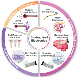 Schematic overview of emerging strategies for bio-inspired electronics and neural interfaces
| Neural Interfaces and “Living Electrodes”. From simple deep brain stimulation, we are moving towards Biohybrid Neural Interfaces that use tissue-engineered axons to bridge the gap between a computer chip and the motor cortex. By “growing” biological wires into the brain, these devices achieve a level of chronic stability that allows paralysed patients to control robotic limbs with the same fluid precision as a biological arm.
Soft Bio-Sensing Wearables: Modern-day wearables have moved from the wrist to the skin. “Electronic skin” (e-skin) patches—ultrathin, breathable, and biocompatible—now monitor biochemical markers in sweat, such as cortisol and glucose, in real-time. These devices utilise MXenes and Graphene to detect molecular changes at concentrations previously only reachable via blood draws. |
| Closed-Loop Bioelectronic Medicine: The concept of “electroceuticals” is now a clinical reality. Small, biocompatible devices implanted on the vagus nerve can monitor inflammatory markers and automatically deliver precise electrical pulses to inhibit the “cytokine storm” associated with autoimmune diseases like rheumatoid arthritis and Crohn’s disease. |
Some key challenges remain to be resolved:
Engineering Challenges:
- Stability and Bio-Integration
Despite the progress, engineering the interface remains a complex task. The physiological environment is incredibly harsh—warm, salty, and chemically active—leading to the degradation of many synthetic materials.
- Hermetic Packaging vs. Biocompatibility
Engineers must find a critical balance between the need to seal sensitive electronics from moisture while ensuring the outer layer is soft enough to integrate with tissue. In 2026, atomic layer deposition (ALD) is used to create nanometer-thin ceramic coatings that provide moisture barriers without adding stiffness.
- The Power Problem
Traditional batteries are bulky and toxic. Next-generation devices are increasingly powered by biofuel cells that harvest energy from blood glucose or through ultrasonic power transfer, which allows deep-seated implants to be recharged wirelessly through layers of muscle and bone
Ethics and the Regulatory Challenges
- As we successfully integrate electronics into the human body, the ethical implications have shifted from “safety” to “agency and privacy.”
- The EU Medical Device Regulation (MDR) and the FDA’s Digital Health Centre of Excellence have established new frameworks for “Neural Data Privacy.”Since these devices can read and potentially influence neural states, the data they produce is classified as a biological asset.
- Furthermore, the longevity of these devices raises questions about “hardware obsolescence” in living patients. Engineering the interface now includes a roadmap for software updates and long-term support for implants that may stay in the body for decades.
The Future: Toward “Living” Bioelectronics
The trend is moving toward synthetic biology-electronics hybrids. We are seeing the prototypes of devices where genetically engineered cells that produce an electrical signal work as “Sensors” when they detect a specific pathogen or cancer marker.
By engineering the interface at the molecular level, we are not just repairing the body; we are enhancing its resilience.
The integration of electronics into biocompatible materials is more than a technical achievement—it is the foundation of a new era of personalised medicine where the device and the patient are the same.
The post Engineering the Interface: Integrating Electronics into Biocompatible Materials for Next-Generation Medical Devices appeared first on ELE Times.
EU–India FTA: A Defining Moment for India’s Electronics and Semiconductor Industry
As global electronics and semiconductor supply chains are restructured for resilience and trust, the proposed EU–India Free Trade Agreement (FTA) is emerging as a pivotal opportunity for the Indian industry. More than a tariff-reduction exercise, the agreement has the potential to integrate India more deeply into Europe’s advanced electronics and semiconductor value chains. For India, the FTA represents a transition—from cost-driven manufacturing to value-driven, technology-led partnership.
The European Union is one of the world’s most quality-conscious electronics markets, with strong demand across automotive electronics, industrial automation, medical devices, power electronics, renewable energy systems, and telecom infrastructure. Under the EU–India FTA, reduced tariffs and streamlined regulatory frameworks will enhance the competitiveness of Indian electronics products.
Alignment on conformity assessment and technical standards will shorten qualification cycles and lower compliance costs, enabling Indian manufacturers to integrate directly into EU OEM and Tier-1 supply chains. As European companies pursue China-plus-one sourcing strategies, India stands to gain as a reliable and scalable manufacturing base.
India’s electronics industry has historically been assembly-led, but this is changing rapidly. Supported by policy incentives and growing design capabilities, Indian firms are expanding into PCB assembly, system integration, testing, and engineering services.
The EU–India FTA accelerates this shift by encouraging European OEMs to localise higher-value activities in India. Electronics manufacturing services (EMS) providers, component manufacturers, and design-led companies can leverage European partnerships to move beyond box build toward design-for-manufacturing, reliability engineering, and lifecycle management—key to long-term competitiveness.
Semiconductors are central to the EU–India technology partnership. The FTA aligns closely with India’s Semiconductor Mission and the EU Chips Act, creating a stable framework for collaboration across design, packaging, testing, and advanced manufacturing.
India’s strengths in chip design, embedded systems, and engineering talent complement Europe’s leadership in semiconductor equipment, materials, power electronics, and automotive-grade chips. Reduced barriers for capital equipment, technology transfer, and skilled workforce mobility can accelerate joint investments in OSAT, ATMP, and speciality semiconductor manufacturing.
This collaboration positions India as a trusted node in Europe’s semiconductor supply chain diversification efforts.
Beyond large fabs and design houses, the FTA creates opportunities for component and equipment suppliers. Demand for sensors, power modules, passive components, connectors, precision tooling, and clean-room equipment is expected to rise as European electronics and semiconductor companies expand operations in India.
Indian MSMEs operating in these segments can integrate into European Tier-2 and Tier-3 supply chains, benefiting from long-term sourcing contracts, technology upgrades, and exposure to global quality benchmarks.
The EU–India FTA also strengthens innovation linkages. Indian start-ups working in semiconductor IP, AI-enabled hardware, EV electronics, power electronics, and Industry 4.0 solutions will gain improved access to European R&D ecosystems, pilot customers, and funding platforms.
Europe’s strong IP regimes and industrial testbeds offer Indian deep-tech start-ups a credible pathway from development to global commercialisation.
Alignment with European technical, safety, and environmental standards will enhance the global credibility of Indian electronics and semiconductor products. Standards convergence reduces certification duplication, improves supplier trust, and increases acceptance across multiple export markets. For global buyers, this translates into confidence in Indian suppliers—an essential requirement in electronics and semiconductor sourcing.
The EU–India FTA arrives at a defining moment for the electronics and semiconductor industry. With effective execution, it can accelerate India’s shift from assembly-led operations to value-added manufacturing, design, and innovation. More importantly, it positions India as a strategic, trusted partner in global electronics and semiconductor supply chains—built on quality, resilience, and long-term collaboration.
Devendra Kumar
Editor
The post EU–India FTA: A Defining Moment for India’s Electronics and Semiconductor Industry appeared first on ELE Times.
Making my first circuit with a breadboard.
 | I’m really excited to try some circuits and build a decimal to binary/hexadecimal game. I’m in school for automation and robots, smart manufacturing and industrial technology, so I have a base knowledge of how circuits work. I’ve never used a breadboard, we mostly wire up components to make a complete circuit, more so electrician work. I also got a solder iron recently. I’m really excited and wanted to share. I’ll definitely be back to show the finished project. The breadboard is smaller but I’m sure it’s enough for a beginner. For the most part, I know what the included parts are for. I am excited to get into this! [link] [comments] |
Pages


![[link]](https://i.redd.it/2griqc30k9hg1.jpeg)