
Feed aggregator
Inter-die gapfill tool claims advanced packaging breakthrough

A new inter-die gapfill tool is purpose-built to solve critical challenges in 3D stacking and high-density heterogeneous integration. VECTOR TEOS 3D provides ultra-thick, uniform inter-die gapfill by leveraging Lam Research’s proprietary bowed wafer handling approach and advancements in dielectric deposition.
Industry watchers describe it as a significant step for advanced packaging, as void-free, nanoscale gapfill could be crucial for reliable 3D stacking and chiplet integration in next-generation artificial intelligence (AI) and high-performance computing (HPC) semiconductor devices.
The semiconductor industry is turning to 3D advanced packaging to integrate multiple dies into chiplet architectures for AI, HPC, and gaming applications. These chiplet designs enhance processing speed and pack more compute into smaller form factors by bringing memory and processing closer, thereby optimizing electrical pathways.
However, as these chipsets scale taller and become more complex, they encounter a range of new manufacturing challenges. That spans from stress during processing—which can distort or bow a wafer’s shape—to cracks and voids in films that cause defects and lower yield. In other words, when chip designers scale devices vertically and horizontally, they require a dielectric gapfill that is thick enough to fill the spaces between stacked dies for structural, thermal, and mechanical integrity.
It’s interesting to note that progress in modern chips is traditionally measured by development of thinner and smaller structures. On the other hand, advanced packaging strays from this convention, seeking ways to make films thicker as they stack dies higher and higher. Here, thick wafers and their associated glass substrates respond differently to thermal cycles, contributing to bowing. And handling bowed wafers is notoriously difficult.
Inter-die gapfill tool
Enter VECTOR TEOS 3D (pronounced “TEE-oss”), Lam Research’s deposition tool specifically designed for advanced packaging to reliably deliver ultra-thick films—dielectric gapfill films up to 60-µm in thickness—and thus excel at processing thick wafers with high bowing characteristics. TEOS minimizes cracks and voids in thick dielectric gapfill films while handling high-bow wafers.

Figure 1 TEOS 3D provides high-quality, void-free thick dielectric film deposition for advanced packaging. Source: Lam Research
Film cracks and voids can damage finished dies, each worth tens of thousands of dollars. “VECTOR TEOS 3D deposits the industry’s thickest, void-free, inter-die gapfill films, customized to meet the challenging requirements of advanced die stacking integration schemes, even on ultra-stressed, high-bow wafers,” said Sesha Varadarajan, senior VP of the Global Products Group at Lam Research.
TEOS deposits specialized dielectric films of up to 60 microns thick between dies with nanoscale precision, though it provides scalability to deposit films greater than 100 microns. These films provide essential structural, thermal and mechanical support to prevent common packaging failures such as delamination.
Next, TEOS features Lam’s novel clamping technology and an optimal pedestal design, offering exceptional stability when processing thick wafers. That, in turn, facilitates uniform film deposition even when dealing with extreme wafer bow.
Finally, Lam’s quad station module (QSM) architecture features four distinct stations, enabling parallel processing and reducing bottlenecks. It leads to nearly 70% faster tool throughput compared to Lam’s previous generation of gapfill solutions. Moreover, the high throughput resulting from the modular design helps improve the cost of ownership up to 20%.

Figure 2 TEOS addresses a range of advanced packaging challenges. Source: Lam Research
Other key features of TEOS include a large chamber design, ringless wafer transfer, and integrated equipment intelligence.
Why it matters
Advanced packaging is now an essential part in the development of next-generation chips such as GPUs and HBM memory chips. The GPU/HBM stacks are growing more complex while packing in more transistors. Therefore, traditional solutions are increasingly falling short.
Advanced packaging requires extreme precision at every step of the chipmaking process, spanning from plating to etch. Lam claims that TEOS is the first solution for single-pass processing of crack-free films exceeding 30 microns in thickness. That significantly enhances yield and process time.
TEOS is now installed at leading logic and memory fabs around the world.
Related Content
- Will 2024 be the year of advanced packaging?
- One-stop advanced packaging solutions for chiplets
- Intel’s Embarrassment of Riches: Advanced Packaging
- Nvidia, TSMC, and advanced packaging realignment in 2025
- Understanding the Big Spend on Advanced Packaging Facilities
The post Inter-die gapfill tool claims advanced packaging breakthrough appeared first on EDN.
Back when resistors and capacitors had personality
 | Pulled apart an old valve amp and was struck by how good the color-coded caps and resistors looked. Modern SMD boards just feel boring in comparison. Anyone else miss this aesthetic? [link] [comments] |
Old vs New Enclosure
 | Only two components, a esp32 board & 0.96 inch oled screen, blue is the 0.96 inch oled screen & black is the esp32 with USB-C [link] [comments] |
Understanding Varactor and PLL-Based FM Generation Using Crystal Oscillators
Analog Electronics: The Timeless Backbone of Modern Sensors
Introduction: The “Old” Tech Powering the “New” World
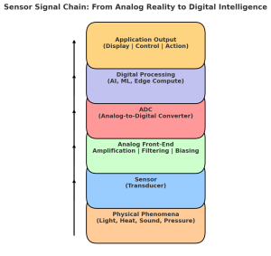
In today’s electronics ecosystem, conversations are dominated by artificial intelligence, edge computing, and ultra-fast wireless networks. Yet, behind every groundbreaking innovation, there lies a quieter but indispensable player i.e., analog electronics. While digital may dominate headlines, it is analog that ensures real-world phenomena which can be captured, conditioned, and processed.
As engineers often remind themselves, “Nature is analog. Everything else is an approximation.” No matter how sophisticated a digital system is, its accuracy and reliability hinge on the quality of the analog front-end. From radar in advanced driver-assistance systems (ADAS) to MEMS accelerometers in smartphones, and from biomedical wearables to industrial IoT nodes, analog electronics forms the first link in the sensor signal chain.
Why All Sensors Speak Analog First
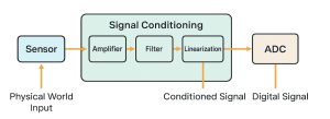
Every physical phenomenon light intensity, sound waves, heat, vibration, or radio frequency (RF) radiation exists in analog form. Sensors are essentially transducers, converting these continuous signals into measurable electrical quantities. But before such data can be digitized and analyzed by processors or AI algorithms, it must pass through an analog front-end (AFE).
The AFE includes key blocks such as instrumentation amplifiers, filters, linearization circuits, and signal conditioning modules that prepare raw sensor outputs for analog-to-digital conversion (ADC). Without robust analog conditioning, even the most advanced digital processors would be “blind” to the real world.
As Walt Maclay, CEO of Voler Systems, puts it: “Digital processing is only as good as the analog electronics feeding it. Garbage in, garbage out applies more to sensors than anywhere else.”
Core Functions of Analog in Modern Sensors
- Signal Amplification
Many sensors output signals in the microvolt or millivolt range, easily drowned by noise. Instrumentation amplifiers and low-noise amplifiers (LNAs) boost these signals while preserving fidelity. For example, electrocardiogram (ECG) sensors require amplifiers with high common-mode rejection ratios (CMRR) to extract meaningful heart signals from noise-laden environments. - Filtering
Real-world signals are messy. Analog active and passive filters remove unwanted noise and interference before digitization. In radar systems, bandpass filters ensure only the target frequency range is processed, dramatically improving signal-to-noise ratio (SNR). - Linearization & Biasing
Many sensor outputs are nonlinear by nature. Analog circuits implement linearization techniques that correct these distortions, making sensor behavior predictable. Similarly, biasing ensures transducers operate in optimal ranges. For example, in thermistors, resistance-to-temperature curves must be linearized before meaningful temperature data is derived. - Conversion Readiness
Analog circuits prepare signals for ADC compatibility by ensuring proper voltage levels, impedance matching, and bandwidth. Without this step, digitization could lead to clipping, aliasing, or resolution loss.
Case Studies: Analog at Work in Emerging Applications
- Automotive ADAS
ADAS relies heavily on radar and LiDAR sensors, where real-time performance is non-negotiable. Analog front-ends amplify weak RF echoes, filter them for interference, and feed precise signals to high-speed ADCs. Even a microsecond delay can mean the difference between safe braking and a collision.
- Biomedical Devices
Wearable medical devices like glucose monitors and ECG patches demand ultra-low-power, high-precision analog circuits. Here, analog electronics extend battery life while ensuring clinical-grade accuracy. An error of even 1 mV in amplification could translate into misdiagnosis.
- Industrial IoT
Factories rely on thousands of sensors for vibration monitoring, predictive maintenance, and process automation. Analog circuits in these environments must withstand electrical noise, temperature fluctuations, and mechanical stress. Unlike fragile digital logic, robust analog designs ensure reliability under extreme industrial conditions.
- Environmental Monitoring
Long-term stability is critical in air-quality monitors, soil sensors, or weather stations. Analog circuits designed for low drift and high linearity guarantee consistent data for years without recalibration.
Analog’s Edge Over Digital in Certain Tasks
While digital processing offers flexibility, analog holds an edge in critical aspects:
- Zero Latency: Analog signals propagate at the speed of physics — no clock cycles required. For radar-based collision avoidance, this deterministic performance is irreplaceable.
- Power Efficiency: Analog front-ends consume far less power than equivalent digital circuits, making them essential in wearables and IoT nodes where every microamp counts.
- Reliability under Harsh Conditions: Analog circuits continue functioning in extreme environments — radiation, high temperatures, or electromagnetic interference — where digital logic often fails.
As Bob Dobkin, co-founder of Linear Technology, famously said: “Analog will never die, because the world is analog.”
Integration Trends: Analog in the Age of SoCs and SiPs
The industry is increasingly moving towards system-on-chips (SoCs) and system-in-packages (SiPs) that integrate both analog and digital functions. For instance, today’s MEMS inertial sensors often include on-chip AFEs, ADCs, and digital processors in a single package. This integration reduces footprint, improves signal integrity, and supports miniaturization for wearables, drones, and autonomous systems.
However, integration does not eliminate the need for analog expertise. Instead, it requires engineers to design mixed-signal systems where the interplay between analog and digital domains is carefully managed. Issues like thermal drift, bandwidth matching, and parasitic effects remain squarely in the analog domain.
Conclusion: Analog as the Permanent Foundation
In the race towards digital transformation, analog electronics is often overlooked. Yet, it is precisely analog that determines how effectively digital systems can sense and respond to the physical world. Whether in self-driving cars, medical diagnostics, or industrial automation, analog remains the timeless backbone of modern sensors.
For engineers, the message is clear: mastering analog design is not a relic skill, but a future-proof investment. The more complex and interconnected systems become, the more critical it is to ensure rock-solid analog foundations.
As the electronics pioneer Barrie Gilbert once noted: “You can digitize data, but you cannot digitize reality. Reality is, and will always be, analog.”
The post Analog Electronics: The Timeless Backbone of Modern Sensors appeared first on ELE Times.
A 6 mosfet module I made for breadboard use
 | I was playing with 12v LED cob panels and wanted to drive them from a esp32 on breadboard. So i made this, with 6 2N7000 mosfets and the associated resistors. I was quite pleased with my happy notion of alternating the orientation of the transitors alternately so the sources were all in a line, this also made the drains form neat pairs. which was nice. [link] [comments] |
Very simple TCI ignition system
 | Hello everyone, Chris here. I built a simple TCI ignition module, and it works— but I haven’t tested it yet on a motorcycle or anything else. My friend said he had done this before on a classic car and it worked. I’ve uploaded a full tutorial video with the circuit and parts on YouTube. You can check it out and let me know what you think— I’ll put the link in the comments. [link] [comments] |
Third party (non-AIB) Video card pcb with its chip removed
 Video card pcb with its chip removed") | submitted by /u/computune [link] [comments] |
Weekly discussion, complaint, and rant thread
Open to anything, including discussions, complaints, and rants.
Sub rules do not apply, so don't bother reporting incivility, off-topic, or spam.
Reddit-wide rules do apply.
To see the newest posts, sort the comments by "new" (instead of "best" or "top").
[link] [comments]
Freehand Pcb creation with 555 flasher.
 | I want to make my own PCBs, but i find all the PCB design programs infuriating. So i have been honing my free hand skills, using blank copper clad board and an etch resistant pen. This, a simple 555 flasher, is my latest one. I used a SOIC 555 with 0805, and 0603 surface mount supporting components. [link] [comments] |
Generative Artificial Intelligence Boosts Chip Yields and Slashes Manufacturing Defects
In 2021, car manufacturers worldwide halted production because a single one-dollar microcontroller was unavailable. The wait time for advanced semiconductors jumped from 12 weeks to over 26 weeks, revealing how fragile the global supply chain had become. The yield losses and manufacturing defects are not just technical issues-they are strategic challenges affecting procurement leaders, supply chain managers, and even national economies.
Meanwhile, demand for semiconductors continues to grow relentlessly. Global consumption is expected to increase at a compound annual growth rate of 7 to 8 percent through 2030, while production capacity is only growing at about 5 percent per year. This mismatch makes every wafer incredibly valuable. Even a modest 2 percent improvement in yields at advanced technology nodes could free up around 150,000 wafers annually, which translates into billions of dollars of extra supply.
Generative AI addresses these challenges by creating optimized designs in advance, anticipating potential defects, and enhancing scheduling in wafer fabrication. It is reshaping the economics of the semiconductor industry- improving yields, reducing inconsistencies, and strengthening supply chains’ reliability.
The Yield Challenge in Semiconductor Manufacturing
Chip manufacturing involves more than 1,000 steps, from photolithography to etching. At advanced nodes of three nanometres and below, tiny atomic-level variations can make wafers unusable. With single-wafer costing over 16,000 dollars, any loss in yield directly cuts profit margins.
Every percentage point of yield improvement is like adding a new fabrication plant without capital investment, said Sanjay Mehrotra, CEO of Micron Technology.
How Generative AI Creates Strategic Value
Generative models such as Generative Adversarial Networks (GANs), Variational Autoencoders (VAEs), and foundation models go beyond predictive analytics: they generate better alternatives. Four applications stand out:
- Design Optimization
Generative AI evaluates thousands of layout variations to identify configurations that reduce defects. Synopsys, working with Taiwan Semiconductor Manufacturing Company (TSMC), reported a 15 percent yield improvement using AI-driven design space exploration. Faster design cycles and quicker delivery to customers follow. A European fabless design company leveraged generative AI for design optimisation and achieved ROI in just 18 months, reducing wafer scrap, accelerating revenue realization, and lowering operational costs.
- Defect Prediction
AI generates synthetic wafer maps to train inspection systems before defects appear. American-based KLA corporation reported 25–30 percent improvement in defect detection, resulting in more usable wafers and faster production cycles. Samsung implemented AI-based yield learning to cut line failure rates by 12 percent, decreasing buffer inventory needs and improving delivery reliability.
- Assistance with Lithography
AI supports mask patterns generation to minimize distortions through Inverse Lithography Technology (ILT) and Optical Proximity Correction (OPC). Intel reported a 40 percent reduction in edge-placement error, increasing first-pass yields.
- Supply Assurance and Fabric Scheduling
Generative AI simulates thousands of scheduling scenarios, balancing tool usage, and maximizes throughput. A Taiwanese fabless company reduced wafer cycle times from 20 to 17 days using AI scheduling, ensuring timely chip delivery in a competitive market.
It also strengthened broader supply chain resilience. Global Foundries applied predictive analytics to reduce recovery times during material shortages by 30 percent, helping procurement meet client demand during disruptions.
Industry Case Studies and Outcomes
- Samsung Foundry – AI-based Yield Learning- It reduced the cut line failure rates by 12 percent, lowering buffer inventory requirements and improving delivery reliability for customers.
- Global Foundries – Predictive Supply Chain Analytics: Using predictive analytics, it improves supply chain resilience and cuts recovery times during material shortages by 3 percent, enabling procurement teams to meet client demands.
- European Fabless Design Company – Design Optimisation: Employing generative AI for layout optimisation, the company achieved return on investment (ROI) in just 18 months. By decreasing wafer scrap, speeding revenue realisation, and reducing operational cost.
Strategic Procurement and Supply Chain Value
Generative AI serves the dual role. On the shop floor, it functions like examining billions of flaw patterns to increase yields. In the boardroom, it mitigates risk, strengthens supply continuity, and protects margin.
Predictive insight facilities by generative AI can help with lead time optimisation, multi-sourcing strategy guidance, and supplier negotiations, and align contractual requirements with actual fab performance, ensuring reliable capacity guarantees.
SEMI CEO Ajit Manocha stated that generative AI is not just yield enhancement-, it lowers process variability, increases predictability, and strengthens overall operational resilience.
Challenges to Adoption
Despite its transformative potential, adopting generative AI in the semiconductor industry presents several challenges:
Ø Data confidentiality: It remains the key concern because the processed data is so proprietary and difficult to share across ecosystems.
Ø Computational intensity: It requires a substantial amount of computational equipment to train sophisticated AI generative models.
Ø Explainability gaps: To foster confidence, engineers and procurement teams need AI advice to be transparent.
Ø Change management: To fully realise value, Fabs must retrain process engineers, educate procurement specialists in AI literacy, and link data science teams across silos.
The Road Ahead: Toward Autonomous and Resilient Fabs
Next-generation semiconductor factories are increasingly relying on generative AI as central intelligence. Emerging trends include:
- Autonomous fabs: It leverages generative AI to modify recipes in real time to reduce yield loss and improve efficiency.
- Collaborative ecosystems: Design firms, equipment manufacturers, and fabs share AI models to optimize production and supply chain resilience.
- Zero-defect manufacturing: While idealistic, generative AI is making substantial progress towards achieving it, bringing fabs closer to near-perfect yield and consistency.
Strategic Imperatives for Leaders
The path forward is clear for procurement executives, semiconductor leaders, and strategy decision makers:
- Scale AI across operations: Transition from pilots to full integration in scheduling, lithography, electronic design automation, and inspection workflow.
- Leverage AI in procurement: Use insights for contract negotiations, supplier diversification, and lead time predictability.
- Invest in people and collaborations: Integrate the expertise of supply chain managers, data scientists, and strengthen collaboration with AI solution providers and academic institutions.
Conclusion
Generative AI is transforming chip manufacturing. It boosts yields, cuts defects, and improves production scheduling. More importantly, it helps leaders make supply chains stronger, margins steadier, and delivery times more predictable.
Companies that embrace AI first will unlock extra capacity, protect supply continuity, and gain a clear competitive edge. Every wafer counts, and every week of lead time matters. Generative AI ensures neither is wasted.
The post Generative Artificial Intelligence Boosts Chip Yields and Slashes Manufacturing Defects appeared first on ELE Times.
Доповідь ректора КПІ ім. Ігоря Сікорського Анатолія Мельниченка на сесії професорсько-викладацького складу 29 серпня 2025 року

Шановні учасники та гості сесії професорсько-викладацького складу університету, дозвольте привітати вас з 34-ю річницею незалежності України та 127-ю річницею від дня заснування КПІ!
💛💙
NREL’s silicon carbide-based ULIS power module claims record efficiency, power density, and low-cost manufacturability
Apple’s 2H 2025 announcements: Tariff-touched but not bound, at least for this round

On Tuesday, Apple, as usual for a September, unveiled its latest-generation tranche of iPhones, Apple Watches, wireless headphones, and the like, at its as-usual-prerecorded “Awe Inspiring” event (here’s last year’s event coverage from yours truly, if a preparatory memory refresh is necessary). Admittedly, there wasn’t anything terribly surprising unveiled, in no small part because much of it was predictable (last year’s iPhone 16 series was superseded by this year’s 17 series, for example…duh…) and a lot of it was also inevitable, “thanks” to the usual internal, partner (case suppliers and cellular carriers, for example) and supply chain players’ in-advance leaks. Never fear, however: I still found plenty of interesting (at least to me) tidbits big-and-small that I’ll be sharing in the following sections.
The chipsI’ll start with what the engineers out there are most interested in: the new phones’ internals. Much as the generational number-naming cadence for the new phones (three of them, at least: hold that thought) was predictable, so too is the cadence for their SoCs: last year’s A18 processors have been superseded by A19s (again…duh). And as usual, we don’t have a lot of details on them—clock speeds, cache size specifics, etc.—although Geekbench benchmarks on the “Pro” variant are already published. So, what do we know? Here’s the baseline A19, with a CPU cluster comprised of two performance and four efficiency cores, and a five-core GPU:


And here’s what Apple says about it:
Built on third-generation 3-nanometer technology, A19 delivers powerful performance, efficiency, and a huge boost in speed. An updated display engine, ISP, and Apple Neural Engine power features like Apple Intelligence and the latest-generation Photographic Styles. The 6-core CPU is 1.5x faster than the A15 Bionic chip in iPhone 13, and the 5-core GPU is more than 2x faster than A15 Bionic, unlocking stunning graphics and next-level mobile gaming. Neural Accelerators are also built into each GPU core to help run powerful generative AI models on device.
 For comparison’s sake, the A18 was also a two-performance-core/four-efficiency-core CPU cluster architecture, with GPU core counts from four to six depending on the target device, albeit “binned” during test from the exact same originating sliver of silicon, I ‘spect.
Now for the A19 Pro:
 Same two-performance-core/four-efficiency-core CPU cluster architecture as the baseline A19. So, what’s the “diff”? Apple claims that the “Pro” performance cores have both enhanced branch prediction and front-end bandwidth, and the new efficiency cores have more “last-level” (likely translation: core-shared) cache: a 50% capacity boost, to be precise. Now for the GPU:


Two graphics cluster options, at least so far: 5- and 6-core counts. Stay tuned for which phone(s) each goes into. And here’s what Apple says about the A19 Pro:
A19 Pro is Apple’s most capable iPhone chip yet. When paired with the Apple-designed vapor chamber, A19 Pro enables iPhone 17 Pro and iPhone 17 Pro Max to deliver up to 40 percent better sustained performance than the previous generation — ideal for gaming, video editing, and running large local language models. The 6-core CPU is the fastest CPU in any smartphone, and the 6-core GPU architecture includes Neural Accelerators built into each GPU core, a larger cache, and more memory than A18 Pro. The GPU works in tandem with the new 16-core Neural Engine to power Al models, stunning graphics, and AAA gaming titles like Arknights: Endfield, enabling hardware-accelerated ray tracing and higher frame rates.
Following both Apple-authored paragraphs I’ve already shared is another one, revealing another IC, this one more revolutionary versus evolutionary, although the concept’s already proven:
The iPhone 17 lineup also introduces N1, a new Apple-designed wireless networking chip that enables Wi-Fi 7, Bluetooth 6, and Thread. In addition to powering the latest generation of wireless technologies, N1 improves the overall performance and reliability of features like Personal Hotspot and AirDrop.

Apple has long stated its aspiration to “own” as much of the silicon foundation of its products as possible—with the likely exclusion of DRAM and flash memory, along with image sensors—although long-term on that last one, who knows? Broadcom had historically been Apple’s predominant supplier of wireless networking technology, although Apple had already ventured out on its own with earbuds (Bluetooth) and smart watches (both Bluetooth and Wi-Fi). That said, and perhaps obviously, the N1, whose development was rumored back in December, is a notable advancement on this foundation from both performance and functionality standpoints, including the welcome inclusion of Matter-related Thread support.
And speaking of wireless connectivity, what about the cellular side of the family? Apple’s iPhone 16e, introduced earlier this year, had first-time included the company’s in-house-developed cellular subsystem, the C1. Now there’s the C1X successor:
C1X, a new cellular modem designed by Apple…is up to 2x faster than C1, and for the same cellular technologies, it is even faster than the modem in iPhone 16 Pro, while using 30 percent less energy overall. This makes C1X the most power-efficient modem in an iPhone.

That said, the C1X is included in only one of this September’s new phones. Here’s a hint: power consumption is particularly critical with this particular mystery phone model. And the downside: as a result, it doesn’t support mmWave 5G cellular data services. Stay tuned for the details (assuming you haven’t already figured it out after visiting one of the earlier links).
One other IC-related advancement, supported by the A19 SoC series (and presumably future A-, M-, and other-series chips as well), bears mention. It’s Memory Integrity Reinforcement, which Apple describes as follows within a detailed Security Engineering and Architecture (SEAR) post:
Memory Integrity Enforcement (MIE) is the culmination of an unprecedented design and engineering effort, spanning half a decade, that combines the unique strengths of Apple silicon hardware with our advanced operating system security to provide industry-first, always-on memory safety protection across our devices — without compromising our best-in-class device performance. We believe Memory Integrity Enforcement represents the most significant upgrade to memory safety in the history of consumer operating systems…
Memory Integrity Enforcement is built on the robust foundation provided by our secure memory allocators, coupled with Enhanced Memory Tagging Extension (EMTE) in synchronous mode, and supported by extensive Tag Confidentiality Enforcement policies. MIE is built right into Apple hardware and software in all models of iPhone 17 and iPhone Air and offers unparalleled, always-on memory safety protection for our key attack surfaces including the kernel, while maintaining the power and performance that users expect.
With all due respect, SEAR might have gotten at least a bit out over its skis; conceptually similar schemes have already been implemented by Microsoft (in Windows 11) and Arm (supported, for example, by Google beginning with the Pixel 8 series). That said, as The Verge notes:
Apple says its implementation goes a step further, with the ability to protect all users by default and by designing its A19 and A19 Pro chips for enhanced security, while still adding memory safety changes for older hardware that doesn’t support the new memory tagging features. The company also says its new mitigation for Spectre V1 leaks works with “virtually zero CPU cost” — as performance hits have been an issue for memory integrity and other security features — with all of the changes making “mercenary spyware” even more expensive to develop.
Time will tell, I suppose.
The iPhone 17s (iPhone 17)

(iPhone 17 Pro Series)
Nearly 1,500 words in, and I haven’t even gotten to the products themselves yet? Oh, bother. Let’s speed things along for the remainder of this piece by switching to bullets where possible:
- There are three of them this time: the baseline iPhone 17, the high-end iPhone 17 Pro, and the Pro Max.
- The iPhone 17 runs the baseline A19 SoC, while both “Pro” models embed the six-GPU-core variant of the A19 Pro.
- iPhone 17 capacities start at 256 GBytes, for the same $799 price tag that the 128 GByte iPhone 16 sold for a year ago. That same 128 GByte iPhone 16, now selling for $100 less ($699), is the only capacity variant of that particular 16th-generation model still offered by Apple for purchase (along with both 128 GByte and 256 GByte versions of the iPhone 16 Plus, interestingly, as well as the more recently introduced iPhone 16e, of course). And of course, the iPhone 15s have been expunged from the company’s product line.
- Turn to the Pro variants, and things get even more interesting. Again, there’s no 128 GByte 17th-generation option. But no iPhone 16 Pros (or Pro Maxes, for that matter) are being sold any longer, either, so $1,099 (in fairness, matching what the 256 GByte iPhone 16 sold for a year ago) is now your lowest-priced 17 Pro entry point (therein explaining the “touched by tariffs” nuance in this post’s title). And hey, if you’ve got $2,000+ sitting around begging to be burned, you could instead spend it on a 2 TByte iPhone 17 Pro Max…
- I find this quite interesting; all three phones are sold in both physical SIM (only in some countries) and eSIM-only options. What did Apple do with the internal space freed up by the removal of the physical SIM tray and other hardware bits? They instead devoted it to higher-capacity batteries, at least for Pro models; eSIM-only phones spec longer between-charges operating life.
- In today’s example of “insincere feature set restrictions in order to encourage purchase upgrades”, the USB-C port on the iPhone 17 only runs at USB2-compatible 480 Mbps data transfer rate speeds. Should you wish to shoot video on one of them, you’ll quickly run out of internal storage and then realize that the tethered external-storage bandwidth isn’t up to snuff, either…or you could just proactively buy an iPhone Pro model instead. And before you point to the A19-vs-A19 Pro differentiation as the root cause…the other just-released iPhone (which I’ll discuss next) is A19 Pro-based, but is USB2-only, too.
- Speaking of video (and image capture more generally); both rear cameras on the iPhone 17 now have 48 Mpixel image sensors (vs 12 Mpixels for the ultrawide in the iPhone 16). The same goes for the three cameras on the Pro models (on the 16th generation predecessors, the telephoto was 12 Mpixels). And all three models’ front cameras not only bump up the resolution from 12 Mpixels to 16 Mpixels but also support Center Stage AI-enabled algorithms that dynamically crop and interpolate to keep subjects centered in the frame.
- The displays are now protected by next-generation Ceramic Shield 2 coatings; the back panel on Pro models now has prior-generation Ceramic Shield protection, too. As for sizes and such, the iPhone 17 makes the biggest jumps; from 6.1” diagonal to 6.3” (along with generationally shrunken bezels), now also supporting dynamically switching (to optimize for at-the-moment application need vs battery life, which Apple brands as ProMotion) refresh rates up to 120 Hz (and down to 1 Hz).
- The Pro devices’ frames are now once again aluminum-fabricated, fundamentally (presumably) to simplify the fabrication process and otherwise reduce cost (of the raw material, along with allowing for reuse of scrap) vs titanium. Tariffs strike again…
- And whereas the baseline iPhone 17 RAM capacity is generationally unchanged at 8 GBytes, the Pro variants bump it from 8 to 12 (reportedly) GBytes. AI strikes again…
- Oddly, there’s no black (or near-black) color option offered for either of the Pro models
- All three models continue to rely on Qualcomm cellular subsystems, presumably (if for no other reason) to afford them with optional mmWave 5G support.
- And last, but not least: does that new backside-spanning “camera bar” arrangement for the iPhone 17 Pro models remind you at least somewhat of a Google Pixel, or what?
![]()
Apple sells “Air” laptops. And “Air” iPads. So, you had to know an “Air”-monicker iPhone was going to arrive sooner or later, right? Right.

A quick aside, once again with the big-picture theme of tariff-counteracting moves to preserve profits. Keen-eyed readers might have noticed that there’s no 6.7″ “Plus” iPhone version in this generation. Granted, the baseline iPhone 17 display is a smidge bigger than it was before, as already noted. But want something brand-new and even bigger, and you’ll need to jump all the way up to the $1,199-or-higher 6.9” iPhone 17 Pro Max…or make a lateral move instead, to the $999-or-more 6.5” iPhone Air.
What do you get for paying $200 more than a baseline iPhone 17 of the same capacity?
- The aforementioned slightly larger display
- The aforementioned more powerful CPU (although this version of the A19 Pro is only “binned” for five active GPU cores, and I’m betting it’s also comparatively underclocked for thermal and battery life reasons)
- A 1 TByte capacity option (for “only” $1,399)
- 09 inches/2.16mm less thickness (0.34 inch/8.75 mm for the iPhone Air, versus 0.31 inch/7.80 mm for the iPhone 17)
- 42 ounces/12 grams less weight (5.82 ounces/165 grams for the iPhone Air, versus 6.24 ounces/177 grams for the iPhone 17)
- And a titanium-based frame. Apple apparently was loath to have another “Bendgate” on its hands…bad pun intended:
And what do you lose, beyond an extra $200? Well…
- A second backside camera
- mmWave 5G cellular data connectivity (this is the “mystery model” mentioned earlier, based on Apple’s C1X chip, if you hadn’t already figured it out)
- Battery life: a 3,149 mAh battery for the iPhone Air, not counting the $99 Air-only MagSafe external battery, versus 3,692 mAh for the iPhone 17
- Slower charging speeds: 20W-max MagSafe and USB-C charging on the iPhone Air, again presumably due to thermal concerns, versus 25W MagSafe and 40W (60W burst) USB-C charging on the iPhone 17
- A physical SIM option, at least in some countries (the iPhone Air is eSIM-only, to squeeze as much battery capacity inside as possible for operating life reasons, presumably)
- And no “17” generational qualifier
 (which makes me wonder just what the company will call the next one?)
But hey, just like the iPhone 17, the iPhone Air also supports only USB2 480 Mbps-max wired data transfer rates (as I hinted at earlier), so…sigh.
The Apple Watches
(Apple SE 3)

(Apple Series 11)

(Apple Watch Ultra 3)
Nearing 2,500 words. Oh, d-d-d-dear! Apple’s newest-generation watches are modest-at-best upticks from their precursors, truthfully. The SE 3 and Ultra 3 have migrated from the S9 to S10 SoC internally…that said, it’s long been rumored that Apple’s kept its smartwatch SoCs pretty-much-to-completely identical the past few generations, only altering the name stamped on top. Befitting this potential reality, the S10 stays the same from the Series 10 to the new Series 11.
All three watches gain new health-monitoring and -analysis capabilities, which Apple admittedly, surprisingly, also plans to retrofit to recent past smartwatch generations. The entry-level SE 3 also inherits the previous mainstream-and-above-only always-on display option. At the high end, the Ultra 3 gets direct-connect satellite communications capabilities…nearly three weeks later than the notably more affordable (roughly half the price, in fact) Google Pixel Watch 4, and nearly a week behind Garmin’s also-satellite-cognizant fēnix 8 Pro. Oh, and dual-band GPS. See earlier versus-Google Pixel Watch 4 comment.
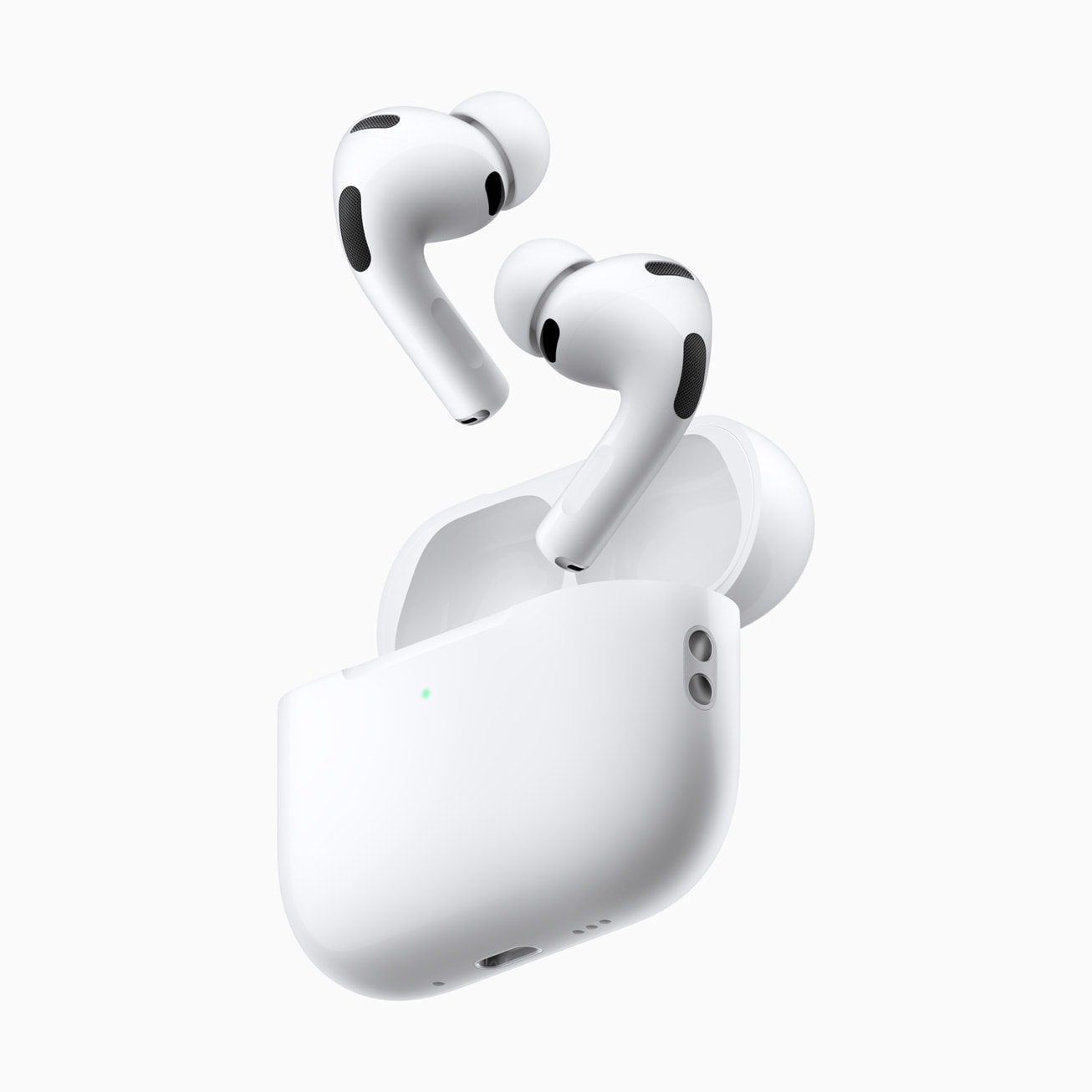
The AirPods Pro 3
Last, but not least, new-generation high-end Bluetooth earbuds (following their year-ago updated mainstream siblings). Y’know, when references to an unannounced product show up in released (albeit beta) software, my general rule of thumb is that the product won’t stay unannounced for long, capisce?
Here’s what Apple claims about the AirPods Pro 3:
AirPods Pro 3 deliver unbelievable sound quality and the world’s best in-ear Active Noise Cancellation (ANC) — removing up to 2x more noise than the previous-generation AirPods Pro, and 4x more than the original AirPods Pro.
Independent rumors and ears-on analysis admittedly back up the company’s comparative-ANC claims, but are more reserved in their audio-quality improvement assessments (then again, when I want to do critical music listening, Apple earbuds are not what I’d think to grab first…or second…or…). The H3 SoC upgrade-enabled inclusion of heart-rate detection is interesting; I just hope that lightning doesn’t strike twice, re Apple-owned Beats’ Powerbeats 2 inability to walk and chew gum at the same time (more accurately: play music while tracking heart rate on gym equipment). I mean…isn’t listening to music the fundamental point of these things?
Live language translation (and live broadcast of that translation to another AirPods set wearer) is something I very much look forward to trying out..and I will, because ever-generous Apple is backfilling the feature to the AirPods Pro 2, too (Q: Did you say AirPods Pro 2, Brian? A: Yes, I did, and genuine ones too; a story for another day). The transition from silicon to foam ear tips is interesting, too. And generally-generous Apple now includes five different-sized tip sets for optimal user fit purposes. But generosity has limits. No bundled USB-C cable (any more) for you. Have I yet mentioned tariff costs leading to counterbalancing cost reductions elsewhere?
MiscellanySpeaking of wireless earbuds, shortly before the launch event, a teaser video of Beats’ latest Powerbeats Fit appeared on Apple’s own YouTube channel:
But as I write these words, they’re not yet officially announced. My theory: Apple intentionally held them back, wanting to showcase earbuds that only work with Apple devices versus (also? Instead?) introducing ones that were cross-platform, including…insert ominous pipe organ sound…Android.
Other tidbits:
- Much as I’ve needled Apple versus Google in this writeup, I’m compelled to point out that all the products that Apple announced on Tuesday will be available for preorder on Friday, September 12, with in-store sales (and shipments) commencing the following Friday, September 19. In contrast, a notable chunk of what Google announced three weeks ago won’t be available until next month.
- Speaking of dates, the various “26” operating systems unveiled at WWDC in June will all “go gold” on Monday, September 15. That said, I’ve already got the “gold” versions of Google’s Material 3 Expressive revamps running on my Pixel phones and Pixel Watch and am lovin’ em, so….

- And one final bit of evidence of Apple’s (sometimes) generosity: the company has extended its free satellite connectivity promotion to iPhone owners for another year.
So, there you go: an as-usual mix of the impressive, the mundane, and multiple points in between. That said, who am I trying to fool? “It’s all for naught;” Apple will sell everything it’s got (yes, especially the iPhone Air). Having passed through 3,000 words a few paragraphs ago, undoubtedly spiking poor Aalyia’s blood pressure in the process, thus concludes today’s Winnie the Pooh-themed post. Let me know your thoughts in the comments!
—Brian Dipert is the Editor-in-Chief of the Edge AI and Vision Alliance, and a Senior Analyst at BDTI and Editor-in-Chief of InsideDSP, the company’s online newsletter.
Related Content
- It’s September in Apple land, so guess what it’s time for?
- The Apple iPhone 16e: No more fiscally friendly “SE” for thee (or me)
- Cracking the case of a smartphone and its unfairly crack-accused case
- If you made it through the schtick, Google’s latest products were pretty fantastic
- The 2025 WWDC: From Intel, Apple’s Nearly Free, and the New Interfaces Are…More Shiny?
The post Apple’s 2H 2025 announcements: Tariff-touched but not bound, at least for this round appeared first on EDN.
Лекція Нобелівського лауреата Сера Пола Нерса у КПІ ім. Ігоря Сікорського

11 вересня 2025 року Київська політехніка приймала візит видатного біолога, Президента Лондонського королівського товариства, лауреата Нобелівської премії з фізіології та медицини і амбасадора UNITED24 Сера Пола Нерса із лекцію «Наука як революція» у рамках V Саміту перших леді та джентельменів.
Співпраця між КПІ ім. Ігоря Сікорського та Талліннським університетом

Талліннський університет — один з найкращих закладів вищої освіти Естонії, відомим освітніми інноваціями й міждисциплінарними дослідженнями.
📌 Меморандум про співпрацю чинний до 2030 року з можливістю подовження:
Intel 1103: The DRAM Chip That Dethroned Magnetic Core Memory
EDC17CP14 V2.70 Piezo Injector driver
 | I am doing a diagnosis on some Hyundai Santa Fe D4HD. Injectors keep dying electronically every couple of minutes. Thought I might share this if anybody ever needs it... [link] [comments] |
КПІ ім. Ігоря Сікорського співпрацюватиме з провідними університетами Данії

Наш університет відвідала делегація Королівства Данії, за підсумками зустрічі з якою укладено два меморандуми про співпрацю — з Ольборзьким університетом (AAU) та Університетом Південної Данії (SDU).
Pages


![[link]](https://i.redd.it/i420ujjaw8pf1.jpeg)
![[link]](https://i.redd.it/8tdtdsobzyof1.png)
![[link]](https://i.redd.it/r9gyxbw3dqof1.jpeg)