
Збирач потоків
IQE reports strong second-half 2025 demand, driven by military & defence, AI, data center and handset markets
BluGlass secures contract extension with NCSU-led CLAWS Hub
US orders HieFo to divest Emcore indium phosphide assets
AI Glasses: Ushering in the Next Generation of Advanced Wearable Technology
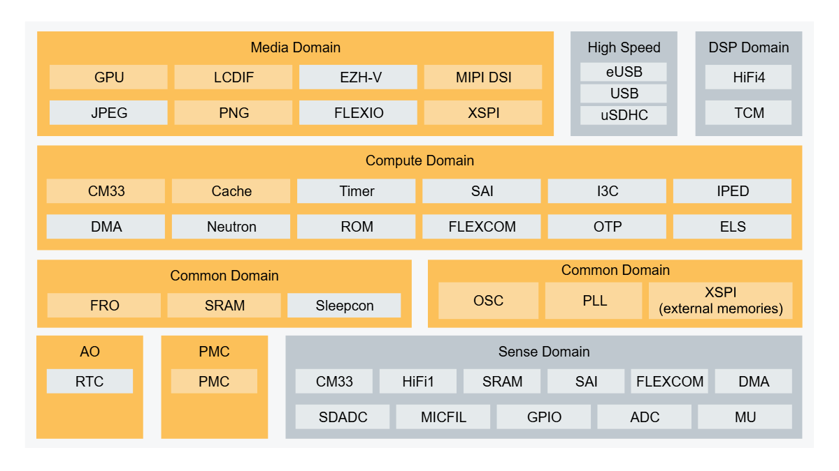
Courtesy: NXP Semiconductors
AI integration into wearable technology is experiencing explosive growth and covering a variety of application scenarios from portable assistants to health management. Their convenience of operation has also become a highlight of AI glasses. Users can easily access teleprompting, object recognition, real-time translation, navigation, health monitoring, and other operations without physically interacting with their mobile phones. AI glasses offer a plethora of use cases seamlessly integrating the digital and real worlds, powering the next emerging market.
The Power Challenge: Performance vs. Leakage
The main challenge for AI glasses is battery life. Limited by the weight and size of the device itself, AI glasses are usually equipped with a battery capacity of only 150~300mAh. To support diverse application scenarios, related high-performance application processors mostly use advanced process nodes of 6nm and below. Although the chip under this process has excellent dynamic running performance, it also brings serious leakage challenges. As the process nodes shrink, the leakage current of the silicon can increase by an order of magnitude. The contradiction between high leakage current and limited battery capacity significantly reduces the actual usage time of the product and negatively affects the user experience.
The chip architect is forced to weigh the benefits of the various process nodes, keeping in mind active power as well as leakage. With the challenge of minimising energy usage, many designs have taken advantage of a dual chip architecture, allowing for lower active power consumption by using the advanced process nodes, while achieving standby times with much lower leakage through the more established process nodes.
Solving the Power Problem: Two Mainstream Architectures
Currently, AI glasses solutions on the market mainly use two mainstream architectures:
“Application Processor + Coprocessor” Architecture
The “application processor + coprocessor” solution can bring users the richest functional experience and maximise battery life. The application processors used in AI Glasses are based on advanced processes, focusing on high performance, usually supporting high-resolution cameras, video encoding, high-performance neural network processing, and Wi-Fi/Bluetooth connectivity. In turn, coprocessors steer towards mature process technologies, focusing on lower frequencies to reduce operating and quiescent power consumption. The combination of lower active and standby power enables always-on features such as microphone beam forming and noise reduction for voice wake-up, voice calls, and music playback.
“MCU-only” Architecture
The “MCU-only” solution opens the door to designs with longer battery life, lighter and smaller frames, giving OEMs an easier path towards user comfort. With weight being one of the most important factors in the user experience of glasses, the MCU-only architecture reduces the number of components as well as the size of the battery. The weight of the glasses can be brought down to within 30g.
The strategy of an MCU-only architecture puts more emphasis on the microcontroller’s features and capabilities. Many features of the AP-Coprocessor design are expected within the MCU design. It is therefore critical to include features such as NPU, DSP, and a high-performing CPU core.
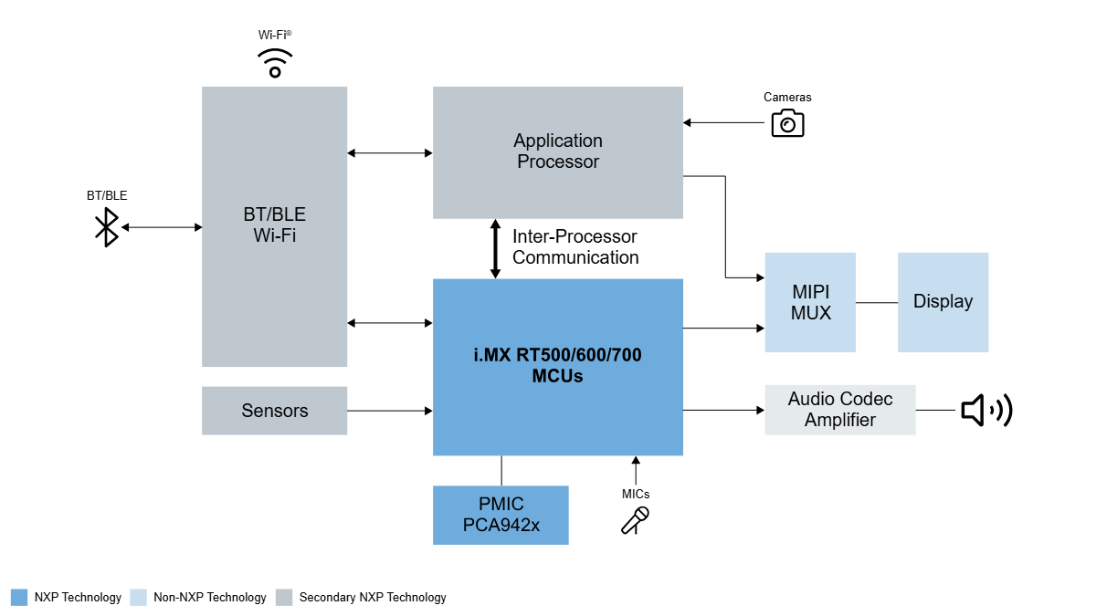
NXP’s Solution: The i.MX RT Family as the Ideal Coprocessor
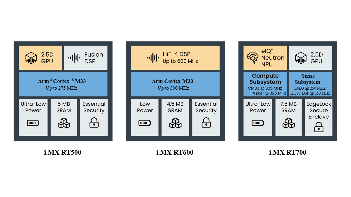
The i.MX RT500, i.MX RT600 and i.MX RT700 has three chips in NXP’s i. MX RT low-power product family. These chips, as coprocessors, are currently widely used in the latest AI eyewear designs for many customers around the world. The i.MX RT500 Fusion F1 DSP can support voice wake-up, music playback, and call functions of smart glasses. The i.MX RT600 is mainly used as an audio coprocessor for smart glasses, supporting most noise reduction, beamforming, and wake-up algorithms. The i.MX RT700 features dual DSP (HiFi4/HiFi1) architecture and supports algorithmic processing of multiple complexities, while enabling greater power savings with the separation of power/clock domains between compute and sense subsystems.
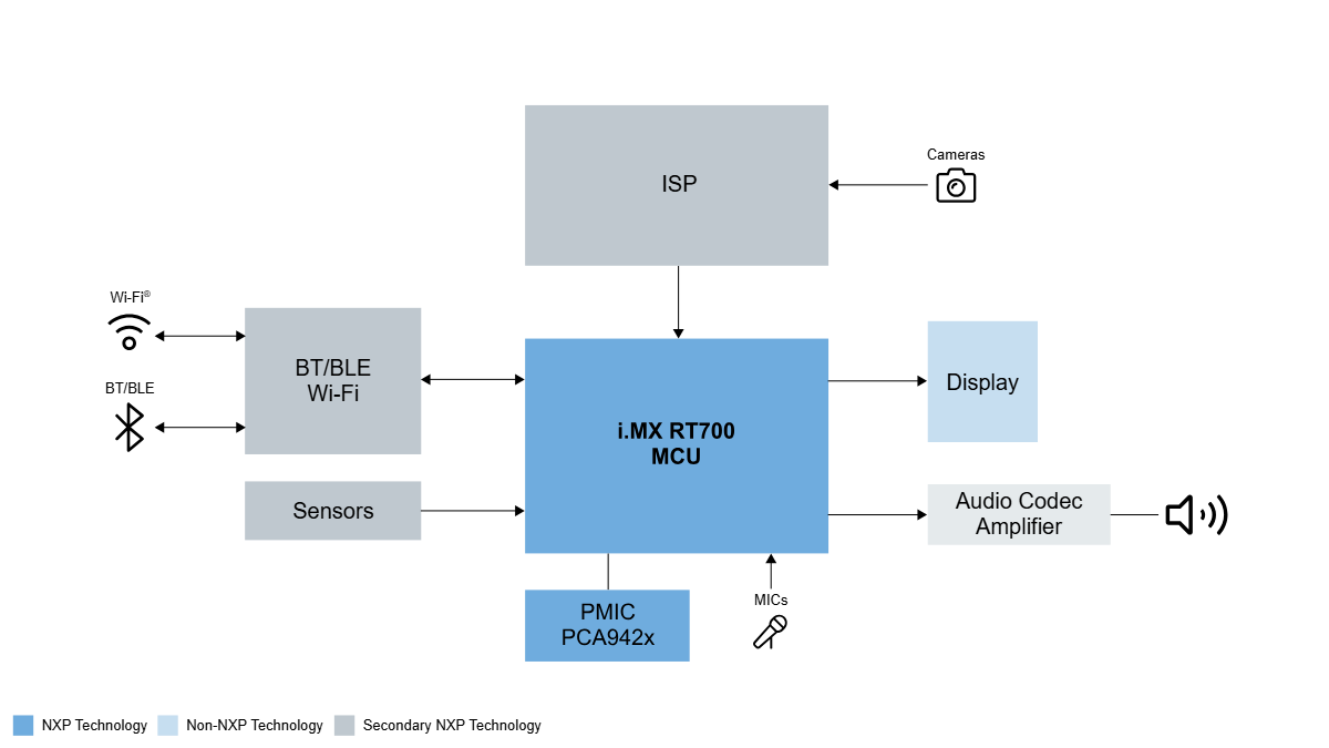
How the i.MX RT700 Maximises Battery Life
As a coprocessor in AI glasses, the i.MX RT700 can flexibly configure power management and clock domains to switch roles based on different application scenarios: it can be used as an AI computing unit for high-performance multimedia data processing, and it can also be used as a voice input sensor hub for data processing in ultra-low power consumption.
AI glasses mainly rely on voice control to achieve user interaction, so voice wake-up is the most commonly used scenario and the key to determining the battery life of AI glasses. In mainstream use cases, the coprocessor remains in active mode at the lowest possible core voltage levels, awaiting the user’s voice commands, quickly switching to speech recognition mode with noise reduction in potentially noisy environments. Based on this user scenario, the i.MX RT700 can be configured to operate in sensor mode; at this time, only a few modules, such as HiFi1 DSP, DMA, MICFIL, SRAM, and power control (PMC), are active. The Digital Audio Interface (MICFIL) allows microphone signal acquisition; DMA is used for microphone signal handling; HiFi1 is used for noise reduction and wake-up algorithm execution, while the compute domain is in a power-down state.
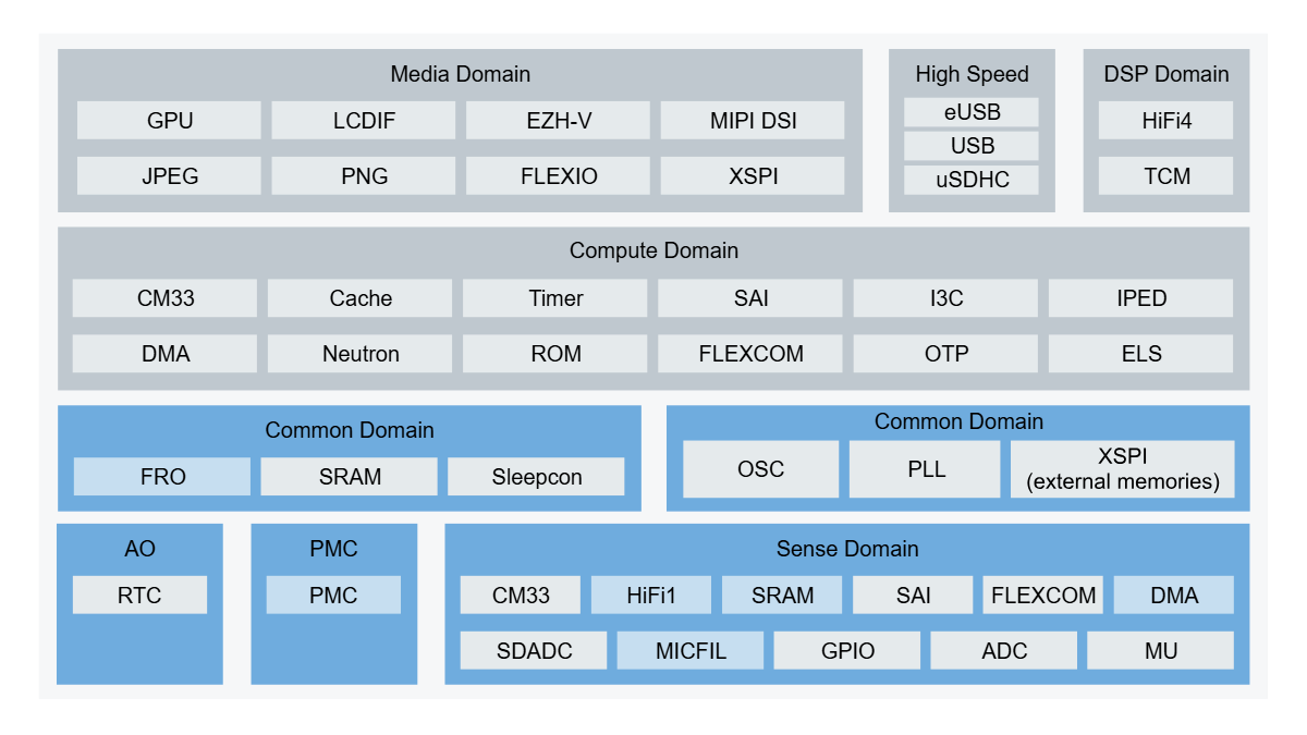
Other low-power technologies included in the RT700, such as distortion-free audio clock source FRO, microphone module FIFO, and hardware voice detection (Hardware VAD), DMA wake-up also ensures that the system power consumption of i.MX RT700 voice wake-up scene can be under 2 mW, maximising power consumption while continuously monitoring.
RT700 also powers MCU-only
For display-related user scenarios, the i.MX RT700 can be configured in “High Performance Mode”, where the Vector Graphics Accelerator (2.5D GPU), Display Controller (LCDIF), and Display Bus (MIPI DSI) are enabled. While enabling high performance, the compute domain also takes advantage of low-power technologies such as MIPI ULPS (Ultra Low Power State), dynamic voltage regulation within the Process Voltage Temperature (PVT) tuning, and other low-power technologies.
With the continuous integration of intelligent hardware and artificial intelligence, choosing the right low-power high-performance chip has become the key to product innovation. With its deep technology accumulation, the i.MX RT series provides a solid foundation for cutting-edge applications such as AI glasses.
The post AI Glasses: Ushering in the Next Generation of Advanced Wearable Technology appeared first on ELE Times.
The semiconductor technology shaping the autonomous driving experience
Courtesy: Texas Instruments
Last summer in Italy, I held my breath as I prepared to drive down a narrow cobblestone road. It was pouring rain with no sign of stopping, and I could hardly see. Still, I pressed the gas pedal, my shoulders tense and my hands gripping the wheel.
This is just one example of a stressful driving experience. Whether it’s enduring a long road trip or crawling through bumper-to-bumper traffic, many people find driving to be nerve-wracking. Though we can spend weeks finding the perfect car, deliberating which seats will feel the most comfortable or which stereo system will sound the richest, it’s hard to enjoy the ride when you are constantly scanning for hazards, adjusting to changing weather conditions, or navigating unknown roadways.
But what if you could appreciate the experience of being in your vehicle while trusting your car to navigate the stressful drives for you?
We’re progressing toward that future, with worldwide investment in autonomous vehicles expected to grow by over US$700 million in 2028. But to understand the vehicle of the future, we must first understand how its architecture is evolving.
How software-defined vehicles (SDVs) are transforming automotive architecture
I can’t discuss the vehicle of the future without starting with the transition to software-defined vehicles (SDVs). Because SDVs have radar, lidar, and camera modules, they are critical to a future where drivers have the latest automated driving features without having to purchase a new vehicle every few years.
For automotive designers, SDVs require separating software development from the hardware, fundamentally changing the way that they build a car. When carmakers consolidate software into fewer electronic control units (ECUs), they can make their vehicle platforms more scalable and streamline over-the-air updates. These ECUs can handle the control of specific autonomous functions in real time, such as automatic braking or self-steering modules.
How integrated sensor fusion enables higher levels of vehicle autonomy
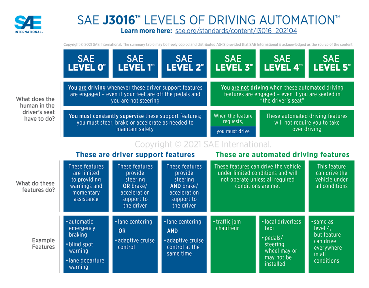
When SDVs centralise software, they’re capable of integrating advanced driver assistance system technologies that enable increased levels of vehicle autonomy. On today’s roads, using the Society of Automotive Engineers’ Levels of Driving Automation, level 1 or 2 (which requires people to drive even when support features are engaged) is the most prevalent. But what about in the future?
I envision that one day, every car will have accurate level 3 or 4 autonomy, characterised by automated driving features that can operate a vehicle under specific conditions. The advances in technology happening now will enable drivers to trust features in future vehicles as much as features like cruise control today. Instead of being fully responsible for stressful driving tasks, we can trust the vehicle’s system to take the lead. And at the heart of this evolution are semiconductors.
To achieve higher levels of vehicle autonomy, the ability to accurately detect and classify objects and respond in real time will require more advanced sensing technologies. The concept of combining data from multiple sensors to capture a comprehensive image of a vehicle’s surroundings is called sensor fusion. For example, if a radar sensor classifies an object as a tree, a second technology, such as lidar or camera, can confirm it in order to communicate to the driver that the tree is 50 feet ahead, enabling swift action.
Why future vehicles need a high-speed, Ethernet-based data backbone
I like to say that tomorrow’s cars are like data centres on wheels, processing multiple large streams of high-speed data seamlessly.
The car’s computer, among other functions, coordinates things such as radar, audio, and data transfer in a high-speed communication network around the vehicle. While legacy communication interfaces for in-vehicle networking, such as Controller Area Network (CAN) and Local Interconnect Network (LIN), remain essential for controlling fundamental vehicle applications such as doors and windows, these interfaces must seamlessly integrate with emerging technologies. In order to accommodate the higher data processing needs of new vehicles, Ethernet will be the prevailing technology. Automotive Ethernet has emerged as a “digital backbone” to efficiently manage applications ranging from audio to standard radar.
As vehicles become capable of higher levels of autonomy, automotive designers will need higher-bandwidth networks for applications including high-resolution video and streaming radar. At TI, our portfolio supports diverse functions with varying requirements, readying us for that network evolution. With technologies like FPD-Link, vehicles can stream uncompressed, high-bandwidth radar, camera, and lidar data to the central compute to respond to events in real-time.
Design engineers must also have a powerful processor in the central computing system that can take data from multiple technologies, such as lidar, camera, and radar sensors, to complete a fast, real-time analysis and provide a 4D data breakdown to better perform object classification.
With expertise in radar, Ethernet, FPD-Link technology and central compute, TI works with automotive designers to help optimise solutions from end to end. Rather than designing devices that only perform one function, we look at how to best optimise our device ecosystem. For example, we design radar devices that easily interface with our Jacinto processors to achieve faster, more accurate decision-making.
What these advancements mean for the future driving experience
In the future, if I encounter the same road and rainy conditions in Italy as I did this summer, I might not drive. Instead, I might trust my car to safely get me to my destination, while I relax in my seat.
The vehicle of the future might not exist yet. But the technologies we’re developing today are making the vehicle of the future – and maybe even the next breakthrough of the future – real.
The post The semiconductor technology shaping the autonomous driving experience appeared first on ELE Times.
The electronics Industry in 2026 and Beyond: A Strategic Crossroads
As we stand on the threshold of 2026, the global electronics industry is undergoing a profound transformation. It is now a linchpin of industrial, strategic, and geopolitical competition, with implications for economies, national security, and everyday life. In a world where electronic systems power everything from personal communication to national infrastructure, the industry’s trajectory through 2026 and beyond will be a trendsetter for economic competitiveness and technological leadership worldwide.
Worldwide, electronic systems and semiconductor markets have regained strong growth momentum following recent supply fluctuations and trade tensions. In major economies, consumer-facing electronics still matter – smart TVs, connected appliances and IoT devices feature prominently in growth forecasts – but industrial and strategic demand is shaping the industry’s future. AI acceleration, 5G/6G networks, edge computing and automated factories are expanding the role of electronics far beyond personal use into the backbone of tomorrow’s digital economy.
For emerging economies like India, 2026 marks a pivotal year. Once predominantly an assembly hub, India’s electronics landscape is evolving quickly toward manufacturing depth and export competitiveness. Under initiatives like Make in India and Production-Linked Incentive schemes, India is targeting an ambitious USD 300 billion in domestic electronics production by 2026.
Despite progress in finished products, the industry’s most strategic component – the semiconductor – remains the ultimate litmus test of technological sovereignty. Demand for advanced logic, memory and power chips continues to skyrocket as AI, data centres, autonomous systems and EVs proliferate. However, high-end semiconductor fabrication is concentrated in a few global hubs, creating political and economic frictions. Expansion efforts are underway; India aims to bring complex chip manufacturing and packaging closer to local markets.
Now the industry’s evolution will hinge on architectural and material innovation as much as volume growth. Emerging manufacturing techniques like 3D-printed electronics, wide-band-gap power devices (such as GaN and SiC), and advanced packaging are reshaping how electronic systems are built and what they can do.
Integration with AI and machine learning at the edge – beyond centralised cloud systems – is transforming everything from consumer devices to industrial controls. AI-powered industrial machines, smart wearables and edge computing systems are now central to innovation narratives that go far beyond smartphones and laptops.
Governments play a deciding role in semiconductor incentives, R&D investment, and skills ecosystem development. India’s push into electronics manufacturing underscores how policy can unlock domestic value addition and attract foreign direct investment.
A young workforce is being credited with driving innovation in design labs and new technology ventures. This demographic shift could help transcend low-value assembly toward high-value engineering and R&D.
By the end of the decade, the core electronics industry will be defined by: reducing reliance on limited geographic hubs for chips and components; hardware designed for AI workloads will proliferate; energy efficiency and green manufacturing will be essential competitive factors, and new alliances and regional clusters will diversify global supply chains.
Let us check a few facts about a comprehensive, forward-looking overview of India’s electronics industry – where it stands now, the key forces shaping its future, and what lies ahead in the coming decade. India’s electronics production rose from Rs. 1.9 lakh crore in 2014–15 to Rs. 11.3 lakh crore in FY 2024–25 – a six-fold jump in a decade. Exports have similarly surged eightfold in that period.
Production Linked Incentive schemes significantly boost manufacturing across mobile phones, IT hardware, and components. The Electronics Components Manufacturing Scheme offers capital subsidies to build domestic production of PCBs and critical parts. The Scheme for Promotion of Manufacturing of Electronic Components and Semiconductors supports capital expenditure for high-value component plants. These policies aim to reduce dependence on imports, attract foreign investors, and expand high-value manufacturing. The global supply-chain shift, e.g., China + 1 strategies, is prompting electronics makers to diversify production to India. States like Uttar Pradesh, Tamil Nadu, Karnataka, and Andhra Pradesh are becoming hubs for manufacturing and exports — bringing infrastructure and investment.
There are certain challenges that India must overcome. It includes Component Import Dependency – despite growth in assembly, 85–90 % of electronics component value is still imported, especially from China, Korea, and Taiwan. Building domestic supply chains for PCBs, semiconductors, connectors, and precision parts remains a major hurdle. Bureaucratic delays in certifications are slowing production schedules and product launches. Production costs in India can be 10–20 % higher than in other Asian hubs, and R&D infrastructure for high-end semiconductors is still limited. India needs deep innovation capacity – not just assembly, but to move up the value chain.
India has set a target for itself for the coming years, such as a target of up to USD 500 billion in electronics manufacturing output by 2030. Achieving this would require scaling capacity, improving infrastructure, and drawing more global players into deeper parts of the supply chain. India needs to broaden Electronics Ecosystem Growth – Automotive electronics, industrial IoT, wearables/AI devices, and telecom equipment to expand domestic and export markets. EMS output is projected to grow rapidly, potentially capturing a larger share of the global EMS market. Semiconductor Ecosystem Development – policies are moving into a “scale-up phase” to build design, assembly, and, over time, manufacturing capabilities – crucial for tech sovereignty and global relevance. Global shifts in supply chain diversification present opportunities for India to attract investments that might otherwise be concentrated in China or Southeast Asia.
Geopolitical-economic dynamics are a significant stumbling block for India’s electronics industry, especially in relation to China and the United States – but it’s also both a challenge and an opportunity.
India’s electronics manufacturing growth has been strongly influenced by global tensions between China and the U.S. After the pandemic and during the U.S.-China trade/tech war, global supply chains began diversifying away from China – a “China +1” effect – and India benefited from this shift as multinational firms looked for alternatives for parts of their production.
Despite India’s assembly growth in mobile phones and other electronics, the industry remains heavily reliant on Chinese imports for key components and machinery. This dependency means that geopolitical friction with China can slow production, raise costs, and create supply bottlenecks for Indian electronics makers.
U.S.-India trade Frictions are also impacting growth. The U.S. imposed a high tariff of up to 50 % on Indian goods, which affects overall trade dynamics that make it harder for Indian electronics producers to scale exports cost-effectively. Hence, India is caught in a complex geopolitical squeeze: China remains essential for many inputs but is a strategic rival, while the U.S. provides market and technology ties but has also used tariffs as leverage.
On the other hand, India’s electronics exports to the U.S. had raced ahead by leveraging trade tensions that kept Chinese goods less competitive. But the recent reduction of U.S.–China tariffs has reduced India’s cost edge by around 10 percentage points, threatening export growth and investment momentum in the sector. India’s industry competitiveness isn’t purely industrial – it’s shaped by geopolitical policy decisions in Washington and Beijing.
Nevertheless, India’s electronics industry is poised for one of the most transformative growth phases in its history. With supportive policy frameworks, rising global demand, and strategic investments in talent and infrastructure, India could evolve from a largely assembly-focused hub to a comprehensive electronics and semiconductor powerhouse over the next decade – if it successfully strengthens its component base, resolves regulatory bottlenecks, and nurtures innovation ecosystems.
Devendra Kumar
Editor
The post The electronics Industry in 2026 and Beyond: A Strategic Crossroads appeared first on ELE Times.
Keysight & Samsung: Industry-First NR-NTN S-Band & Satellite Mobility Success
Keysight Technologies announced a groundbreaking end-to-end live new radio non-terrestrial networks (NR-NTN) connection in band n252, as defined by the Third Generation Partnership Project (3GPP) under Release 19, achieved using Samsung Electronics’ next-generation modem chipset. The demonstration, taking place at CES 2026, includes live satellite-to-satellite (SAT-to-SAT) mobility using commercial-grade modem silicon and cross-vendor interoperability, marking an important milestone for the emerging direct-to-cell satellite market.
The achievement also represents the public validation of n252 in an NTN system, a new band expected to be adopted by next-generation low Earth orbit (LEO) constellations.
Reliable global connectivity is a growing requirement for consumers, vehicles, IoT devices, and critical communications. As operators, device manufacturers, and satellite providers accelerate investment in NTN technologies, this achievement shows decisive progress toward direct-to-cell satellite coverage.
With the addition of n252 alongside earlier NTN demonstrations in n255 and n256, all major NR-NTN FR1 bands have now been validated end-to-end. This consolidation of band coverage is critical for enabling modem vendors, satellite operators, and device manufacturers to evaluate cross-band performance and mobility holistically as they prepare for commercial NTN services.
Keysight’s NTN Network Emulator Solutions recreate realistic multi-orbit LEO conditions, SAT-to-SAT mobility, and end-to-end routing while running live user applications over the NTN link. Together with Samsung’s chipset, the system validates user performance, interoperability, and standards conformance, providing a high-fidelity test environment that reduces risk, accelerates trials, and shortens time-to-market for NR-NTN solutions expected to scale in 2026.
The demonstration integrates Samsung’s next-generation modem chipset with Keysight’s NTN emulation portfolio to deliver real, standards-based NTN connectivity across a complete system. The setup validates end-to-end link performance, mobility between satellites, and multi-vendor interoperability, essential requirements for large-scale NTN deployments.
Peng Cao, Vice President and General Manager of Keysight’s Wireless Test Group, Keysight, said: “Together with Samsung’s System LSI Business, we are demonstrating the live NTN connection in 3GPP band n252 using commercial-grade modem silicon with true SAT-to-SAT mobility. With n252, n255, and n256 now validated across NTN, the ecosystem is clearly accelerating toward bringing direct-to-cell satellite connectivity to mass-market devices. Keysight’s NTN emulation environment enables chipset and device makers a controlled way to prove multi-satellite mobility, interoperability, and user-level performance, helping the industry move from concept to commercialisation.”
The post Keysight & Samsung: Industry-First NR-NTN S-Band & Satellite Mobility Success appeared first on ELE Times.
Quantum Technology 2.0: Road to Transformation
Courtesy: Rhode & Schwarz
After more than 100 years of research, quantum technology is increasingly finding its way into everyday life. Examples include its use in cell phones, computers, medical imaging methods and automotive navigation systems. But that’s just the beginning. Over the next few years, investment will increase significantly, and lots of other applications will take the world by storm. While test & measurement equipment from Rohde & Schwarz and Zurich Instruments is helping develop these applications, the technology group’s encryption solutions are ensuring more secure communications based on quantum principles.
Expectations for quantum technology are greater than in almost any other field. That’s no surprise, given the financial implications associated with the technology. For example, consulting firm McKinsey & Company estimates the global quantum technology market could be worth 97 billion dollars by 2035. According to McKinsey, quantum computing alone could be worth 72 billion dollars, and quantum communications up to 15 billion.
Previous developments clearly show that the projected values are entirely realistic. Many quantum effects have become part of our everyday lives. Modern smartphones, for example, contain several billion transistors, predominantly in flash memory chips. Their function – controlling currents and voltages – is based on the quantum mechanical properties of semiconductors. Even the GPS signals used in navigation systems and the LEDs used in smartphone flashlights are based on findings from quantum research.
To celebrate these achievements, UNESCO declared 2025 the “International Year of Quantum Science and Technology” – exactly 100 years after German physicist Werner Heisenberg developed his quantum mechanics theory based on the research findings of the time. Quantum technology was also in the spotlight with the 2025 Nobel Prize in Physics, which was awarded to quantum researchers John Clarke, Michel Devoret, and John Martinis.
Quantum technology 2.0: what can we expect?Quantum physics in secure communications: Whether personal or professional, beach holiday snapshots or development proposals for new products, our data and data transmission need to be protected. Companies today consistently name cyberattacks and the resulting consequences as the top risk to their business. Developments in quantum computing are revealing the limits of conventional encryption technologies. Innovations in quantum communications are the key to the future, as they enable reliable detection of unauthorised access. This means you can create a genuine high-security channel for sensitive data.
Upgrading supply chains: Global flows of goods reach every corner of the Earth, and everything is now just a click away: a new tablet for home use or giveaways for a company party. But behind the scenes lies a complex logistics network of manufacturers, service providers, suppliers, merchants, shipping companies, courier services, and much more. The slightest backlog at a container port or change in the price of purchased items means alternatives must be found – preferably in real time. But the complexity of this task is also beyond what conventional computers can handle.
Personalised medicine: Everyone is different, and so are our illnesses. Cancer cells, for example, differ from one person to the next and often change over time. These differences and changes are already well documented in analytical terms, which has created huge amounts of data. Big Data is the buzzword. But evaluating this data quickly and effectively, to develop personalised forms of treatment, is impossible for conventional computers.
Fast. Faster. Quantum computing.
Our world is controlled by binary code. Conventional computers process data as sequences of ones and zeros, true or false, off or on. This applies to everything, from simple text processing to virtual reality in the metaverse. But the world we live and work in is becoming increasingly complex. The amount of data we need to process is growing rapidly. In 2024, global digital data traffic had more than quadrupled over the space of just five years to 173.4 zettabytes. By 2029, experts believe this number will reach 527.5 zettabytes, equivalent to 527.5 trillion gigabytes.
Conventional computers face two insurmountable obstacles as a result: time and complexity. The larger the volume of data, the more time you need to process that data sequentially. The more complex the problem, the lower the probability that a binary code, with only two states, will be able to efficiently calculate a solution. Quantum computers have the potential to overcome both obstacles using insights from modern physics.
Hand in hand instead of either-or
Like conventional bits, quantum bits (qubits) form quantum mechanical memory units. In addition to just zeros and ones, they can also assume overlapping, mixed states. This simultaneity represents a fundamental technological paradigm shift. We can now run conventional sequential calculation methods simultaneously, which is why a quantum computer can save so much time.
But above all, the new quantum mechanical approach allows us to process new and much more complex questions. However, it’s not an either-or decision, either conventional processing power or quantum computing. Instead, what matters is integrating existing and quantum systems depending on the task.
Physics versus logic
In the quantum world, a particle can be in two places at the same time. Only when it is observed can you narrow down its location, for example, by measuring it. This unusual property is also why it is extremely unstable. Instead of using individual physical qubits, which can be very error-prone, multiple qubits are grouped into a logical qubit. However, the challenge here is that you need quantum systems with as many as one million logical qubits in order to answer practical questions, like protein folding. A logical qubit can contain up to 100 physical qubits, but the highest processing capacity is currently only 1,225 physical qubits.
Zurich Instruments has been part of the Rohde & Schwarz family since 2021. The T&M market for quantum computing holds enormous potential for both companies. Operating and maintaining quantum computers requires a wide range of specific T&M solutions because RF signals need to be generated and measured with extremely high precision to effectively create and record quantum states. Control systems for quantum computers are part of the company’s portfolio.
Secure. More secure. Quantum communications
Quantum computers have the potential to push the limits of processing efficiency. But this brings challenges, including secure communications – increasingly a priority in view of “Q-Day”, the point at which quantum computers will be able to crack classic encryption.
That is why alternative encryption methods are becoming increasingly important. There are essentially two main approaches. The first is post-quantum cryptography, which involves conventional encryption methods with one key difference: they can survive attacks from quantum computers unscathed. The algorithms used in this approach are based on theoretical assumptions for which no effective attacks are currently known using either quantum or conventional computers.
The other approach relates to quantum key distribution (QKD). The German Federal Office for Information Security (BSI) and the National Institute of Standards and Technology (NIST) are two of the main drivers of innovation in this area. In an increasingly digitalised world, private-sector customers, and government customers in particular, are dependent on trustworthy IT security solutions. Secure communications networks have become a critical infrastructure in advanced information societies.
These innovative solutions are shifting the focus of cryptology. Conventional methods, as well as more recent post-quantum methods, are based on mathematical assumptions, i.e. the idea that certain tasks cannot be calculated with sufficient efficiency. Quantum key distribution, by contrast, is based on physical principles. Rohde & Schwarz Cybersecurity is providing and leveraging its extensive expertise in security solutions, as well as its experience in building and implementing secure devices and systems, in a variety of research projects.
The post Quantum Technology 2.0: Road to Transformation appeared first on ELE Times.
Develop Highly Efficient X-in-1 Integrated Systems for EVs
Courtesy: Renesas
The recent tightening of CO2 emission regulations has accelerated the electrification of automobiles at an unprecedented pace. With the global shift from hybrid vehicles to electric vehicles (EVs), automakers are demanding more efficient, safe, and reliable systems. System integration, known as “X-in-1”, becomes the focus of attention. This innovative concept integrates functions traditionally controlled by separate MCUs, such as inverters, onboard chargers (OBC), DC/DC converters, and battery management systems (BMS), into a single microcontroller (MCU), achieving simultaneous miniaturisation, cost reduction, and efficiency improvement. As electric vehicles evolve, demand grows for X-in-1 configurations that consolidate multiple applications onto a single MCU.
At the core of this X-in-1 approach is Renesas’ RH850/U2B MCUs. This next generation of MCUs delivers the advanced control, safety, and security required by EVs on a single chip. It features a high-performance CPU with up to six cores, operating at up to 400MHz, enabling both real-time control and parallel processing. It also offers comprehensive analogue and timer functions for inverter and power converter applications, enabling efficient control of the entire electrification system on a single chip. Furthermore, the RH850/U2B MCUs offer a wide memory lineup, allowing flexible implementation of the optimal X-in-1 system tailored to specific requirements.
 Figure 1. Comparison of MCU Configuration Before and After X-in-1 Integration
The RH850/U2B MCU demonstrates overwhelming superiority in inverter control, maximising the driving performance of EVs. With dedicated hardware optimised for inverter control, including a resolver-to-digital converter (RDC), an analogue-to-digital converter (ADC), and timers for three-phase motors, the RH850/U2B MCU enables high-speed, high-precision control at the hardware level that software alone cannot achieve. The integrated RDC eliminates the need for external angle detection ICs, contributing to reduced component count and simplified board design. Furthermore, the embedded Renesas proprietary Enhanced Motor Control Unit (EMU) executes complex control calculations in the hardware, significantly reducing CPU load while achieving high-speed, high-precision motor control (EMU is only included in the RH850/U2B6).
 Figure 2. Comparison of External RDC and Internal RDC
The next-generation power devices using silicon carbide (SiC) and gallium nitride (GaN) are increasingly being adopted in OBCs and DC/DC converters. These devices enable high efficiency and fast switching, directly contributing to shorter charging times and improved energy efficiency. On the other hand, the RH850/U2B MCU incorporates a multifunctional timer (generic timer module (GTM)*2 and high-resolution PWM) that is capable of generating high-speed, high-resolution waveforms (minimum resolution of 156.25ps). This facilitates control that leverages the high-speed switching characteristics of SiC and GaN. It also incorporates a 12-bit fast comparator for high-frequency switching control and protection operations.
In addition to speed and energy efficiency, the RH850/U2B MCU also delivers outstanding performance in battery management systems, the heart of EVs. Monitoring and controlling the voltage and temperature of hundreds of cells demands high processing power. The RH850/U2B MCU features a multi-core CPU, allowing surplus resources to be allocated to BMS processing. This enables system miniaturisation and cost reduction without requiring additional MCUs.
As EVs proliferate, the importance of safety and security becomes critical. Compliant with ISO 26262 ASIL D, the RH850/U2B MCU ensures functional safety at the hardware level. It also incorporates security features compliant with EVITA Full, enabling the construction of highly secure systems even in X-in-1 configurations.
The evolution of EVs is moving towards faster, safer, and more efficient use of automobiles. Achieving this requires meeting new demands that conventional MCUs cannot fully address. The RH850/U2B MCU enables users to meet the needs of EVs with high-speed, high-precision inverter control via dedicated hardware; highly efficient switching control in OBCs and DC/DC converters using high-resolution, high-speed timers; multi-core utilisation in battery management systems; and comprehensive safety and security support.
The post Develop Highly Efficient X-in-1 Integrated Systems for EVs appeared first on ELE Times.
Meanwhile, my CPU is on fire.
 | submitted by /u/TallIntroduction8053 [link] [comments] |
КПІ ім. Ігоря Сікорського — лідер серед університетів України у сфері інтелектуальної власності

КПІ ім. Ігоря Сікорського — лідер серед університетів України у сфері інтелектуальної власності за даними Українського національного офісу інтелектуальної власності та інновацій (УКРНОІВІ)
Making a FOSS racing datalogger
 | I'm making a FOSS racing datalogger after I got into kart racing a few years ago and saw how expensive dataloggers were I had to make the GPS laptiming Library, the datalogger itself, designed and printed the case, and recently started on a dataviewer Well all of that took a year to perfect, the laptiming is within 0.002s of the official laptiming, I can do track/course selection, laps, pace, and even split-timing on-device. Now sure, it logs data, but it's not a datalogger without more data. Most other sensors are easy to implement... Engine rpm tho... what a nightmare I'm a software guy, never made hardware before, barely have any idea what I'm doing but i'm making progress. Right now I'm dealing with SD cards being corrupted so I finally gave in and bought a scope to learn more, managed to build a drastically cleaner circuit than I had before and I got some hope. (Yes vibration kills, but this is a new problem with adding the tachometer, and I haven't even gotten to testing that on track yet) (I must do this weird capacitive dance like the "real" ones do, but I also don't have one to take apart so we're gonna just keep winging it baybe) No I don't want to talk about how much money I've spent at this point, I'm making an open source, and cheap, datalogger I probably should have went to school for this but hey, I've gotten this far on nothing but hopes and dreams 20 year SWE brute forcing myself into hardware [link] [comments] |
I am attempting to make a racing datalogger
 | I got into kart racing a few years ago and got pissed off at how expensive dataloggers were($500++), so I went to build one, only to find no ones ever really released many if any public libraries for gps lap timing. So I made one, and then I needed a logger for it, so I made that, then I needed a case, and made that too, and recently cive-coded a data-viewer but that's another rant (20yoe swe) Well all of that took a year to perfect, the laptiming is within 0.002s of the official laptiming, I can do track/course selection, laps, pace, and even split-timing on-device. Now sure, it logs data, but it's not a datalogger without more data. Most other sensors are piss easy to implement... Engine rpm tho... My god what a nightmare I'm a software guy, never made hardware before, barely have any idea what I'm doing but by God I'm making progress. Right now I'm dealing with SD cards being corrupted so I finally gave in and bought a scope to learn more, managed to build a drastically cleaner circuit than I had before and I got some hope. (Yes vibration kills, but this is a new problem with adding the tachometer, and I haven't even gotten to testing that on track yet) (I must do this weird capacitive dance like the commercial ones do, but I also don't have one to take apart so we're gonna just keep winging it baybe) No I don't want to talk about how much money I've spent at this point, I'm making a damned open source, and cheap, datalogger so help me God I've got GitHub links for everything but don't wanna get yelled at dropping links in a first post or something I probably should have went to school for this but hey, I've gotten this far on nothing but hopes and dreams [link] [comments] |
start of my fpga programing journey a 1 bit alu on t41 thinkpad
 | submitted by /u/Green-Pie4963 [link] [comments] |
EEVblog 1729 - AC Basics Tutorial Part 7: AC Ohms Law
Electronic circuit simulation engine for education
 | Hi Reddit, While reading the Charles Petzold's great vulgarization book CODE : The Hidden Language of Computer Hardware and Software I told myself that it would be a cool educational project to animate the book schemas to vulgarize how computers work down to the transistor level. So I created an electronic circuit engine to help discovering how electronics and computers work. You can check the demo here. This is a starting open source project and all comments and feedback are very welcomed ! [link] [comments] |
Weekly discussion, complaint, and rant thread
Open to anything, including discussions, complaints, and rants.
Sub rules do not apply, so don't bother reporting incivility, off-topic, or spam.
Reddit-wide rules do apply.
To see the newest posts, sort the comments by "new" (instead of "best" or "top").
[link] [comments]
Found this AI generated 20V to 12V converter on the internet. Still laughing my ass off.
 | How the fuck would this even work lmao🤣. [link] [comments] |
Когенерація як частина інженерної освіти: у КПІ за участі RSE запускають навчальну програму в межах Energy Resilience Lab

У КПІ ім. Ігоря Сікорського з наступного семестру запроваджується навчальна дисципліна з когенерації, інтегрована в освітню програму підготовки інженерів-енергетиків. Програма розроблена у партнерстві з інженерною компанією RSE за підтримки GIZ та буде реалізована на базі лабораторії автономного та стійкого енергозабезпечення Energy Resilience Lab.
Perceptra secures €1.2m funding from PhotonDelta
Сторінки


![[link]](https://i.redd.it/0ul7j1yostcg1.jpeg)
![[link]](https://i.redd.it/qwwhx9yitncg1.jpeg)
![[link]](https://i.redd.it/u9c65lnwpkcg1.png)
![[link]](https://i.redd.it/sm3zxk03aicg1.png)