


Збирач потоків
With PEN nearing end-of-life, capacitors built on it must change

For decades, polyethylene naphthalate (PEN) held a small but critical place in high-performance capacitors. It was never the volume material that biaxially oriented polypropylene (BOPP) is, since cost and production capacity kept it niche. But capacitor engineers reached for PEN when BOPP ran out of room: when temperatures climbed, when packages had to shrink, or when a higher dielectric constant was the only way to hit the energy target.
Now capacitor-grade PEN is disappearing. Major suppliers are signaling PEN end-of-life, and capacitor manufacturers serving aerospace, defense, power grids, transportation, and industrial power electronics are asking what comes next.
It’s tempting to treat this as a sourcing problem. In other words, find a comparable dielectric, drop it into the existing capacitor, qualify it, and move on. But that instinct is wrong.
The product you build to replace a PEN capacitor should not be a like-for-like copy with a different dielectric inside. It should be a better capacitor, because major applications are pushing every power electronic component beyond legacy use, and capacitors desperately need to keep up.
Component under the most pressure
AI compute, data center buildout, and electrified transport have driven the most disruptive shift in power demand in generations. Forecasts are rewritten quarterly, interconnection queues are stacking up, and hyperscalers are standing up their own power generation to avoid the wait.
These trends converge on a single component. Capacitors are being asked to handle higher voltages, cycle faster, and survive more thermal stress for decades without drifting out of spec. When program teams walk through where a design holds up or starts to compromise, the conversation lands on the capacitor, its energy density, its footprint and mass, its thermal behavior, and how long it survives the duty cycle.
That conversation is happening earlier in the design cycle than it used to. The capacitor manufacturers responding to these demands earliest are the ones getting designed in.
What PEN capacitor actually did
PEN is at the end-of-life stage, and the capacitors that depend on it can’t just swap in a substitute film and move on. It did two different jobs, and they belong to two different capacitors.
In aerospace pulse power, hardened defense systems, and directed-energy applications, PEN was a high-voltage, energy-dense enabler for rapid discharge. It let designers pack more energy into a smaller capacitor at a given voltage rating.
In EV power electronics, grid subsystems, and rail traction, PEN was chosen not for peak energy density, but for its ability to sustain intense duty cycles and thermal stress, often with a DC bias. A capacitor that functions without derating under all use-scenarios is invaluable to final product design.
Treating those as one problem is what makes PEN replacement feel impossible. It attempts to solve two separate capacitor-design problems, energy density under pulse and thermal stability under load, which should lead to separate design answers.
HDC: Rebuilding the energy-dense capacitor
The first job, exemplified by uses in aerospace, pulse power, hardened defense systems, and fusion, gets picked up by a different class of material entirely. Where PEN was used to shrink a capacitor and push its energy density, the successor is a high dielectric constant (HDC) material, which changes what the capacitor can do, not just what is wound inside it.
Film developers have begun introducing nanolayered metamaterial dielectrics, built from hundreds to thousands of alternating polymer layers, with dielectric constants in the 3.7 to 4.7 range, well above BOPP and many PEN grades, and breakdown strengths of 790 to 820 V/µm. In a finished part, that can mean up to 4× the energy storage in as little as half the footprint of a conventional film capacitor, with improved thermal stability and longer operational life. For a pulse module, a Marx bank, or a grid capacitor competing for volume and mass, is a smaller, lighter, more robust component, not just a spec-sheet footnote.
The trade-off is real and worth stating plainly to a design audience: HDC carries a higher dissipation factor than the lowest-loss dielectrics, so more energy shows up as heat. That constrains how fast and how often the capacitor can be cycled, which is why HDC belongs in energy-density and pulse-duty capacitors—defense pulse modules, mass-constrained aerospace systems, fusion driver banks, and intermittent-duty transportation electronics—rather than continuous switching.
LDF: A lower loss and faster switching capacitor
For the other PEN job—continuous cycling at high repetition rate over decades—the answer is a low dissipation factor (LDF) dielectric, which trades some energy density for very low loss and long thermal endurance in grid inverters, FACTS devices, and industrial drives. This lower dissipation factor means there is less self-heating, greater efficiency of energy transfer, and less stress on components, leading to more reliable and longer lifetimes.
PEN also functions at environmental temperatures above traditional BOPP but below far more expensive alternatives. Due to nanolayering, LDF can incorporate stabilizing layers, which ensure enhanced functionality rivaling PEN, while reducing thermal expansion and device derating. This results in finished capacitors that can be used in hotter or high energy environments without massively increasing component cost.
What capacitor manufacturers should do
PEN’s disappearance marks an inflection point. The capacitor architecture chosen now gets locked in for the life of the platform—30 years or more on the grid and in aerospace. Four moves separate the winners.
- Stop hunting for a one-to-one PEN part
There is no universal replacement capacitor. Segment the installed PEN base by what each capacitor was actually doing—energy density and volume route to HDC, lifetime and efficiency route to LDF—and qualify against that. The segmentation work up-front is what accelerates qualification.
- Design the capacitor for the duty cycle, not the datasheet
AI data centers, EV powertrains, fusion supplies, and grid assets load capacitors differently. A manufacturer who can build to more than one duty cycle expands its addressable market; one who can serve only a single profile gets squeezed.
- Treat heat as a capacitor-and-system problem
HDC trades efficiency for energy density, and that only works if the surrounding power electronics remove the heat. Pair capacitor selection with explicit thermal models and validated test data, and qualifications go faster with fewer field failures.
- Make provenance part of the product
More than 70% of conventional capacitor film originates in China. Buyers hardening the grid, defense platforms, and AI infrastructure are increasingly unwilling to carry that concentration risk. A documented U.S. or allied-nation supply chain is a procurement advantage, and it drops into standard metallizing and winding lines, so qualifying it does not require retooling.
First to qualify, first to win
Those four moves take time to execute, and time is the one input nobody can manufacture more of. Capacitor qualification takes 12 to 24 months. The clock is already running. The manufacturers who commit now to the right capacitor, not the cheapest lookalike, get designed into a decade of rising power demand. Those who requalify a copy of the PEN part will spend that decade watching competitors take the design wins.
Alec Laws is senior product manager for dielectric films at Peak Nano.
Related Content
- Trends in capacitors
- Capacitor matchmaker
- Getting Familiar with Capacitors
- Selecting and Applying Film Capacitors
- Film capacitors: Characteristics and uses in power applications
The post With PEN nearing end-of-life, capacitors built on it must change appeared first on EDN.
DOOM on ESP32-P4: AI plays like a human
DOOM runs on an ESP32-P4 embedded board, and an artificial intelligence plays it by watching the screen, just as a person would. Andrea Ricci’s project uses the SCINTIX P4 board, with a 7-inch MIPI-DSI display and an ESP32-C6 wireless coprocessor. The Claude Sonnet language model controls the game through an MCP interface, without ever accessing the engine’s internal state. The AI only sees what a human player sees: a fan of 51 depth rays, enemies in line of sight, and an ASCII map of already-discovered walls.
The result is an AI gaming experience much closer to a human one. The model doesn’t know the position of demons behind walls, doesn’t know what’s in the next room. It has to explore, remember, and make mistakes. This unusual approach to AI is the heart of the project, and all the source code is in Andrea Ricci’s repository.
Rendering and scaling with the PPADOOM runs entirely on the board, with software rendering at 320×200. The ESP32-P4’s Pixel Processing Accelerator (PPA) does hardware scaling up to 1024×600, the display’s resolution. Scaling time per frame drops from about 24.5 ms with the CPU to about 9 ms with the PPA. DOOM’s software renderer takes about 25 ms per frame, and the game tick runs at 35 Hz (TICRATE). The game maintains about 30 FPS.
The board has 32 MB of PSRAM and 32 MB of flash, with a SPIFFS storage partition of about 12 MB. The 7-inch display is connected via MIPI-DSI, driven by the ST7701S controller. Sound effects audio goes through the ES8311 codec over I2S, with clock derived from SCLK and amplifier disabled via the PI4IOE5V6408 I/O expander.
 The hardware platform
The game is exposed through a ‘lockstep’ WebSocket server. The model sends an action, the game advances a few ticks and returns a structured JSON observation. Then it stops and waits for the next action. An MCP server (tools/doom_mcp_server.py) wraps the WebSocket and registers the game as tools for MCP-compatible clients like Claude Code.
The available tools are: observe, move, shoot, open, select weapon, and map. The observation given to the model is limited to what a player sees: the 51 depth rays, enemies in line of sight (never through walls), the ASCII map, and hints about doors and blocks. Audio is played through the ES8311 codec, with I2C address 0x18, and the I/O expander has address 0x43.
Input and Wi-Fi configurationThe board supports USB input, both keyboard and gamepad. On first power-up, it configures via Wi-Fi with a captive portal. The software uses ESP-IDF v5.5.x, doomgeneric, esp_hosted, and the PPA APIs. The ESP32-C6 coprocessor handles wireless connectivity, while the ESP32-P4 does everything else.
For those who want to get closer to this world, a development board like the ESP32 board with Wi-Fi and Bluetooth can be a first step to experiment with embedded projects. Also, those starting from scratch can use the ESP32-C6-Zero kit to learn the basics of wireless connectivity, before tackling a complex system like this one.
Source: https://github.com/relocsrl/scintix-p4-playing-doom
The post DOOM on ESP32-P4: AI plays like a human appeared first on Open Electronics.
8 to 48 volt PWM relay/solenoid driver finds fault, pinches power

This versatile Design Idea survives and reports open- and short-circuits, not to mention multiplying efficiencies.
Generally accepted tech folklore says that after you drive relays and solenoids into full actuation, only half as much coil voltage and current—and therefore only a fourth as much power—is needed to hold them there. Consequently, driver designs that continuously apply full voltage burn four times the power and heat the coil four times hotter than the job really requires.
Wow the engineering world with your unique design: Design Ideas Submission Guide
Figure 1’s driver circuit employs pulse width modulation (PWM) to dramatically diminish post-pull-in power waste. As an extra added bonus, it also survives and reports open- and short-circuit faults on the GPI status bit.

Figure 1 In this circuit, driver transistor Q2’s PWM duty cycle varies from 100% at actuation to a power saving 50% sustain. It can accommodate load currents up to half an amp. R5 protects current limiter Q3’s base-emitter junction from destruction by over-current events. And Q1 detects coil opens and shorts.
Here’s how it works.
The PWM signal on the general-purpose output (GPO) bit sets Q2’s conduction duty cycle from 0% to 100% to ~50%, from off to full voltage pull-in to quarter-power sustain. Q3 protects Q1 from over-current resulting from shorted coil faults. And Q1 utilizes relay/solenoid coil L1’s inductive “kickback” to detect correct driver operation and report it as a logic “1” on the general purpose input (GPI) pin…or, if kickback is absent (meaning the coil is open or shorted), its logical opposite, “0”.
Figure 2 not-to-scale sketches the driver timing.

Figure 2 In this timing diagram, T1 = timeout to first fault check = L1/R timeconstant = ~500us. T2 = ~100% PWM duty cycle to power initial actuation = ~10ms. T3 = ~50% sustain duty cycle for as long as application requires. And T4 = PWM sustain cycle = ~100us = 10kHz.
In summary, Figure 1’s circuit neither squanders power nor requires changing component values to accommodate different supply voltages. And it’s simple. Along with, dare I say, beautiful? I guess I just did!
Stephen Woodward‘s relationship with EDN’s DI column goes back quite a long way. Over 200 submissions have been accepted since his first contribution back in 1974. They have included best Design Idea of the year in 1974 and 2001.
Related Content
- Booster circuit enables reliable solenoid operation
- The overcurrent limiting transistor fails before anything else!
- Three discretes suffice to interface PWM to switching regulators
- Automotive low side output switch architecture suitable for 8 to 48 volt buses and beyond
The post 8 to 48 volt PWM relay/solenoid driver finds fault, pinches power appeared first on EDN.
The 5G Radio Fog: Why Traditional Spectrum Analysers Miss Modern RF Interference

By Meryem Berrada, Product Marketing Engineer, Keysight Technologies
Modern 5G network testing depends on real-time spectrum analysis to detect transient RF interference that traditional swept spectrum analysers often miss. As RF environments become denser with 5G, IoT, radar systems, and autonomous infrastructure, engineers increasingly rely on handheld spectrum analysers and spectrum management software to identify, localise, and mitigate interference in real time.
The wireless world is not just getting faster. It is getting denser. As global infrastructure shifts toward 5G, massive IoT, and autonomous systems, the RF spectrum is becoming an increasingly crowded and contested space. What once appeared as occasional interference is now evolving into something far more consequential: an invisible gridlock forming across the airwaves. This shift fundamentally changes the nature of the problem.
Interference is no longer a minor inconvenience behind a dropped call. It is a systemic risk capable of disrupting critical operations. Maintaining network integrity now requires more than simply detecting signals. It demands real-time, intelligent awareness of spectrum behaviour as it unfolds. Several key shifts show just how much the RF landscape has changed.
Why Is RF Interference Detection Critical for Safe 5G Network Testing?The transition to 5G does not just improve performance. It raises the stakes. Networks are moving from human-driven communication toward machine-to-machine ecosystems, where reliability is directly tied to physical outcomes. In this environment, RF interference detection affects far more than connectivity. It can directly impact systems such as autonomous vehicle navigation, public safety communications, and radar and defence infrastructure.
In these contexts, failure is not measured in inconvenience. It is measured in consequence. A momentary disruption can cascade into a critical system failure, leaving little to no margin for error. Interference is no longer something networks can simply tolerate. It is something they must actively anticipate and mitigate during 5G network testing and deployment.
Why Do Traditional Spectrum Analysers Miss Modern RF Interference?Conventional swept-tuned spectrum analysers were designed for a very different RF environment, one where signals were relatively stable, predictable, and easier to isolate. Today’s signals behave differently. They are often transient, lasting only milliseconds. They can be intermittent in nature and increasingly dense, overlapping within the same spectral space. Traditional swept spectrum analysers measure frequencies sequentially.
That sweep-based approach can provide useful snapshots of RF activity, but it can also miss short-duration events that occur between sweeps. Real-time spectrum analysis changes that perspective. Instead of sampling the spectrum in slices, it continuously captures and processes RF activity across a defined bandwidth without gaps in observation. This makes it better suited to detecting transient, burst, and intermittent signals that are common in modern 5G and dense RF environments.
With modern tools, engineers can visualise RF behaviour using spectrograms and waterfall displays. These views reveal short-duration transients, overlapping emitters, and time-varying interference patterns that would otherwise remain invisible. Capturing this kind of wideband, time-sensitive activity is no longer a specialised capability. It is becoming a baseline requirement for modern RF interference detection.
Traditional vs. Real-Time Spectrum Analysis: Key Differences for 5G and RF Interference DetectionUnderstanding the difference between traditional and real-time spectrum analysis is critical for engineers performing RF interference detection and 5G network testing in modern environments.
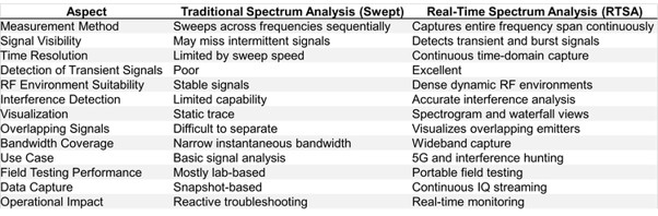 Table 1. Comparison of traditional swept spectrum analysis and real-time spectrum analysis for modern RF interference detection and 5G network testing.
How Are Real-Time Spectrum Analysis Workflows Changing Field Testing?
Table 1. Comparison of traditional swept spectrum analysis and real-time spectrum analysis for modern RF interference detection and 5G network testing.
How Are Real-Time Spectrum Analysis Workflows Changing Field Testing?
The traditional model of RF troubleshooting, dispatching teams to investigate issues on-site, is rapidly becoming unsustainable. Historically, diagnosing problems in the “last mile” required manual drive testing, consuming significant time, labour, and operational resources. That model is now shifting toward centralised, software-driven workflows.
By combining ruggedised handheld spectrum analysers with centralised analysis platforms, engineers can remotely control distributed test assets, monitor multiple sites simultaneously, and stream live measurement data back to centralised teams. This creates a fundamentally different workflow: capture, stream, analyse, and act. Engineers no longer need to be physically present at every field location. Instead, units can remain deployed at the edge while analysis happens centrally, powered by high-fidelity, wideband IQ data delivered in real time.
How Does Real-Time RF Interference Detection Use TDoA Localisation?The classic “fox hunt,” tracking interference sources with directional antennas, was built for a slower and simpler RF environment. In today’s dense 5G deployments, where interference sources can appear and disappear in milliseconds, manual methods struggle to keep pace. The modern approach shifts the problem from physical pursuit to mathematical computation. Time Difference of Arrival, or TDoA, techniques use multiple GPS-synchronised receivers to measure the precise arrival time of a signal across different locations.
Because RF propagation speed is constant, software can calculate the emitter’s position based on the difference in arrival times. This approach reduces reliance on slow, manual triangulation and enables rapid, wide-area localisation that scales with the complexity of modern networks. RF interference detection is no longer only a field exercise. It is increasingly a data-driven problem solved through coordinated measurement and computation.
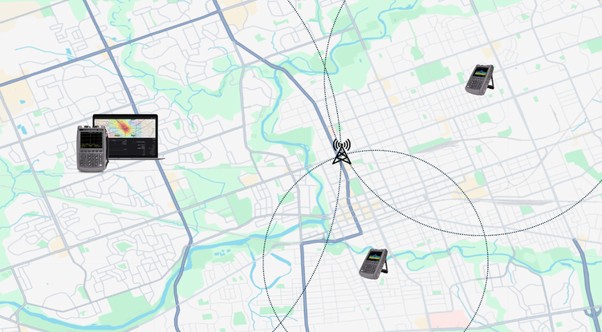 Figure 2. Distributed field measurements combined with TDoA processing enable rapid, wide-area localisation of interference sources
How Are Handheld Spectrum Analysers Closing the Gap Between Field and Lab Testing?
Figure 2. Distributed field measurements combined with TDoA processing enable rapid, wide-area localisation of interference sources
How Are Handheld Spectrum Analysers Closing the Gap Between Field and Lab Testing?
For years, RF engineers had to choose between portability and performance. Handheld spectrum analysers offered convenience in the field but often lacked the depth required for advanced analysis. Benchtop instruments delivered precision, but at the cost of mobility. That trade-off is now changing.
Modern handheld analysers can enable wideband real-time IQ streaming, representing a significant leap from previous limitations and changing what can be achieved outside the lab. This capability is especially important for 5G New Radio, where channel bandwidths can reach up to 100 MHz in sub-6 GHz bands. Without wideband capture, engineers may be forced to stitch together narrower measurements, losing critical time-domain behaviour in the process. With wideband streaming, entire 5G channels can be captured in a single acquisition, preserving signal behaviour and enabling integration into centralised analysis workflows. In practical terms, the boundary between field and lab is becoming less rigid. More advanced analysis can now be brought closer to where the RF problem actually occurs.
Why Real-Time Spectrum Analysis Is Becoming Essential for 5G Network TestingSpectrum management is undergoing a fundamental transformation. Detecting signals is no longer sufficient. Engineers must now be able to capture transient, wideband RF activity in real time, stream and classify that data within centralised systems, precisely locate interference sources, and act before disruptions escalate into failures.
The wideband reality is already here. With 5G NR channel bandwidths reaching up to 100 MHz in sub-6 GHz bands, real-time wideband capture is not just a forward-looking requirement. It is an immediate need for modern 5G network testing. The question is no longer whether interference will occur. The question is whether your tools can see it in time.
The post The 5G Radio Fog: Why Traditional Spectrum Analysers Miss Modern RF Interference appeared first on ELE Times.
PikeOS adds support for the rugged Kontron VX3060 board
SYSGO, a leading European supplier of real-time operating systems and hypervisors for safety and security-critical embedded applications, and Kontron, a global provider of IoT/Embedded Computing Technology (ECT), have announced the availability of a validated Board Support Package (BSP) for the rugged VPX Kontron VX3060 board, based on 11th generation Intel® Core processors. The new BSP extends the long-standing collaboration between the two companies, providing a reliable European hardware and software foundation for safety, security and mission-critical embedded applications.
Designed for demanding markets such as defence, transportation and industrial automation, the combined solution helps system developers speed up platform integration, taking advantage of PikeOS’s advanced virtualization and separation capabilities on a proven VPX computing platform.
 The Kontron VX3060 board with an 11th generation Intel Core processor, supported by the PikeOS BSP.
Developers can immediately deploy PikeOS on the Kontron VX3060 or on Kontron systems such as HARAKAN-F2 that integrate the VX3060, using a fully supported BSP, significantly reducing platform integration effort and accelerating the development of safe and mixed-criticality embedded systems. The BSP supports the board’s key features, including Ethernet, UART, thermal sensors, voltage monitoring sensors and mass storage interfaces. Additional platform security capabilities such as Trusted Platform Module (TPM) integration and Secure Boot are available on customer request to meet cyber resilience challenges and platform integrity requirements. The availability of the BSP accelerates time-to-market, shortens software bring-up times and gives developers a robust starting point for building certified and security-critical systems.
Mixed-criticality support and secure virtualizationThe Kontron VX3060 and the HARAKAN-F systems based on it are designed to operate in harsh operating environments and are suitable for transportation, defence, industrial automation and other applications that require rugged computing platforms. With PikeOS support, customers can immediately take advantage of PikeOS’s advanced partitioning and virtualization capabilities on the platform. PikeOS can operate as a secure hypervisor and as a combined hypervisor and real-time operating system, all in a single product. This flexibility allows developers to consolidate multiple applications with different criticality levels on a single hardware platform while maintaining strict separation between workloads. Critical real-time functions can run alongside Linux, middleware or application environments, enabling efficient mixed-criticality architectures that reduce system complexity, size, weight, power consumption and lifecycle costs.
Strengthening a European technology ecosystemAs demand for reliable European technologies continues to grow in critical sectors, the collaboration between SYSGO and Kontron offers customers an integrated technology stack, combining proven embedded hardware, real-time virtualization and advanced cybersecurity capabilities.
“Our customers increasingly expect embedded computing platforms to be backed by mature software ecosystems,” said Sébastien Vitre, Product Manager at Kontron. “By extending PikeOS support to the VX3060, we give developers a validated hardware and software platform that reduces integration effort and enables faster deployment of secure and mixed-criticality applications.”
“The availability of PikeOS on the Kontron VX3060 demonstrates the continued success of our cooperation with Kontron,” said Carsten Beck, Partner Management at SYSGO. “Together we provide customers with a European technology stack that combines rugged hardware, advanced virtualization, real-time capabilities and the security features needed for next-generation embedded systems.”
The BSP is available immediately and includes support for the main hardware interfaces needed for system boot and application development. Additional security features, including TPM-based trusted computing and Secure Boot, can be integrated according to customer requirements.
The post PikeOS adds support for the rugged Kontron VX3060 board appeared first on Open Electronics.
NDA LAB KPI на Радіотехнічному факультеті

✔️ У КПІ ім. Ігоря Сікорського запрацювала NDA LAB KPI, лабораторія, яку створили спільно з рекрутинговою агенцією NDA Recruitment. Лабораторію відкрили на Радіотехнічному факультеті КПІ, щоб студенти працювали із сучасним обладнанням, перевіряли власні ідеї на практиці, проводили дослідження, створювали й тестували технічні рішення у сфері радіосистем, електроніки та інших технологій.
Paper MOD Player: The Amiga Never Dies
RobDevBuilds has built a MOD player that reads music data printed on paper. The project uses two cameras and stepper motors for optical reading. The goal is to preserve the Amiga’s legacy on a paper medium that could last longer than optical M-Disk discs. The MOD player is not a simple experiment: it is a complete system that plays MOD files by reading paper.
The paper disc and optical readingThe paper disc contains the MOD file’s patterns printed line by line, like in a tracker program. Each voice or instrument has columns of hexadecimal numbers. The back of the disc contains the audio samples and other necessary information, such as metadata and pattern sequence, encoded in a series of barcodes similar to QR codes.
The player uses two cameras, one for each side of the disc. Stepper motors move the cameras like a linear-tracking turntable. The front is read via OCR of the modified Amiga ‘Topaz’ font. The back contains the first 1084 bytes of the MOD file in an inspired QR format created by RobDevBuilds.
The project is documented on the Hackaday.io project page, where RobDevBuilds describes the building process and technical choices. Those who want to dig deeper can check the Hackaday.io project page to see the details of how it works.
Current limits and prospectsThe player currently cannot skip between patterns on the disc as quickly as some MOD files require. This is a known limitation of the project, which RobDevBuilds is addressing. Optical reading of paper is nonetheless a step forward for music file preservation.
The project proposes a method to preserve Amiga MOD files on paper, a medium that could last longer than optical M-Disk discs. Paper is durable and requires no electronics to be stored. Moreover, the printed format is readable even without the player, with OCR or by eye.
To recreate the project you need few components: two cameras, stepper motors, a control system, and a printed paper disc. The most delicate part is printing the patterns and QR codes, which must be precise for optical reading. The rest is mechanics and software, as in many maker projects.
- Two cameras to read the front and back of the disc
- Stepper motors for linear movement of the cameras
- OCR of the Amiga ‘Topaz’ font for the front
- Inspired QR format for the back with the first 1084 bytes of the MOD file
- Paper disc with patterns printed line by line
The paper MOD player is a project that combines music, retrocomputing, and printing. It is not a simple toy: it is a system that could ensure the survival of MOD files for decades, without needing specific hardware to read them. Paper is a medium that does not fear technological obsolescence.
Source: https://hackaday.io/contests
The post Paper MOD Player: The Amiga Never Dies appeared first on Open Electronics.
STMicroelectronics Introduces 1.1 MP Automotive Image Sensor for Affordable In-Cabin Sensing
STMicroelectronics, a global semiconductor leader serving customers across the spectrum of electronics applications, today introduced ST SafeSense VD56GA, a 1.1 MP automotive image sensor for infrared in-cabin sensing. The sensor enables OEMs and Tier 1 suppliers to scale driver and occupant monitoring across vehicle lines while balancing performance, integration, and cost.
As driver and occupant monitoring expands across a broader range of vehicle platforms, automakers and suppliers are looking for imaging solutions that can deliver strong in-cabin performance without adding unnecessary system cost or design complexity. The VD56GA image sensor addresses this need with a compact sensor architecture, high infrared sensitivity, and embedded image-processing capabilities. This combination is designed to provide the image quality required for driver and occupant monitoring while maintaining the size and cost advantages of a compact sensor format. In many in-cabin applications, the VD56GA can help customers meet performance targets without requiring a larger and more expensive sensor.
“In-cabin sensing is moving beyond premium platforms, and carmakers need cost-effective solutions they can deploy broadly,” said Alexandre Balmefrezol, Executive Vice President and General Manager of the Imaging Sub-Group at STMicroelectronics. “With VD56GA, we focused on the system-level tradeoffs that matter most: image quality in infrared conditions, compact integration, and a cost structure that supports high-volume programs. Equally important, the sensor benefits from ST’s Integrated Device Manufacturer model, with front-end manufacturing in Crolles, France, giving customers greater supply-chain resilience, quality control, and long-term support for automotive programs.”
“As driver and occupant monitoring systems move into a broader range of vehicle platforms, OEMs are increasingly focused on solutions that can be deployed at scale, with volumes set to exceed 70 million units by 2031. Success in this market depends not only on imaging performance, but also on reducing system cost, simplifying integration, and enabling adoption across high-volume vehicle programs,” (*) underlined Anas Chalak, Market & Technology Analyst, Imaging at Yole Group.
Helping carmakers scale driver and occupant monitoringVD56GA is designed to help reduce the cost of the complete camera module. Its imaging performance enables the use of lower-cost optics, simplified infrared illumination, less demanding optical filtering, and no external image-processing. For OEMs and Tier 1s, that can translate into a more cost-effective path to deploying driver and occupant monitoring across a broader range of vehicle programs.
The sensor leverages a new backside-illuminated pixel architecture, called ST DeepNIR, optimized for infrared imaging. With 35% higher modulation transfer function (MTF) sharpness and nearly 60% higher quantum efficiency than the previous generation, VD56GA is currently the only sensor in its class to achieve this level of combined optical resolution and infrared sensitivity, helping in challenging conditions like under display camera.
By extracting more performance from a compact 1.1 MP architecture, VD56GA helps automotive designers achieve the image quality required for advanced sensing functions, while benefiting from the integration and cost advantages of a compact sensor architecture.
Compact integration with embedded image processingDesigned for modern automotive camera modules, VD56GA is housed in a compact 3.7 mm x 3.2 mm CSP package, making it suitable for space-constrained installations and next-generation in-cabin camera designs.
The device also integrates a range of embedded image-processing functions, including mirror, crop, dark calibration, auto exposure, and piecewise-linear processing. These features remove the need for external image-processing resources, simplify camera design and speed development.
Support for both RAW and YUV output formats give OEMs and Tier 1 suppliers flexibility across different electronic architectures and software environments, making it easier to adapt the device to a broad range of implementation strategies.
Building on ST’s automotive imaging leadershipVD56GA builds on ST’s established presence in automotive imaging and in-cabin sensing. Earlier this year, ST announced shipment of its 10 millionth automotive of SafeSense by ST image sensors, reflecting broad adoption across key automotive regions, including Europe, Asia, and the United States.
Customers benefit from ST’s vertically integrated manufacturing model and secure supply chain, with front-end manufacturing of VD56GA takes place at ST’s facility in Crolles, France and packaging in Asia; reinforcing the company’s focus on industrial resilience, product quality, and supply continuity for automotive customers worldwide.
The post STMicroelectronics Introduces 1.1 MP Automotive Image Sensor for Affordable In-Cabin Sensing appeared first on ELE Times.
Emerson Expands Bengaluru Test and Measurement R&D Hub by 50% for AI-Driven Engineering
Emerson on 22nd of September, 2026, announced a 50% expansion of its test and measurement research and development (R&D) centre in Bengaluru. The expansion strengthens the facility’s capacity to develop AI-enabled engineering, test software and validation technologies, helping customers address increasing product and validation complexity through more intelligent and software-defined testing approaches.
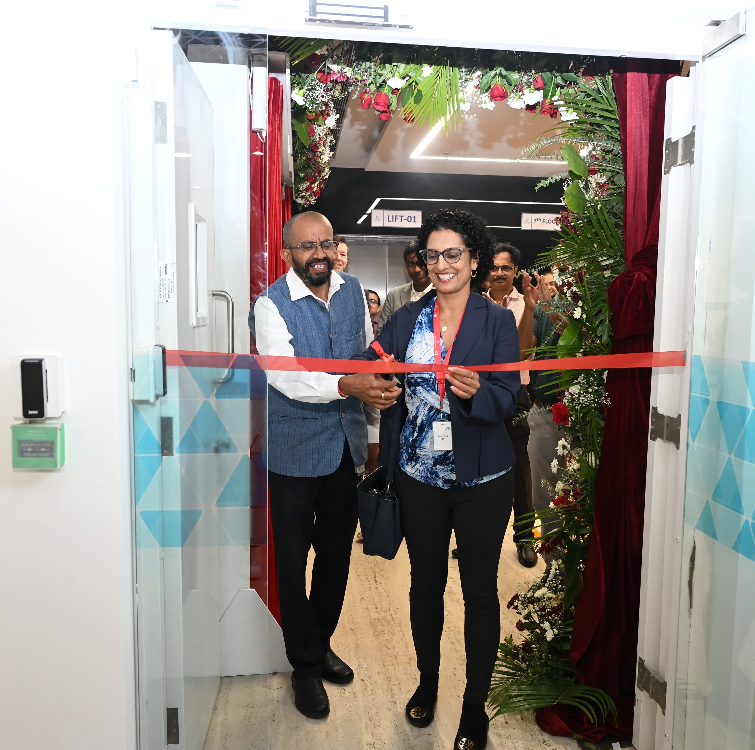
The site also serves as Emerson’s NI Software Center of Excellence and is the company’s second-largest test and measurement R&D centre globally. Engineering teams in Bengaluru develop and support key test software platforms, AI-enabled capabilities, systems engineering technologies and RF test software for global customers across sectors including semiconductors, aerospace and defence, transportation, life sciences, industrial manufacturing, and research and academia. The expansion further advances the site’s transformation from a global capability centre into a global test and measurement innovation centre with global product responsibility.
“Bangalore plays an increasingly strategic role in Emerson’s global test innovation network,” said Ritu Favre, president of Emerson’s Test & Measurement business. “The site combines deep expertise in test software and AI-enabled engineering and validation technologies with close connections to rapidly evolving industries. This investment helps customers manage growing product complexity, streamline validation and bring new innovations to market faster.”

As test systems become increasingly software-driven and AI-enabled, engineers must validate more complex products within shorter development cycles. The expanded Bangalore hub will provide additional capacity to advance automated validation workflows, AI-enabled test engineering and integrated test and measurement platforms for customers worldwide.
India’s continued growth in semiconductors, electric mobility, aerospace and defense is also increasing demand for sophisticated testing and validation. Market development associated with initiatives such as the India Semiconductor Mission and the National Electric Mobility Mission Plan creates opportunities for companies developing, manufacturing and validating new technologies. Emerson is responding to these evolving market needs by expanding its test and measurement R&D capabilities and strengthening its connection to customers and engineering talent in India.
Emerson operates two test and measurement locations in Bangalore: the R&D center and a second site providing application engineering, calibration, sales and customer support. Together, the locations connect global technology development with local market expertise.
The post Emerson Expands Bengaluru Test and Measurement R&D Hub by 50% for AI-Driven Engineering appeared first on ELE Times.
Total beginner, here's my first real project!
 | Before anyone starts cursing me out for how it is made please know that I am extremely new at electronics and this is just to share something I enjoyed making, but also a cry for help. I'm aware this looks and probably is terrible, but I'd love to improve! If you have any advice or studying material I would be very grateful! Anyways. This is a virtual pet simulator, it's portable thanks to the 160mah Lipo battery with the tp4056 charging module and does little sounds and blinking lights :) [link] [comments] |
Space-rated analog ICs are increasingly standard catalog items

It wasn’t that long ago that space-rated components were special in every possible sense. They had to be ordered via a different process well in advance of fabrication, manufactured to order, undergo the additional tests to qualify them, and more.
Most of the attention of spaced-rated component vendors was on larger ICs such as processors, FPGAs, communication components, and similar. Basic analog ICs were not on that list of potentially available space-rated devices.
Yet designers know that a viable functioning system requires more than those larger ICs. It also takes the small-to-medium analog ICs serving in mundane yet vital roles such as basic current amplifiers, level sifting, and temperature sensing to complete a design.
But times have changed. The listing of these basic-function analog ICs as standard items means that design uncertainty is reduced along with time to project completion and cost. It’s part of the mainstreaming of space satellites, with the proliferation of low-Earth orbit (LEO) and medium-Earth orbit (MEO) vehicles in unit volumes that were unimaginable just a decade or so ago. Both amateur satellite designers (such as CubeSat) and commercial operations are beneficiaries of space-rated standard catalog parts.
One of the key enablers of space-rated components was the 2024 release of QML Class P, a qualification standard for radiation-hardened plastic-encapsulated ICs used in space applications. It extends MIL-PRF-38535 specifications via SAE standard AS6294 to provide a reliable plastic alternative to traditional ceramic packaging.
Engineers designing small satellites for LEO missions with shorter mission durations and lower-cost targets have begun to use commercial-off-the-shelf (COTS) ICs, which receive no special screening from manufacturers to address the hazards of spaceflight. But these are a limited subset of the broader picture in satellite designs.
As evidence of the increase in these space-rated basic-analog ICs, one example comes from Texas Instruments, who introduced three very different ICs with these ratings in the past few months. Radiation-hardened performance for each is spelled out in detail in their respective comprehensive datasheets, including total ionizing dose (TID) and single-event effects (SEE), with the latter for both single event latch-up (SEL) and single event transient (SET) occurrences.
- INA951-SEP is a current-sense amplifier that can measure voltage drops across shunt resistors over a wide common-mode range from –4 V to 80 V (Figure 1). The negative common-mode voltage allows the device to operate below ground, thus accommodating precise measurement of recirculating currents in half-bridge applications.

Figure 1 The current-sense amplifier is a widely used arrangement; it’s based on measuring the voltage across a known sense resistor. Source: Texas Instruments
- TRF0108-SP is a radiation-hardness-assured, differential to single-ended (D2S) RF amplifier for near-DC to 12 GHz use (Figure 2).

Figure 2 TRF0108-SP performs the simple yet essential function of translating differential DAC output signals between near-DC and 12 GHz into a single-ended signal compatible with a power amplifier (PA). Source: Texas Instruments
A common application for this device is as a buffer amplifier for an RF DAC that has differential outputs. In many conventional designs, passive baluns are used to interface differential amplifier outputs with single-ended RF DACs. TRF0108-SP replaces these bulky and expensive passive baluns while offering excellent gain and phase imbalance, as well as input and output return loss.
- Finally, there’s temperature. It’s a rare system of any sort (whether space-related or not) that doesn’t need temperature sensing across multiple points, either for its native functionality or to monitor operating conditions independent of that functionality. That’s where the TMP9R01-SP high-accuracy remote and local temperature sensor has its place (Figure 3).

Figure 3 The TMP9R01-SP high-accuracy temperature sensor reads and digitizes the temperature of its internal sensor as well as up to nine bus-linked remote sensors. Source: Texas Instruments
The device measures remote temperature (–64°C to 191°C range and ±1.5°C maximum error) by forcing a bias current through an external BJT or the integrated diode/junction of an FPGA, ADC, or ASIC, digitizing the resulting ΔVBE and reporting temperature with 0.0625⁰C resolution. An additional on-chip sensor provides local temperature measurement (±2.0⁰C maximum error).
Of course, the push for standard-catalog space-rated ICs is not just from one vendor. Others, such as Microchip Technology, have a long list of such ICs in their catalogs; while many are higher-level components such as processors and FPGAs, a large number are analog and power devices.
“Volume production” has a different meaning for spacecraft
Until the relatively recent proliferation of LEO and MEO satellites, a satellite was individually designed and tested, with no two exactly alike. Certainly, there were cases where subsections were reused in subsequent craft, but each satellite was largely unique.
Interestingly, there is one dramatic exception to this uniqueness dating way back, although it’s a small one. Identical twins Voyager 1 (launched September 5, 1977) and Voyager 2 (August 20, 1977) were built by NASA on an accelerated schedule, as they had a very tight launch window (Figure 4); see Voyager: Seeking Newer Worlds in the Third Great Age of Discovery.

Figure 4 The twin Voyager spacecraft were designed and built on an extremely tight schedule with no room for launch delay, and were optimized for long-term, scientific investigation missions. They are both still traveling and functioning, but with diminished resources, after nearly 50 years in the harshness of space. Source: NASA
That launch timing was super-critical to take advantage of an upcoming and very rare “grand alignment” of Jupiter, Saturn, Uranus, and Neptune. The Voyagers could fly by these planets using gravitational “slingshots” after their initial powered launch and boost phases.
Amazingly, they are both still functioning with greatly reduced capabilities after nearly 50 years in space, well beyond their planned ten-year mission, and have left our heliosphere and entered interstellar space. I haven’t been able to find out how the designers were able to use “ancient” components to create spacecraft that could survive the intense radiation of deep space; none of the documentation I have seen discusses that consideration.
There are other moderate-volume production examples from the past: the original Iridium satellite system (launched from 1987 to 1998) for worldwide voice-call connectively, which we now take as “no big deal”. It was a system using 66 MEO satellites (see “Eccentric Orbits: The Iridium Story”).
Once the premise of the concept was accepted, Iridium built the needed satellites and some spares in two batches, with all units in each batch identical. This allowed them to schedule parts procurement, assembly, test, and delivery in a very different way than the one-off approach that had been previously used.
Now we have GPS and GNSS with their hundreds of satellites, and the Starlink internet service with its thousands. Space-based systems and the need for space-rated components have clearly transitioned from single-unit designs to moderate volumes. While the numbers are orders of magnitude lower than for a mass-market consumer product such as a smartphone, it is still a meaningful shift.
We are in the beneficial “positive feedback” loop where demand for standard space-rated basic analog components is driving availability while such availability, in turn, is driving demand and opening new opportunities. We’ve seen this pattern many times in high-technology products and we’ll undoubtedly see it again.
Bill Schweber is a degreed senior EE who has written three textbooks, hundreds of technical articles, opinion columns, and product features. Prior to becoming an author and editor, he spent his entire hands-on career on the analog side by working on power supplies, sensors, signal conditioning, and wired and wireless communication links. His work experience includes many years at Analog Devices in applications and marketing.
Related Content
- Choosing power supply components for New Space
- Voyagers 1 and 2: Forty Years and Still Going (Even If Not So Strong)
- The Convergence of Traditional and New Space Electronics Solutions
- A brief history of electronic reliability in space—including today’s risks and how to mitigate them
The post Space-rated analog ICs are increasingly standard catalog items appeared first on EDN.
Steampunk Computer Powered by a Stirling Engine
A Stirling engine from 1816, heated by an alcohol lamp, powers a programmable computer that runs CHIP-8 games and programs. The system, built by the maker behind the YouTube channel PickentCode, combines an ESP32-C3 with a 2.42-inch monochrome OLED display and a 16-key keypad. The machine is fully operational: you write code, load a program, and play, all powered by the thermal energy of a flame.
The project demonstrates that a small heat engine can sustain an ultra-low-power computing system. It brings together technologies more than a century apart: the Stirling cycle, patented in 1816 by Robert Stirling, and a modern microcontroller with wireless connectivity. The result is a machine that looks like it came from a Victorian novel, yet actually runs a virtual machine from the 1970s.
How the Stirling engine generates electricityThe thermal heart is simple: an alcohol lamp (ethanol) heats one side of the Stirling engine, while the other side stays relatively cool. The enclosed air expands and contracts as it moves between the hot and cold zones, creating pressure variations that drive the power piston. A displacer piston controls where the air is heated and cooled, while the flywheel maintains the engine’s momentum and keeps the cycle running.
The thermodynamic process converts the temperature difference into mechanical motion. This motion is then used to generate electricity, which powers the ESP32-C3, the keypad, and the OLED display. Together they form a complete programmable computer. The analog voltmeter shows the generated voltage in real time, giving immediate visual feedback on the available energy.
The software: CHIP-8 and the opcode editorThe computer runs CHIP-8, a lightweight virtual machine created in the 1970s. It suits low resolutions and 16 input keys, so it pairs perfectly with the keypad and the 2.42-inch OLED display. In addition, the system includes a code editor for entering raw opcodes: you can write a program directly on the machine, without going through an external computer.
The maker documents the project on their YouTube channel. PickentCode’s channel shows the engine running, the assembly process, and gaming sessions. Anyone wanting to recreate the project can observe the build details and the system’s behavior under load.
For those starting from scratch, the main components are few and easy to find. The ESP32-C3 SuperMini module offers wireless connectivity and low power consumption, suitable for this type of power supply. The 2.42-inch OLED display is monochrome, so it draws little power and remains readable even in low ambient light. The 16-key keypad matches CHIP-8’s input scheme, with a direct correspondence between keys and instructions.
- Stirling engine: the thermal heart, developed in 1816 by Robert Stirling
- Alcohol lamp: burns ethanol and heats one side of the engine
- ESP32-C3: microcontroller that runs CHIP-8 and handles input and display
- 2.42-inch OLED display: monochrome screen for programs
- 16-key keypad: direct input for the virtual machine
- Analog voltmeter: shows the voltage generated by the engine
The project works because every part is sized for low consumption. The Stirling engine does not produce large amounts of power, but only a little is needed for an ESP32-C3 in low-power mode and an OLED display. The choice of CHIP-8 is no accident: it is one of the lightest virtual machines ever created, with minimal memory and CPU requirements.
Moreover, using an alcohol lamp makes the system completely independent from the power grid and batteries. Just light the flame, wait for the engine to reach operating speed, and then use the computer. It is a practical demonstration of how thermal energy can become computation, without going through a power plant.
PickentCode’s project is therefore a successful example of integrating 19th-century mechanics with contemporary electronics. Those who replicate it learn the fundamentals of the Stirling cycle, energy generation, and programming on virtual machines, all with a system that sits on a table and starts with a match.
The post Steampunk Computer Powered by a Stirling Engine appeared first on Open Electronics.
💥 Запрошуємо на вебінар "Грамотність у роботі з даними"

Бібліотека КПІ запрошує дослідників КПІ ім. Ігоря Сікорського та усіх, хто працює з науковою інформацією і даними, долучитися до спеціального онлайн-заходу, присвяченого data literacy – грамотності роботи з даними.
Ключові аспекти:
Frequency division by any number, with a 50% duty cycle output

Using the concept and leveraging the example circuits in this Design Idea, you can divide any frequency by any number divisible by 2.
Any dividend frequency can be divided by any number representable by 2n, resulting in a square wave output quotient with a 50% duty cycle, using binary counters. Unfortunately, this capability is not more broadly applicable to other divisor numbers, at least directly. I had a requirement to do frequency division of a square wave signal by 10, resulting in a 50% duty cycle output, for use in a PLL (phase lock loop) based project. This objective is not directly achievable by any IC I’m aware of.
Wow the engineering world with your unique design: Design Ideas Submission Guide
Hence, I came up with the circuit shown in Figure 1. Here, the input frequency is first divided by 5 and then by 2, resulting in a 50% duty cycle waveform. Using this idea, you can divide any frequency by any number which itself is divisible by 2. For example, extending the concept, the circuit in Figure 2 divides by 48, again with a 50% duty cycle output. The first stage divides by 24, and the second stage divides by 2.

Figure 1 This circuit divides the input frequency by 10. The output is a 2.4 kHz square wave with a 50% duty cycle. The ICs’ power supply and ground pins are not shown. For division by other numbers, change the DIP switch (DSW1) setting: OFF=1, ON=0.
How does Figure 1’s circuit work? U1 is a 12-stage counter. The input square wave is connected to U1’s CLK input. U2 is a 4-bit digital comparator. It has 4 inputs (A0 to A3), along with another 4 inputs (B0 to B3) for comparison purposes. It also has 3 more cascading inputs (A>B, A=B, A>B). U2 is wired for divide-by-5 by setting the DIP switch to value 0101. And its cascading inputs are wired per the 4585 datasheet (PDF).
U2’s QA=B output goes HIGH after every 5th count of U1. It increments U3 and simultaneously resets U1, which restarts counting from zero. The U2 QA=B output is divided by 2 by U3; U3’s Q0 output ends up being the input frequency divided by 10, with a 50% duty cycle. Since U2 is a 4-bit comparator, this circuit can be used for frequency division by any number(N) up to 24, prior to final division by 2. Set the DIP switch accordingly for N (OFF=1, ON=0). The total division is by 2N. Hence, Figure 1 is a circuit that divides an input frequency by N, where N is conveniently settable by a DIP switch.

Figure 2 This circuit divides the input frequency by 48. The output is a 1 kHz square wave with a 50% duty cycle. It uses two 4585 comparators (U2 and U4) connected in cascade. Again, the ICs’ power supply and ground pins are not shown. The same circuit can also be used for division by other numbers (see the text for more information).
How does Figure 2’s circuit work? As previously noted, it’s just an extension of the one in Figure 1, in this case dividing the input frequency by 48. It first divides by 24 and then by 2. The binary representation of 24 is 00011000. To accommodate the design objective, a second 4585 comparator U4 is added, cascading with U2. U2’s A0 to A3 inputs, along with A0 of U4, are connected to U1’s Q0 to Q4 outputs. And U4’s B0, along with U2’s B0 to B3, are hardwired as 11000 (24).
No DIP switch is included this time, although one may be added if necessary for further design flexibility. The cascading outputs and inputs are again connected as per the 4585 IC datasheet. U4’s Q4=B output is connected to the clock input of U3 and to MR of U1. Hence, counter U1 counts up to 24 and then resets to start from zero. U3’s CLK input is therefore one per 24 pulses, and is further divided by 2. The resultant U3 Q0 output is the input frequency divided by 48, with a 50% duty cycle.
The circuit in Figure 2 can be used to initially divide by any number up to 28, and then by 2 in the next stage. To accomplish this objective,connect Q4, Q5, Q6 and Q7 of U1 to A0, A1, A2 and A3 of U4. Set the divisor in binary by appropriately connecting B0, B1, B2 and B3 of U2 and B0, B1, B2 and B3 of U4 to either “1” or “0” (VDD or VSS). And the idea can be further extended for division by any number by suitably selecting counters and the number of cascaded 4585 comparators.
Jayapal Ramalingam has over three decades of experience in designing electronics systems for power & process industries and is presently a freelance automation consultant.
Related Content
- Injection locking acts as a frequency divider and improves oscillator performance
- Frequency divider from 1 to 4096 in increments of 1
The post Frequency division by any number, with a 50% duty cycle output appeared first on EDN.
Crestron Showcases Intelligent AV and Collaboration Solutions at InfoComm India 2026
Crestron, a global provider of workplace collaboration and control solutions, showcased its latest technologies for smarter spaces at InfoComm India 2026, held from September 16 to 18 at the Jio World Convention Centre in Mumbai. At Booth H01, Crestron demonstrated its latest collaboration, audio, video, control and workplace technology solutions, highlighting how an integrated technology ecosystem can simplify deployment and support more connected workplace experiences.
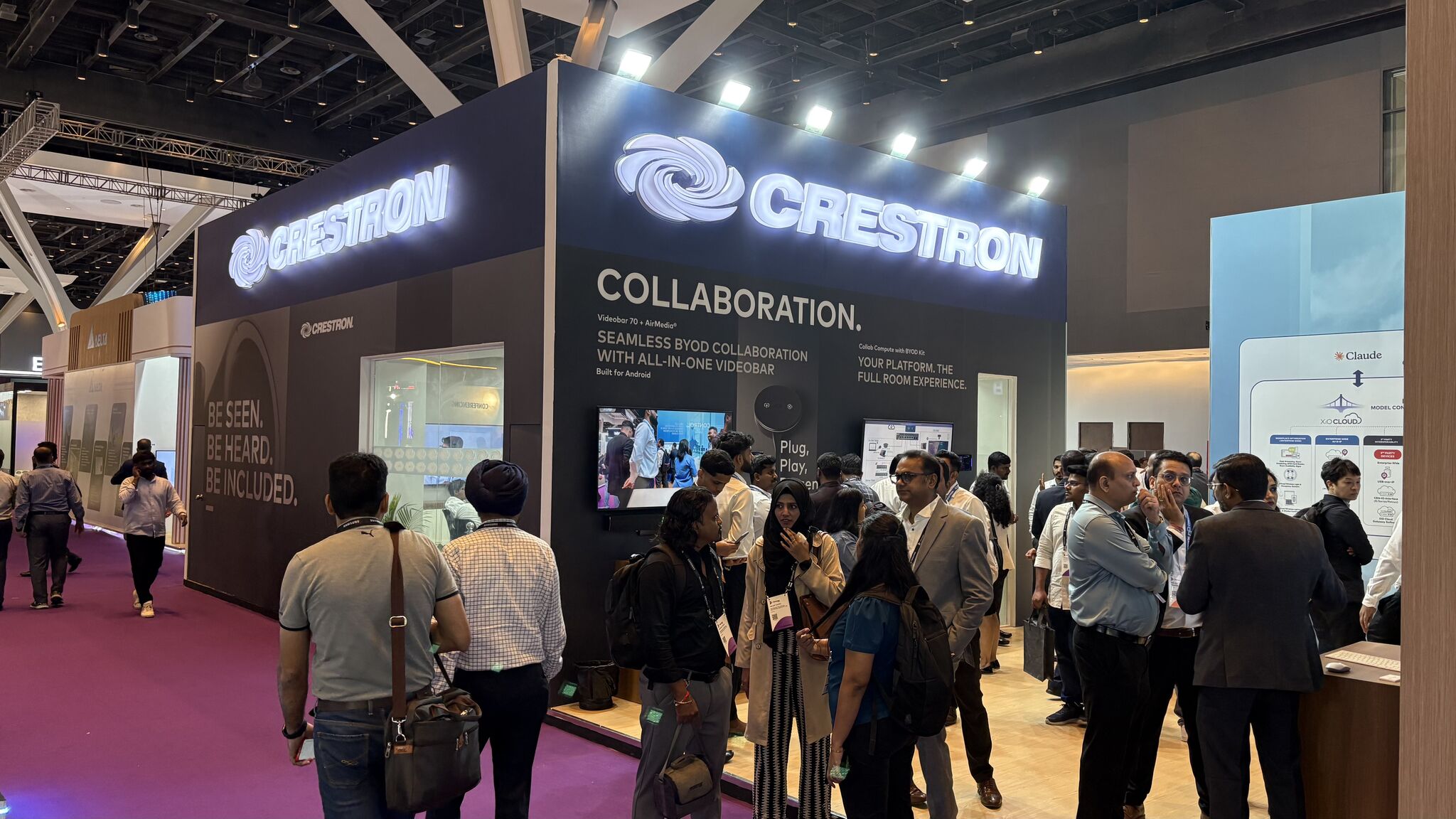
One of the key features at the booth is the India launch of Crestron Collab Compute, a hardware foundation for hybrid meetings. Designed for professional AV and collaboration applications, Collab Compute combines computing capabilities with professional AV connectivity to provide a scalable platform for meeting spaces. It is built on Intel Core Ultra processors with integrated neural processing units (NPUs), providing an AI-ready hardware platform for Microsoft Teams Rooms and Zoom Rooms deployments.
“The workplace is evolving from individual meeting rooms into connected environments where collaboration, communication and intelligent technology need to work seamlessly together. With Collab Compute and our broader portfolio, we are bringing organisations a foundation that is designed not only for the way people collaborate today, but also for how these spaces will evolve,” said Gagan Verma, Vice President – India & SAARC, Crestron. “InfoComm India provides an important platform for us to engage with customers, partners and the wider Pro AV ecosystem and demonstrate how an integrated approach can simplify technology while delivering better experiences.”
Beyond Collab Compute, Crestron is showcasing a selection of its latest solutions spanning collaboration, intelligent video, professional audio, room control and workplace technology. The portfolio includes solutions such as Videobar 70, AirMedia, 1 Beyond i12D, DM-NAX and Automate VX, demonstrating Crestron’s approach to creating connected and flexible environments for modern workplaces.
“India is playing an increasingly important role in Asia’s evolving workplace technology landscape. Organisations are looking for solutions that are flexible, intelligent and scalable, and our presence at InfoComm India reflects Crestron’s commitment to supporting this transformation. The event provides us an opportunity to engage with customers and partners and showcase how integrated technology can create more seamless workplace experiences,” said Jacques Bertrand, Executive Vice President, Asia, Crestron.
The post Crestron Showcases Intelligent AV and Collaboration Solutions at InfoComm India 2026 appeared first on ELE Times.
Nuvoton Launches NuMicro M3351 5V MCU Series for Robotics and Industrial Automation
Nuvoton Technology Corporation, a leading global semiconductor supplier, has introduced the NuMicro M3351 series of 32-bit microcontrollers, featuring an Arm Cortex-M33 core operating at up to 144 MHz and a wide operating voltage range of 2.7 V to 5.5 V. The M3351 series provides a highly integrated 5 V MCU platform for smart appliances, industrial automation, and next generation robotic control.
High-Performance Cortex-M33 Core and Flexible Memory ConfigurationThe NuMicro M3351 series integrates a comprehensive DSP instruction set and a single-precision floating-point unit (FPU), improving execution efficiency for motor control, real-time signal processing, and complex control algorithms. The series offers 256 KB to 1 MB of Flash memory and up to 128 KB of on-chip SRAM. Devices with up to 1 MB of Flash support Dual-Bank operation, ECC, background operation, and Bank Swap, enabling a more flexible and reliable architecture for firmware-over the-air (FOTA) updates.
Select devices also provide up to 64 KB of independent Data Flash with endurance of up to 100,000 program/erase cycles. During Data Flash programming, the MCU can continue executing code from APROM, reducing the impact of parameter storage on real-time control and communication services. By separating firmware from frequently updated data, the system can more efficiently manage calibration parameters, user settings, fault logs, and operating records while reducing the need to reserve APROM space for EEPROM emulation.
High-Resolution Analog Peripherals and Real-Time ControlThe M3351 series integrates a 12-bit SAR ADC with a sampling rate of up to 1.7 MSPS and a 14-bit SAR ADC operating at up to 1.0 MSPS with as many as 16 input channels. It also provides a 12-bit DAC, two analog comparators, up to 24 channels of 16 bit PWM/BPWM, and up to two enhanced quadrature encoder interfaces (EQEI).
Hardware trigger paths among the PWM, ADC, and analog comparator modules reduce CPU workload and improve real-time response, making the M3351 series well suited for closed-loop control applications such as motors, robotic joints, fans, pumps, valves, actuators, and power control systems.
Extensive Connectivity and Hardware-Based SecurityThe M3351 series provides up to two CAN FD interfaces, 10 UARTs, three I²C interfaces, as well as I3C, QSPI, SPI/I²S, USCI, and USB 2.0 Full-Speed Device/Host connectivity.
To address the growing security requirements of connected equipment, the series incorporates Arm TrustZone technology and Secure Boot with SHA-256 and ECDSA-P256 firmware authentication. Select models further integrate TRNG, PRNG, AES-256, SHA-512, and HMAC-SHA hardware functions to strengthen secure boot, firmware authentication, and data protection.
Industrial-Grade Reliability and Comprehensive Development SupportThe M3351 series supports an operating temperature range from -40°C to +105°C and provides robust immunity with ESD HBM protection up to 4 kV and EFT immunity up to 4.4 kV. Its wide 2.7V to 5.5V operating range allows direct operation in common 5V control environments, reducing voltage-conversion requirements and overall system design complexity.
The series is available in package options ranging from the compact QFN33 measuring 5 × 5 mm to the high-pin-count LQFP128 measuring 14 × 14 mm. Nuvoton also provides the NuMaker-M3351KJ development board and Nu-Link debugger, with support for Keil MDK Nuvoton Edition, IAR EWARM, and Visual Studio Code development environments, accelerating product development and deployment across robotics, smart appliances, motor and actuator control, and industrial automation applications.
The post Nuvoton Launches NuMicro M3351 5V MCU Series for Robotics and Industrial Automation appeared first on ELE Times.
Vicor to Showcase Power-Dense DC-DC Converters for Defence Applications at Land Forces 2026
Vicor will demonstrate how high-density power modules enable SWaP compatible power designs for defense applications at the Land Forces International Land Defence Exposition on October 6-8 in Perth, Australia.
Demands of rapid response are driving modern land defense innovation, where electrification is redefining the field mobility strategies and rules of engagement. To meet increasing system capabilities, defense power architecture is moving away from bulky custom subsystems toward a more interoperable, compact, modular building bloc approach.
Vicor enables this shift with high-density power solutions that drastically cut size and weight. Rugged power modules and VITA/SOSA-aligned supplies support the entire delivery network—from high-voltage inputs down to standard MIL-STD 270V and 28V buses. Vicor’s entire high performance portfolio of M-grade products are reliable, rugged and support SWaP specifications.
The post Vicor to Showcase Power-Dense DC-DC Converters for Defence Applications at Land Forces 2026 appeared first on ELE Times.
Laser Parking Assistant Using ToF Technology
Using a brand-new laser distance meter based on ToF technology, we are building a parking assistant for garages and car ports.
The garage space problemCars have grown over the years within the same segment, and while that has given occupants a level of comfort that was unthinkable in the small cars of thirty years ago, it has also forced many drivers to deal with garages and underground car parks that were built and sized for the vehicles of the past. It is not just a matter of width (parking spaces in Italy are often ridiculously small…) but also of length. So more than one driver lines the back wall of the garage with strips of soft material such as foam, because inevitably, to fit the whole car in, one time out of two they hit the back wall.
Electronics, which has shown it has a solution for everything, naturally has one for this problem too; we demonstrate it in this article, where we propose a measurement system based on ST Flight Sense (ToF) technology for proximity detection, implemented by a specific ST chip and fitted with an annular LED display that changes colour according to distance. Something, then, similar to the parking sensors fitted on cars, but this time fixed to the back wall of the parking space.
As we get closer, the LEDs light up green, then gradually turn yellow, then red, and as soon as the distance drops to the minimum they flash red, indicating that you must stop.
The time-of-flight principleTo achieve all this we use a very recent ST product, namely a laser distance meter that can be considered the evolution of the one described in the April 2017 issue, to which we refer anyone who wants to know the fundamentals and the theory of operation of sensors based on the time of flight (ToF) of laser pulses in detail.
To take a measurement, it sends a beam of light against the object or wall to be detected and picks up the reflection from it; this only works if the surface of the object or the wall does not absorb too much of what hits it. The measurement is based on counting the time taken by a pulse to travel from an emitter to the surface of the object to be detected and then back to the sensor; the distance (d) is determined as the product of the propagation speed of the pulse (v) and half of that time (t), according to the relation:
d = v x t/2
The speed of light in air is close to that in a vacuum: 300,000 km/s.
Response times and measurement accuracyThe measurement works like this: when the laser diode is powered, a counter is triggered and is stopped the moment the receiving device is excited by the radiation reflected from the object onto its sensor.
The time counted in this way is affected by the response time of the emitter (the time from when power is applied to when the radiation appears at the emitting surface) and by that of the receiving sensor (the time between when the photons making up the radiation hit the sensitive surface and when the corresponding electrical signal is registered). Another element that introduces tolerance into the measurement is the latency of the counter and of the logic devices in between. Given the very short travel times of the light pulse, these times must be extremely small.
A useful method to limit the error (and so raise accuracy, especially at short distances) is to place a second light sensor facing the emitter (but without covering its emitting surface) so that it detects the light as it leaves; this compensates for both the response delay of the emitter and that of the sensor.
The VL53L0X sensorAfter this introduction let us get to the heart of the project, which consists of the VL53L0X chip, mounted on a breakout board whose schematic we publish, interfaced with a microcontroller that in this specific case is the one on the tiny and essential Beetle; to complete the project we have a ring of NeoPixel LEDs, which will let us give the visual indications required, lighting up in the colour corresponding to the distance detected.
ST FlightSense technologyBefore looking at the complete system, let us spend a moment on the breakout board containing the distance sensor and on the sensor itself, which allows measurements up to 2 m with an accuracy of a few mm. Our sensor, which is based on ST FlightSense technology, integrates in a single SMD package a Photon Avalanche Diode (SPAD) array light sensor, a traditional high-sensitivity ambient light sensor (ALS = Ambient Light Sensor, from 1 Lux to 100,000 Lux) and a class 1 laser diode emitter of the Vertical Cavity Surface-Emitting Laser (VCSEL) type operating at a wavelength of 940 nm, so in the deep infrared.
Independence from the reflection coefficientThe sensor architecture is such that measurements and detections are practically independent of the light reflection coefficient of the surface to be detected, thanks to special circuitry that allows the gain of the receiving stage and the ambient light to be adjusted and very short pulses to be emitted.
On the light sensor side (see Fig. 1) the device incorporates a second light detector that serves to determine the brightness of the environment, so as to obtain a signal that is subtracted, because it is uniform, from the pulse signal coming from the return of the reflected laser pulse; in this way the amplitude of the resulting signal faithfully reflects the distance.
 Fig. 1 The ST sensor chip: on the left you see the block diagram, while the figure on the right highlights, next to the window for the light detector (the lower one), the opening that faces the ambient light sensor.
In other words, it is easy to discriminate the ambient brightness by knowing when the light pulses start and waiting for their arrival, while ambient light is fairly constant.
Emission and reception geometryFig. 2 shows how the sensor works: the pink cone represents the IR light emitted by the laser and in green we see the reception cone of the sensor, with the relevant aperture angles; we note that the reception angle of the photosensor is clearly greater than the emission angle of the laser, which ideally should be zero, since the best solution would be to emit a beam that does not spread, collimated to infinity. In practice a conical beam makes it easier to detect objects, especially small ones.
 Fig. 2 Structure of the ST sensor: the cone of light emitted by the LED is narrower than the aperture of the SPAD sensor.
Eliminating the reflected light is essential in this case, not so much because of the level of disturbance it superimposes on the return signal, but rather for the calculation of the time of flight of the light pulse, since the wave reflected inside the glass would arrive before the light reflected by the object whose distance is being measured, causing a measurement error on the low side (the measured distance would be shorter).
Detection with the VL53L0XLet us now see, with the help of Fig. 3, how detection by the VL53L0X takes place: the laser diode (Emitter) emits periodic light pulses, part of which is reflected by the Target Object (the object or wall whose distance is to be measured) and returns to the sensor; by synchronising the emission with the waiting for the pulses, it is possible to remove the disturbance caused by ambient brightness, raising the sensitivity of the device. The substantial difference between the VL53L0X and typical IR proximity meters is that the latter are based on the intensity of the reflected wave, which makes them unreliable because it depends on the reflection coefficient of the surface of the object to be detected.
 Fig. 3 Schematic of how the VL53L0X family of devices works.
The peculiarity of the detector diode, that is the Single Photon Avalanche Diode, is that it works in reverse bias in the portion of its characteristic corresponding to the onset of the avalanche effect: keeping the diode at an anode-cathode voltage close to the breakdown voltage, when the surface is struck by light, the first photon of that light triggers conduction by avalanche effect and the current increases sharply, then drops to zero when the voltage falls below the breakdown voltage. At this point another photon is needed to trigger conduction. By arranging an array of these diodes it is possible to count photons.
Schematic of the breakout board Schematic of the breakout board built around the VL53L0X sensor.
Let us now take a look at the breakout board containing the VL53L0X sensor, where besides the chip we find a low drop-out linear voltage regulator (U1) and a MOSFET adapter for the I²C-Bus interface, useful for shifting the 0/2.8 V logic levels of the chip to adapt them to the standard TTL levels of boards with traditional logic and of Arduino.
The I²C level shifterTo explain how the shifter works, let’s start with the clock, which on the U2 side is routed to the line of pin 10, while towards the connection pin-strip it is tied to SCL (both lines have a pull-up resistor): when the SCL of the connector is at a logic high level, the protection diode inside the MOSFET (placed between drain and source) is reverse biased because the source is negative (it sits at 2.8 volts) with respect to the drain (which is held at 5 volts by R5), and even though the pulse does not reach the SCL of U2, the latter is at logic 1. Conversely, when the SCL contact of the pin-strip is at logic zero (0 V), the MOSFET is still off (because its gate is biased at 2.8 volts) but its protection diode conducts, since the source is at 2.8 V while the cathode is at zero, so the low level on SCL pulls pin 10 of the VL53L0X down to logic zero (0.6 V to be exact). The SCL channel is unidirectional, so the opposite situation does not arise, that is, U2 receives the clock from the host.
Let’s move on to SDA, analysing the case where the host is sending data: when SDA is at logic zero, the protection diode of Q2 conducts and pulls the source, and with it pin 9 of U2, down to 0.6 V; on the other hand, when it is at 5 volts, both the MOSFET and the diode are off, so the SDA of the VL53L0X is brought to 2.8 V (high level) by the pull-up resistor R7.
If instead it is U2 that is transmitting, when it brings its own pin 9 to logic zero the MOSFET Q2 conducts between drain and source, because its source is at zero volts while the gate is at 2.8 V, so its drain current pulls the SDA of the connector down to about 0 V, due to the drop across the pull-up resistor R6; conversely, when pin 9 of U1 is at a high level (2.8 V) the source and gate are at the same potential and the MOSFET stays off, letting the pull-up resistor R6 hold the SDA line going to the pin-strip at logic 1 (but at 5 volts).
The voltage regulatorAs for the voltage regulator, it is a MIC5504-2.8YM5-TR from Micrel, that is, an LDO with a 2.8 V output (supplied at the input between 2.5 and 5 V) capable of delivering 500 mA of current, packaged in a SOT-23 case and with a minimum voltage drop of 160 millivolts between the IN and OUT pins; it is very stable over temperature and integrates short-circuit protection at the output and over-temperature protection, as well as input reverse-polarity protection.
The chip can be put into shutdown by bringing its EN pin to logic zero.
I²C communication and GPIO configurationCommunication with the host device, typically a microcontroller, takes place over the I²C-Bus formed by the SCL (5) and SDA (6) pins, respectively the clock and the bidirectional data channel; through the bus (which runs at 400 kHz) it is possible to set operating modes, sensitivity and so on, but also to read the measurement result. Regarding operating modes, it should be said that the device can take a measurement at a settable rate, or on request (a mode that helps optimise consumption, which comes largely from switching on the laser).
Before concluding the description of the schematic, let’s spend a moment on the GPIOs of the VL53L0X, which can be configured through specific commands sent over the I²C-Bus; the setting for our project is contained in the dedicated library that can be downloaded together with the other project files. In it:
- GPIO0: changes state when acquisition is complete and can be used to tell the Host microcontroller that it can read the measurement;
- GPIO1, if brought to GND, puts the ST device into standby; once it is in that condition, U1 can be reactivated by sending it again over the I²C-Bus the configuration required for the measurement (so simply bringing the GPIO back to a high level is not enough).
The VL53L0X is powered through the AVDD (positive) and GND (ground) pins for the receiving section and AVDD_VCSEL and AVSS-VCSEL for the laser diode.
The VL53L0X management library can be downloaded, along with the other project files, from https://github.com/pololu/vl53l0x-arduino. To use it, after downloading it you must copy the folder contained in the .zip file into the “libraries” directory where the Arduino environment is installed. The same goes for the library that manages the Neopixel ring.
The parking assistantWell, now that you know everything about the breakout board, let’s see, with reference to the wiring diagram, how our system was built. The small Beetle is enough for us because we only use four I/Os, namely two for the I²C-Bus with which the little Arduino talks to the breakout board and one for the data channel needed to drive the neopixel ring, which specifically is a RING16NEOPIXEL, made up of 16 RGB neopixel LEDs (we have already used these special “smart” LEDs several times in the past). Everything is powered by the voltage applied to the Beetle.
The firmwareAs for the firmware side, the project is managed with the sketch (VL53L0X_Garage_v2), the most relevant portion of which you will find in Listing 1; it loads the VL53L0X and neopixel ring management libraries, after initialising the serial connection, and then loads the I²C-Bus library to communicate with the breakout board, then starts polling the latter cyclically and listening for the corresponding data; the same sketch will send the data on the detected Lux and the distance from the object to the serial port opened for Arduino. The sketch also initialises the line (pin 11) used to drive the LED ring.
Note that the sensor has a default range of 1.2 metres; to raise it to the declared maximum of 2 metres you need to configure it with a dedicated command. It should also be considered that the two metres are reached indoors and not outdoors. The less light there is, the more accurate the reading will be, but that matters little to us because the system will normally be used in garages and in covered and underground car parks.
The sketch is written for a 16-LED ring, but there is nothing stopping you from using a larger one or several combined together: to do so you need to modify the statement #define PIXEL_COUNT 16.
The colour thresholdsWhen the vehicle enters, it is detected at a distance of at least 1.2 metres (the value set in the sketch) and the neopixel ring automatically lights up green, one LED at a time until all the LEDs are on. As the car gets closer to the wall (to the sensor), the colour of the light indicator changes accordingly; to be exact, the light is:
- green: between 120 and 60 cm;
- yellow: between 60 and 30 cm;
- red: between 30 and 15 cm;
- flashing red: below 15 cm.
From green to yellow light the LEDs fade out gradually.
If the vehicle stops, since the same position keeps being detected (the ring stays on the same colour), after a certain number of cycles (the MAX_ON variable in the sketch) the indicator turns off. Currently in the sketch the turn-off time is set to about 30 seconds, that is, “MAX_ON * (DELAY_CYCLE +100)” where 100 is a fixed delay present in the various cycles. As soon as a change in distance is detected, the firmware reactivates the system. This trick makes it possible to limit power consumption to what is strictly necessary.
Long Range and shutdownIt should be pointed out that the firmware is set up for the ranges given above, but for greater accuracy and to avoid false readings, the sensor’s Long Range mode (up to 2 metres) has not been enabled; this way the maximum range will be 1.2 m, but that is more than a valid value in a garage. If you wanted to enable Long Range, you would only need to remove the comment from the statement “#define LONG_RANGE” and then reload the firmware onto the board.
Note that the firmware provides for the possibility of managing the shutdown of the breakout board through the statement int pwrPin = 13, which sets pin 13 to act on the SHD line.
Listing 1#include <Wire.h> #include <VL53L0X.h> #include <Adafruit_NeoPixel.h> #define PIXEL_PIN 11 //Pin used to drive the NeoPixel #define PIXEL_COUNT 16 //Number of NeoPixels to manage //#define LONG_RANGE //Enable if you want the ToF to detect up to 2m //(not recommended in bright environments) instead of //1.2m (recommended for indoor use) VL53L0X sensor; Adafruit_NeoPixel strip = Adafruit_NeoPixel(PIXEL_COUNT, PIXEL_PIN, NEO_GRB + NEO_KHZ800);
int val_max = 60;//Brightness value (up to 255)
int distance = 0;//distance value read from the ToF
int num_R = 0; //Number of times the red colour turns on in the same range
int num_Y = 0; //Number of times the yellow colour turns on in the same range
int num_G = 0; //Number of times the green colour turns on in the same range
int num_led_on = 0; //Convenience variable used by some effects
//If the same colour stays active for MAX_ON cycles, the
//indicator turns off. The time is roughly defined by //MAX_ON * (DELAY_CYCLE + 100ms) (seconds)
int const MAX_ON = 200;
int const ALARM1 = 150; //Alarm threshold 1
int const ALARM2 = 300; //Alarm threshold 2
int const ALARM3 = 600; //Alarm threshold 3
int const ALARM4 = 900; //Alarm threshold 4
int const ALARM5 = 1200; //Alarm threshold 5
int const DELAY_CYCLE = 50; //Pause time in ms
int const DATO_OK = 4; //Number of readings that must be valid to
//turn the indicator on. It is needed to remove
//possible spikes caused by light
void setup()
{
strip.begin();
strip.show(); //Pixel initialisation
Serial.begin(9600);
Wire.begin();
sensor.init();
sensor.setTimeout(500);
#if defined LONG_RANGE
//lower the return signal rate limit (default is 0.25 MCPS)
sensor.setSignalRateLimit(0.2);
//increase laser pulse periods (defaults are 14 and 10 PCLKs)
sensor.setVcselPulsePeriod(VL53L0X::VcselPeriodPreRange, 18);
sensor.setVcselPulsePeriod(VL53L0X::VcselPeriodFinalRange, 14);
#endif
sensor.startContinuous();
}
void loop()
{
distance = sensor.readRangeContinuousMillimeters();
if (distance < ALARM1) //If distance is less than 15cm turn on the red colour
{
if (num_R<MAX_ON)
{
num_R=num_R+1;
num_Y=0;
num_G=0;
//Immediate turn-on because the obstacle is too close
Colore(1,2,distance,ALARM1,0);
}
}
//If distance is between 15cm and 30cm turn on the yellow colour
if ((distance > ALARM1) && (distance <= ALARM2)) {
if (num_R<MAX_ON)
{
num_R=num_R+1;
num_Y=0;
num_G=0;
//Turn the LED on only with a DATO_OK number of readings in the same range
if (num_R>=DATO_OK) Colore(1,1,distance,ALARM2,ALARM1);
}
}
//If distance is between 30cm and 60cm turn on the yellow colour
if ((distance > ALARM2) && (distance <= ALARM3))
{
if (num_Y<MAX_ON)
{
num_R=0;
num_Y=num_Y+1;
num_G=0;
if (num_Y>=DATO_OK) Colore(2,1,distance,ALARM3,ALARM2);
}
}
//If distance is between 60cm and 90cm turn on the green colour
if ((distance > ALARM3) && (distance <= ALARM5))
{
if (num_G<MAX_ON)
{
num_R=0;
num_Y=0;
num_G=num_G+1;
if (num_G>=DATO_OK) Colore(3,4,distance,ALARM5,ALARM3);
}
}
if (distance > ALARM5) //If distance is greater than ALARM5 turn the indicator off
{
num_R=0;
num_Y=0;
num_G=0;
Colore(0,1,distance,0,0);
}
if ((num_R>=MAX_ON) || (num_Y>=MAX_ON) || (num_G>=MAX_ON))
{
Colore(0,1,distance,8000,ALARM5);
}
if (sensor.timeoutOccurred()) { Serial.print(” TIMEOUT”); }
delay(DELAY_CYCLE);
}
//Sets the colour and the turn-on mode
void Colore(int col, int mode, int dist, int alarm_MAX, int alarm_MIN)
{
uint32_t R;
uint32_t G;
uint32_t B;
switch(col)
{
case 0: //All Off
R=0;
G=0;
B=0;
break;
case 1: //Red
R=val_max;
G=0;
B=0;
break;
case 2: //Yellow
R=val_max;
G=val_max/2;
B=0;
break;
case 3: //Green
R=0;
G=val_max;
B=0;
break;
}
switch(mode)
{
case 1:
num_led_on=0;
ColorOn(strip.Color(R, G, B)); //Steady on
break;
case 2:
num_led_on=0;
ColorBlink(strip.Color(R, G, B)); //Blinking colour
break;
case 3:
ColorCircleSingle(strip.Color(R, G, B)); //Cyclic turn-on
break;
case 4:
ColorDistance(strip.Color(R, G, B),dist,alarm_MAX,alarm_MIN);
break;
}
}
//Gradual turn-on of the colour based on the distance you are at
void ColorDistance(uint32_t c, int dist1, int almax, int almin)
{
double val1;
double val2;
uint16_t i;
val1=almax-almin;
val1=val1/PIXEL_COUNT;
val2=dist1-almin;
val2=almax-val2;
val2=val2-almin;
val2=val2/val1;
if (num_led_on==0)
{
for(i=0; i<strip.numPixels(); i++) //turn all the LEDs off
{
strip.setPixelColor(i, strip.Color(0, 0, 0));
}
strip.show();
//Turn on only the LEDs based on distance (the closer to the wall, the
//greater the number of LEDs turned on)
for(i=0; i<val2; i++)
{
strip.setPixelColor(i, c);
}
strip.show();
delay(100);
}
}
Assembly plan The assembly plan for the S1341 breakout board.
R1: 47 kohm (0201)
R2,R3: 1 kohm (0201)
C1: 100 nF ceramic (0201)
Q1: SI2302DS
Q2: BCR112
D1: BAS316
D2: yellow LED (0201)
U1: PIC10F320T-I/OT (MF1341)
Miscellaneous:
- 6-way male pin strip
- 3-way male pin strip
- 2-way male pin strip
- S1341 printed circuit board (16 x 11 mm)
 Wiring diagram of the breakout board, Beetle and LED ring.
We wrap up this article with the build; we start from the breakout board (given the complexity of the assembly we decided to make it available already assembled…) which begins with the preparation of the double-sided printed circuit board, for which the copper-side traces are available for download.
SMD preparation and solderingOnce the board has been etched and drilled, you need to move on to assembly, which requires a minimum of equipment, since the components are surface-mount and the ToF sensor comes in a GAL package with contacts underneath. So get yourself a fine-tip soldering iron, some solder wire no more than 0.5 mm in diameter, some thin flux paste and a small brush to spread it, plus tweezers to handle the components and a magnifying lens to check that they are first positioned and then soldered correctly. Desoldering braid will also come in handy to remove any excess solder, which could short-circuit adjacent pins or pads.
Soldering the VL53L0X requires a hot-air station. Assembly should start with the VL53L0X, tinning and then coating the corresponding pads on the board with flux; then, if you have a heating plate, suspend the PCB at a suitable distance above it, otherwise heat the board from the side opposite the components with air at 260 °C for about ten seconds, then rest the board on a table (not a plastic one…) and, after positioning the chip with tweezers well centred in its holes, heat it with the hot-air jet until you see it “sink” onto the pads. At that point remove the hot air and switch the station off.
Now move on to the resistor and capacitor chips, then place the voltage regulator well centred on its pads (spread with flux paste) and oriented as shown in the assembly plan; carry on with the MOSFETs and finish with the pin strip that provides the connections to the Beetle.
When using the flux, be careful not to dirty the holes on the surface of the VL53L0X, which must stay free and clean, otherwise the distance detection and measurement system will malfunction. Once assembly is complete, use the magnifying lens to check that all the components are in place, well soldered (good solder joints are shiny, while dull ones risk oxidation and intermittent contact…) and centred on their pads; also check that there are no solder whiskers creating short circuits.
Final assemblyOnce the sensor breakout board is built you have to connect it to the Beetle as shown in the wiring diagram and then connect the Beetle to the LED ring; you will power the whole thing by supplying a stabilised 5V only to the + and – pads of the small Arduino, since from there the 5V will then reach both the breakout board and the Neopixel ring.
For the project we made a 3D-printed enclosure in PLA, or rather two enclosures to be joined by a rectangular PVC conduit for electrical installations. In the upper enclosure you will fit the display made up of the Neopixel LED ring and the Arduino Beetle, and in the lower one the breakout board; this latter “body” should be positioned at the typical height of the vehicle’s bumper, so as to detect the distance that matters most to us, namely that from the most protruding part. That done, you are ready to enjoy your assistant.
Related productsThe post Laser Parking Assistant Using ToF Technology appeared first on Open Electronics.
Gartner Forecasts Global AI Spending to Reach $2.7 Trillion in 2026, Up 49.5%
Worldwide spending on AI is forecast to total $2.7 trillion in 2026, a 49.5% increase year-over-year, according to Gartner, Inc., a business and technology insights company.
“Demand for AI infrastructure (including AI-optimized IaaS, AI-optimized servers, AI network fabric, AI processing semiconductors and devices) to support anticipated future workloads remains strong and inelastic to pressures from memory related pricing increases,” said John-David Lovelock, Distinguished VP Analyst at Gartner. “The buildout of AI data center capacity is the largest infrastructure project humanity has even undertaken. The capacity growth from hyperscalers and service providers purchasing AI-optimized servers will continue to be the largest single area of spending.”
In the software market, vendors across different software types are rapidly embedding agentic AI within their existing products to maintain relevance in the market and defend against new cross-functional agents (see Table 1). With GenAI firmly in the Trough of Disillusionment in 2026, enterprises are using these simpler embedded AI features from their incumbent software providers to grow operational efficiency and automate workflows, improve customer engagement and enhance decision making.
Table 1: Worldwide AI Spending by Market, 2025-2027 (Millions of U.S. Dollars)
| Market | 2025 | 2026 | 2027 |
| AI Services | 434,046 | 576,481 | 745,655 |
| AI Cybersecurity | 25,920 | 51,347 | 85,997 |
| AI Software | 288,168 | 461,637 | 656,353 |
| AI Agents and Assistants | 16,481 | 29,219 | 65,472 |
| Generative AI Models | 13,021 | 28,266 | 51,620 |
| AI Platforms for Data Science and Machine Learning | 19,405 | 26,445 | 35,552 |
| AI Application Development Platforms | 6,885 | 9,541 | 12,478 |
| AI Data | 826 | 3,126 | 6,480 |
| AI Infrastructure | 981,920 | 1,484,397 | 1,977,685 |
| Total AI Spending | 1,786,671 | 2,670,460 | 3,637,292 |
“Meanwhile enterprises are turning to service providers less often to help them manage the business transformation, and more often for the smaller indirect projects to exploit AI features of their incumbent software system,” said Lovelock. “The risks associated with vendor lock-in, data sovereignty, and run-away costs are not deterring buyers from adopting these proprietary capabilities. The combination of transformation and indirect projects are forecast to drive a $1.2 trillion opportunity in AI services by 2030.”
Near-Term Outlook ChangesThe short-term outlook for AI application development platforms has increased from 28% growth in 2026 in the previous forecast to 39% in this quarter’s forecast, as enterprises, software providers and services firms seek to develop custom AI applications tailored to their individual needs. Enterprises are looking to their providers to help them manage their costs and embed usage tracking into their workflows to evaluate success. For model providers, the pressure to offer more cost-efficient models that are aligned to enterprise use cases is opening a small but growing opportunity for domain-specific language models (DSLMs). As a result, the 2026 growth rate for generative AI models has increased from 110% growth in the previous forecast to 117% growth in the current forecast.
Long-Term Outlook ChangesIn the current forecast, Gartner has separated cross-functional agents and assistants from AI software and added consumer agents and assistants into the AI spending forecast to better show the emerging opportunity in this area.
The post Gartner Forecasts Global AI Spending to Reach $2.7 Trillion in 2026, Up 49.5% appeared first on ELE Times.
Сторінки



