


Збирач потоків
EDOM Accelerates Edge AI Deployment with NVIDIA Technologies
EDOM Technology, Asia’s best solutions provider, today announced an expanded collaboration with NVIDIA to help enterprises accelerate Edge AI adoption by integrating the NVIDIA Edge AI platform, open-source models, and system optimization technologies. The collaboration enables organizations to lower the barriers to deploying large AI models while reducing overall deployment costs.
As generative AI rapidly evolves from proof-of-concept to real-world applications, enterprise priorities are shifting. Rather than simply pursuing larger AI models, organizations are increasingly focused on running AI reliably on existing hardware platforms, accelerating deployment, and maximizing return on investment. Across industries from smart manufacturing and autonomous robotics to healthcare, Edge AI has become a key driver of digital transformation where efficient deployment is critical to successfully bringing AI projects into production.
The way enterprises adopt AI is also changing. Instead of building models from scratch, organizations are increasingly leveraging mature foundation models and open-source AI ecosystems to accelerate development, followed by application specific optimization and deployment. However, as AI models continue to grow in capability, several deployment challenges such as memory capacity, inference performance, and system integration have become major hurdles.
EDOM addresses these challenges by combining the NVIDIA Jetson platform with NVIDIA JetPack, NVIDIA CUDA, NVIDIA TensorRT, NVIDIA Jetson AI Lab, and leading open-source AI models and inference frameworks. The company delivers a comprehensive portfolio of services spanning platform selection, model integration, model quantization, memory optimization, and system validation. This end-to-end approach enables enterprises to maximize hardware resource utilization, reduce deployment costs, and shorten the journey from proof of concept (PoC) to production.
A notable example is NVIDIA Reachy Mini Jetson Assistant, which demonstrates how Headless Mode, NVIDIA Cosmos-Reason2 open VLMs, model quantization, and optimized inference frameworks enable multimodal AI workloads—including vison- language reasoning, Speech-to-Text (STT), and Text-to-Speech (TTS)—to run simultaneously on the NVIDIA Jetson Orin Nano 8GB platform. This showcases how software and system optimization can efficiently execute multiple AI models and reduce memory footprint on resource-constrained edge devices. Similar architectures are increasingly being adopted across smart manufacturing, autonomous robotics, and healthcare applications, supporting use cases such as production line inspection, intelligent vision systems, voice-enabled interaction, and autonomous decision-making. By performing AI inference directly on edge devices, organizations can achieve low-latency performance while enhancing data security and operational efficiency.
“Generative AI has entered the stage of real-world deployment,” said Jeffrey Yu, CEO of EDOM Technology. “Today, the biggest challenge for enterprises is no longer finding AI models; it’s successfully deploying AI into products and operational environments. The success of an AI project depends not only on hardware performance, but also on deployment efficiency, system integration capabilities, and overall return on investment. EDOM’s role extends beyond supplying platforms and components. We help customers integrate NVIDIA technologies, open-source AI models, and system optimization strategies to accelerate time-to-market, reduce deployment risks, and enable AI to deliver measurable business value.”
Backed by years of expertise in Edge AI and embedded system integration, EDOM provides end-to-end solutions encompassing selections powered by NVIDIA technologies, open-source AI models integration and application optimization, hardware design, and system deployment. The company has successfully enabled Edge AI applications across smart manufacturing, autonomous robotics, healthcare, smart retail, and smart city initiatives. Looking ahead, EDOM will continue collaborating with NVIDIA and the open-source AI community to help enterprises overcome the challenges of deploying large AI models, accelerate the transition from proof of concept to large-scale deployment, and transform AI innovation into tangible value across the industry value chain.
The post EDOM Accelerates Edge AI Deployment with NVIDIA Technologies appeared first on ELE Times.
Uttar Pradesh Emerges as India’s Biggest Electronics Hub, Producing 65% of the Nation’s Mobile Phones
Uttar Pradesh has emerged as India’s leading electronics manufacturing hub, producing nearly 65% of the country’s mobile phones. Driven by strong investments, industry-friendly government policies, and the rapid expansion of manufacturing facilities, the state has become a major centre for electronics manufacturing and mobile phone production.
Since 2014, UP has been a hotspot for electronic manufacturers, including domestic and international ones to invest particularly in the Noida-Greater Noida-Yamuna Expressway corridor. Global big manufacturing smartphones, as also their component suppliers, have built huge manufacturing units in the area and put up a complete electronics manufacturing value chain. The state government says it accounts for roughly 65% of all mobile phones being manufactured in the country and is India’s biggest base for smartphone production.
Multiple efforts by both central and state governments have assisted the growth of the electronics sector in the state of Uttar Pradesh. At the national level, policies like the Production Linked Incentive (PLI) Scheme for large electronics manufacturing incentives; the setting up and scaling of production capacities in India, whereas the electronics manufacturing policy issued by the state offers supplemental incentives, enhanced infrastructure, and business ease reforms.
The proactive actions of the Uttar Pradesh government to streamline approvals, build an efficient logistics infrastructure, boost investor confidence, and encourage (foreign direct investment) FDI have positioned the state as a prominent investment destination for the global electronics sector.
While these efforts should result in significant acceleration of manufacturing and investment in UP, the state has a lot of work ahead of itself in achieving sustained future growth. Increasing domestic value addition; further ramping up production of semiconductors and components; creating an ecosystem of highly skilled personnel; and upgrading research and development to enhance in-house R&D is crucial for a long-term plan. To stay competitive globally, UP will also need to make priority investments, to ensure availability of dependable power supply, a world-class logistics system, and highly advanced manufacturing technologies.
The post Uttar Pradesh Emerges as India’s Biggest Electronics Hub, Producing 65% of the Nation’s Mobile Phones appeared first on ELE Times.
Rapid scale-up in data center: The case for distributed optical circuit switching

AI infrastructure is moving from server-scale acceleration to multi-rack supernodes that must behave like a single, highly available computer. Distributed optical circuit switching offers a practical way to extend scale-up fabrics with lower latency, lower power, flexible topology control, and limited disruption to existing data center architecture.
AI data centers are entering a phase where the hardest problem is not simply building a faster accelerator. It’s keeping thousands of accelerators fed, synchronized, and available as one machine. Training frontier models, serving long-context inference, and running agentic workloads all create a similar demand: more devices must communicate over longer distances without allowing the network to dominate cost, latency, power, or reliability.
That changes the definition of scale-up. It’s no longer only the set of links inside a server or rack. Increasingly, scale-up must span multiple racks while preserving the low-latency behavior programmers expect from a tightly coupled system.
Nvidia has framed the issue in similar terms, noting that as AI factories reach “extreme scale,” networking infrastructure “must be reinvented to keep pace.” The company’s recent silicon photonics announcements focus on exactly the metrics now becoming critical in AI infrastructure: power efficiency, signal integrity, resilience, and deployment speed.
That emphasis reflects a broader industry shift. The bottleneck is no longer just whether a link can move bits from one endpoint to another. It’s whether the entire fabric can support large, tightly synchronized accelerator domains while reducing power, limiting failure points, and remaining practical to deploy and service.
Copper has been the default for scale-up because it’s familiar, low latency, and economical at short reach, but physics is becoming less forgiving as per-lane data rates rise. Longer copper paths increase insertion loss and signal-integrity burden; thicker wires help the signal but work against density, airflow, and manufacturability.
Rack-scale cable trays become difficult to assemble and service, and a failure may require replacing large mechanical units rather than a small module. Retimers, equalization, and more complex board design can extend the life of copper, but they do not remove the underlying reach-density-power tradeoff.
Traditional pluggable optics solve part of this problem. They move data farther with less distance penalty than copper and are widely deployed in scale-out networks. But a scale-up fabric is different from a scale-out Ethernet fabric. Scale-up traffic often has stricter latency, synchronization, and collective-communication requirements, and in emerging architectures may carry memory-semantic traffic rather than ordinary packetized network traffic.
In that environment, the raw specifications of an optical link alone are not sufficient. The fabric also needs deterministic paths, fast reconfiguration, high serviceability, and smaller, more containable failure domains.

Figure 1 Next-generation scale-up and scale-out solutions extend the limits of traditional electrical interconnect and pluggable optical modules. Source: Lightelligence
Co-packaged optics (CPO) is an important long-term solution, but it’s not a simple drop-in replacement for today’s data center designs. Bringing optical engines into or near the package changes the thermal, packaging, manufacturing, serviceability, and qualification model. Recent industry discussions around CPO focus heavily on these operational issues: how to manufacture high-yield optical assemblies, make optical interfaces field-serviceable, and manage light sources and redundancy at scale.
Nvidia’s recent Spectrum-X Ethernet Photonics announcements also show where early CPO commercialization is gaining traction: scale-out and scale-across AI-factory networking. Scale-up CPO will follow, but it asks a different question: how do we preserve the behavior of a tightly coupled compute domain while changing the physical medium underneath it?
This is where distributed optical circuit switching, or dOCS, becomes important. Rather than concentrating the switching function in precious rack space, a dOCS architecture distributes compact silicon-photonic switching elements close to servers, GPU trays, or XPU clusters. This improves compute density by eliminating the switch chassis.
The goal is to keep data in the optical domain from port to port through the switch path, reducing unnecessary optical-electrical-optical conversions and avoiding the power and cost burden of very large centralized electrical switch ASICs. In practical terms, dOCS treats the scale-up network less like a fixed cable plant and more like a configurable optical fabric.

Figure 2 A distributed optical circuit switch (dOCS) integrates the optical interconnect and switching functions into one compact module. Source: Lightelligence
The distinction matters. A centralized switch can become expensive, power-intensive, and operationally painful as scale-up domains grow. It can also create a large failure domain. A distributed optical switch breaks the switching function into smaller modules, shrinking the blast radius of any one failure and enabling more granular service.
In one described implementation, the dOCS module integrates optical interconnect and optical circuit-switching functions in a compact module built around silicon photonics, controller, driver, and receiver circuitry. The architecture is intended to support millisecond-level failover, including substitution of a hot-standby GPU when a device fails.
For AI workloads, the value of that reconfigurability is not only resilience, it’s also topology control. Different phases of training and inference stress the fabric differently.
Dense all-reduce operations, mixture-of-experts routing, retrieval, key value (KV)-cache movement, and pipeline-parallel execution do not all benefit from the same topology. A circuit-switched optical layer can expose topologies such as ring, mesh, or dragonfly and allow the cluster manager to adjust the fabric according to specific workload-parallelism requirements.
Recent dOCS-based supernode work has described real-time topology reconfiguration and elastic expansion beyond 500 GPUs in a single logical domain. The broader architectural point is more important than the exact number: the network should become a schedulable resource, not a static constraint.
This also helps explain why dOCS is especially relevant to certain architectures. A supernode is not just a cluster with a marketing label. It is a tightly interconnected group of GPUs or other accelerators that attempts to behave like one large compute unit. In that context, effective model FLOPs utilization depends on how much time accelerators spend computing rather than waiting.
Optical scale-up links can extend reach across racks, while circuit switching can create predictable paths for high-volume collective traffic. The result is not simply more bandwidth on a datasheet; it’s a path to higher sustained utilization.
The same argument applies to memory. AI systems are increasingly constrained by memory capacity, memory bandwidth, and the location of memory relative to compute. High-bandwidth memory (HBM) on the accelerator remains essential, but it’s finite and expensive. Long-context inference and agentic workloads amplify the pressure by generating large KV caches and preserving more state across interactions.
CXL is important because it provides cache-coherent connectivity for processors, memory expansion, and accelerators, enabling resource sharing with lower software complexity. But coherent memory fabrics still need physical reach. Optical PCIe/CXL links and reconfigurable optical switching can help move memory from a stranded local resource toward a pooled resource available across boards, servers, and racks.
The practical advantage of dOCS is that it creates an intermediate deployment path. Data center operators do not need to redesign every server, change every protocol, or wait for full CPO maturity before gaining optical reach and switching flexibility in the scale-up domain. A dOCS-based fabric can be designed to remain protocol agnostic at the physical layer, supporting multiple higher-level fabrics while changing the transmission medium and switching mechanism underneath.
That matters because AI data centers are heterogeneous. They include GPUs, CPUs, XPUs, switches, storage, memory expansion devices, and management controllers sourced from multiple vendors and refreshed on different schedules.

Figure 3 As shown in this example, the dOCS architecture offers a practical advantage by creating an intermediate deployment path. Source: Lightelligence
A sensible roadmap is therefore not copper versus CPO, or pluggables versus CPO. It’s a staged migration. Linear pluggable optics can address immediate reach and power issues with limited architectural change. Distributed optical circuit switching can add fabric-level reconfiguration, availability, and scale-up reach.
Near-packaged optics can shorten electrical traces and improve density. CPO optics can eventually move optical I/O directly beside GPUs or switch ASICs for the highest bandwidth density and lowest electrical loss. Each step moves optics closer to the compute, but each step should also preserve serviceability and operational practicality.
The AI infrastructure industry is learning a familiar lesson from earlier computing transitions: the winning technology is rarely the one with the most elegant device physics alone. It’s the one that fits into systems, software, manufacturing, and operations at the right time.
The dOCS architecture fits that requirement because it attacks a real bottleneck now. It extends scale-up beyond the practical limits of copper, avoids inefficiencies of repeated electrical conversion, supports flexible accelerator-fabric topologies, and improves system uptime by localizing failures and rapidly rerouting traffic or switching to standby resources when hardware fails.
The future data center will almost certainly use several optical technologies at once: pluggable optics, linear drive optics, near-packaged optics, CPO, optical I/O chiplets, CXL-enabled memory fabrics, and optical circuit switches. The case for dOCS is that it gives operators a rapid-deploy scale-up option while the rest of the optical roadmap matures.
For AI infrastructure, that may be the most important kind of innovation: not a clean-sheet replacement for the data center, but a way to make the next supernode larger, more efficient, more available, and easier to deploy than the last one.
 Maurice (Mo) Steinman is senior VP and U.S. GM at Lightelligence. He has enjoyed a 40-year career in the semiconductor industry, working for such companies as Digital, Compaq, HP, Intel and AMD, where he held the title of Senior Fellow before joining Lightelligence. Steinman has expertise in SoC architecture, SoC interconnect, memory subsystems, and energy management.
Related Content
- Optical switches primed for test debut
- The advent of co-packaged optics (CPO) in 2025
- Building Optical Control Planes: Challenges and Solutions
- Where co-packaged optics (CPO) technology stands in 2026
- Overcoming interconnect obstacles with co-packaged optics (CPO)
The post Rapid scale-up in data center: The case for distributed optical circuit switching appeared first on EDN.
Global Semiconductor Equipment Sales Projected to Reach Record $229.5 Billion in 2028
Global sales for semiconductor manufacturing equipment are expected to set another all-time record by 2028, hitting $229.5 billion. This is due to continued spending in artificial intelligence, leading-edge logic, advanced memory, high bandwidth memory (HBM), testing and advanced packaging. The findings are according to the latest forecasts from SEMI in its Mid-Year Total Semiconductor Equipment Forecast – OEM Perspective.
SEMI expects global semiconductor manufacturing equipment sales to rise 23.2% to $165.9 billion in 2026 and continue growing through 2028, marking five consecutive years of growth. The market is entering a new growth cycle, driven mainly by AI- related investment in semiconductor manufacturing and capital spending.
Demand for advanced logic chips and High Bandwidth Memory (HBM) is increasing as the use of AI and HBM-based technologies expands. These applications require increasingly advanced manufacturing processes and more complex chip designs.
According to market analysis, wafer fabrication equipment (WFE) is expected to remain the largest segment of the semiconductor equipment market. It includes machines used for wafer processing, mask and reticle production, and other front-end wafer fabrication processes.
SEMI’s Semiconductor Capital Equipment Market forecast expects equipment suppliers’ annual revenues to approach $100 billion by 2028. The forecast points to a longer period of capital investment as the industry works to address capacity constraints, supply shortages, supply-chain disruptions, and rising demand.
Growth will be driven mainly by artificial intelligence (AI), along with increasing investment in foundry and logic, DRAM, NAND, testing, and packaging. SEMI also highlights the important role of equipment manufacturers in expanding production capacity and developing technologies for future computing systems.
The post Global Semiconductor Equipment Sales Projected to Reach Record $229.5 Billion in 2028 appeared first on ELE Times.
Caliber Interconnects Showcases AI-Powered Semiconductor Testing at IEEE ITC India 2026
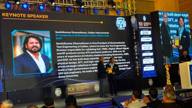
Caliber Interconnects demonstrated its renewed focus on semiconductors and technology innovation at the IEEE International Test Conference (ITC) India 2026 through a host of technically rich sessions including a keynote presentation, tutorial, IEEE paper presentations, poster sessions, industry display showcase and panel discussions. The keynote titled ‘From Silicon Complexity to AI Revolution – India’s Silicon Leap 2047′ was delivered by Senthilkumar Dhamodharan, Vice President – Testing, Caliber Interconnects. The keynote, presented on ‘From Silicon Complexity to AI Revolution – India’s Silicon Leap 2047′, by Senthilkumar Dhamodharan, Vice President – Testing, Caliber Interconnects elucidated India’s ascension to global semiconductor status and the influence of AI on next-generation chip technologies.
The keynote examined the transformative role of Artificial Intelligence in reshaping the global semiconductor industry amid increasing silicon complexity, heterogeneous integration and advanced packaging technologies. It outlined how AI is revolutionizing every stage of the semiconductor lifecycle—from intelligent chip design automation and predictive manufacturing to AI-driven Automated Test Equipment (ATE), digital twins and advanced signal integrity analysis—helping improve product quality, accelerate time-to-market and enhance manufacturing efficiency. As Global demand accelerates semiconductors have become the foundation of digital economies, powering applications ranging from AI and autonomous systems to telecommunications, healthcare and defence.
The presentation also highlighted India’s growing strategic importance in the global semiconductor value chain. Drawing on the momentum created by the India Semiconductor Mission, emerging fabrication and advanced packaging initiatives, and the country’s globally recognised semiconductor design talent, the keynote presented a compelling roadmap for India’s evolution into a global hub for semiconductor design, manufacturing, testing and innovation.
Emphasising the vision of Viksit Bharat 2047, the address called upon industry leaders, researchers, policymakers, academia and the IEEE community to strengthen collaboration, develop indigenous test engineering capabilities, embrace AI-enabled validation methodologies and build a resilient, globally competitive semiconductor ecosystem.
Beyond the keynote, Caliber demonstrated its technical leadership by presenting one tutorial, four IEEE technical papers, four poster presentations, participating in an Industry Showcase and contributing to a high-level panel discussion. The company’s presentations focused on emerging challenges and innovations in AI- driven semiconductor testing, Design for-Test (DFT), Automatic Test Pattern Generation (ATPG), MBIST/LBIST, silicon debug, reliability testing, advanced-node devices, chiplets and AI accelerators.
IEEE ITC India 2026 served as an important platform for fostering industry-academia collaboration, promoting AI and machine learning applications in semiconductor test automation, yield improvement and test cost optimisation, while encouraging knowledge exchange among professionals, researchers and students.
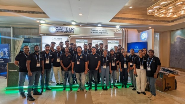
Caliber’s exhibition booth attracted visitors, including semiconductor industry professionals, researchers, academicians and IEEE Fellows. The booth welcomed representatives from leading global technology companies including Texas Instruments, AMD, Qualcomm, Synopsys, NVIDIA, Broadcom, Marvell, SanDisk, Google, Siemens, Infineon, Teradyne, Advantest and Tessolve, alongside faculty and researchers from premier institutions such as IIT Patna, IIIT Kottayam, VIT Vellore, the University of Stuttgart, PSG College of Technology and several other universities. The interactions generated meaningful technical discussions and opened new avenues for research collaboration and industry partnerships.
Commenting on the event, Senthilkumar Dhamodharan said, “The future of semiconductors will be shaped by the convergence of AI, advanced testing and collaborative innovation. India has a unique opportunity to lead this transformation by combining its design excellence with world-class manufacturing, testing capabilities and a strong innovation ecosystem. IEEE ITC India provides an excellent platform to collectively build this vision for Viksit Bharat 2047.”
Caliber Interconnect’s strong participation at IEEE ITC India 2026 reflects the company’s continued focus on driving innovation in semiconductor testing, advancing AI-enabled engineering solutions and contributing to India’s emergence as a trusted global semiconductor technology leader.
The post Caliber Interconnects Showcases AI-Powered Semiconductor Testing at IEEE ITC India 2026 appeared first on ELE Times.
Photon Design enables multi-junction VCSEL simulation for high-power applications
The security imperative for software-defined vehicles

The automotive industry has undergone a major transformation, shifting from traditional hardware-centric vehicles to software-defined vehicles (SDVs). Unlike conventional cars, SDVs continuously evolve through over-the-air (OTA) updates, unlocking new features, optimizing performance, and enhancing safety over time.
While this shift continues to enable greater connectivity, automation, and personalization, it also expands the cybersecurity threat landscape. As SDVs integrate with cloud systems, mobile apps, and AI-driven features, they become more vulnerable to cyberattacks. Ensuring robust security frameworks is critical to unlocking the full potential of SDVs while safeguarding user safety and data privacy.
What makes SDVs unique?At the heart of SDVs is a shift in computing architecture. Traditional vehicles relied on multiple fixed-function electronic control units, but as software complexity grows, automakers are shifting toward zonal architectures. By dividing vehicles into manageable zones powered by system-on-chips, manufacturers can streamline software updates, optimize performance, and future-proof vehicle systems against obsolescence.
However, this software-driven transformation also creates security challenges. The sheer scale of SDV software is unprecedented: Traditional vehicles already contain about 100 million lines of code, and as fully autonomous Level 5 driving emerges, this number is expected to surpass 1 billion lines. The growing attack surface demands a proactive cybersecurity strategy to prevent vulnerabilities from being exploited.
 Automakers need to implement a multilayered defense strategy that encompasses multiple security measures across the entire ecosystem to build a secure SDV ecosystem. (Source: Adobe Stock)
The expanding cybersecurity threat landscape
Automakers need to implement a multilayered defense strategy that encompasses multiple security measures across the entire ecosystem to build a secure SDV ecosystem. (Source: Adobe Stock)
The expanding cybersecurity threat landscape
Unlike their predecessors, SDVs are no longer isolated machines. Instead, they function as interconnected platforms, continuously exchanging data with cloud networks, IoT devices, and other vehicles. While this level of interconnectivity unlocks powerful capabilities, it also increases exposure to cyberthreats.
Without strong encryption and data protection measures, cloud-connected vehicles risk having sensitive driver information compromised. AI-powered personal assistants and autonomous-driving systems must be designed with robust privacy safeguards to prevent unauthorized tracking or manipulation.
Compounding the risk is the lack of standardized security frameworks across the industry. While standardization efforts are advancing, every automaker develops proprietary software and interfaces, leading to inconsistencies in security implementations. These inconsistencies create opportunities for cybercriminals to exploit fragmented security protocols. A single vulnerability in one system could serve as an entry point for attackers to gain access to critical vehicle functions, jeopardizing both data privacy and operational safety.
Supply chain risks also contribute to the security dilemma. Modern vehicles rely on third-party software and hardware providers, each of which may introduce vulnerabilities that adversaries can exploit.
Furthermore, SDVs must support a mix of legacy and cutting-edge systems, making it difficult to implement uniform security measures across all components. The absence of an industry-wide security standard exacerbates these risks, as automakers struggle to balance innovation with the need for strong protections.
This growing digital ecosystem extends beyond the vehicle itself. Automakers now maintain ongoing digital relationships with drivers through software-based subscriptions and AI-powered enhancements, often leveraging mobile apps for remote vehicle control. While these applications provide convenience, allowing users to start their cars, unlock doors, or adjust vehicle settings from anywhere, they also introduce critical security vulnerabilities.
If mobile apps are not properly secured with strong authentication and robust software protections, cybercriminals could exploit weaknesses to hijack these functions, potentially gaining control over vehicles or tracking driver locations in real time.
Mobile apps also store personally identifiable information, such as driver profiles, payment details, and vehicle usage data, making them attractive targets for cybercriminals. This further increases the need for stronger authentication protocols, end-to-end encryption, and strict compliance with privacy regulations such as GDPR and CCPA.
Real-world incidents have already demonstrated the dangers of inadequate security. Just last year, researchers uncovered vulnerabilities in Subaru’s Starlink system that allowed remote attackers to unlock and start millions of vehicles, track their locations, and access extensive driving histories. While Subaru quickly patched the flaw, the incident highlighted the urgent need for automakers to adopt more comprehensive cybersecurity frameworks.
Building a secure SDV ecosystemSecuring SDVs goes beyond simply implementing technical solutions. It requires fostering a robust security culture within organizations, using certified solutions, and relying on independent third-party assessments to ensure compliance with ever-evolving industry standards. A fragmented approach to security can leave dangerous gaps that attackers are quick to exploit.
Security must be integrated from the ground up, beginning at the chip and silicon IP level to prevent hardware-based exploits. Adopting a bottom-up security architecture ensures that every layer, whether it be firmware, software, network communications, or cloud services, remains protected against potential cyberthreats.
To build a truly secure SDV ecosystem, automakers must implement a multilayered defense strategy that encompasses multiple security measures across the entire ecosystem. This strategy starts with hardware-based security, which prevents tampering at the chip level, ensuring that foundational components remain secure. From there, AI-driven threat detection becomes essential, as it enables vehicles to continuously monitor and respond to emerging cyberthreats in real time.
Equally crucial is the establishment of a secure cloud infrastructure. This includes implementing encrypted data storage, strict access controls, and continuous monitoring to safeguard against cloud-targeted attacks. Additionally, OTA updates must be encrypted to ensure that software changes are secure and tamper-proof, thus protecting against potential supply chain attacks.
Finally, securing access to the vehicle itself is paramount. Strong authentication and identity management systems must be in place to ensure that only authorized individuals can interact with critical functions, such as unlocking doors or tracking the vehicle’s location.
Creating a secure SDV ecosystem is a collaborative effort among engineers, security teams, and end users. Automakers must cultivate a security-first culture, ensuring that cybersecurity awareness is ingrained at every level of development. Teams must be trained to anticipate, detect, and respond to threats proactively and effectively.
The road aheadSDVs represent a paradigm shift in the automotive industry, offering continuous improvements but also introducing security challenges. As AI, automation, and cloud connectivity become integral to modern mobility, cybersecurity will remain a priority for automakers.
Looking ahead, advancements such as quantum computing and the need for quantum-resistant cryptography will further reshape the cybersecurity landscape. To stay ahead of these developments, automakers must proactively strengthen security frameworks, embedding protection at every layer from silicon to software. By taking a proactive approach to cybersecurity, the industry can unlock the full potential of SDVs while ensuring safety, reliability, and trust in the vehicles of the future.
The post The security imperative for software-defined vehicles appeared first on EDN.
Blue’s original Snowball: A multi-capsule sonic catch-all

Two capsules. Two consequent pickup-pattern options. Three pickup-setting options. What’s not to like (aside, maybe, from the cosmetics)?
In November 2022, EDN published my introductory treatise on standalone microphones. At the time, I mentioned that two examples of the USB-interface Blue (now Logitech) Snowball microphone were (and had for some time been…since late 2007, my email archive informs me!) in my possession, one of them destined for teardown.

I subsequently also acquired two Snowball iCE mics, one of which I took apart, wrote about and EDN published back in May. The Snowball iCE, released a decade (2015) after its original Snowball sibling (2005), is a lower-cost (and -priced) single-capsule condenser variant of the original design, therefore supporting only a cardioid pickup pattern.

I’ve finally gotten around to actualizing the several-year-back initial aspiration to disassemble the original Snowball, with the fruits of my labors detailed today. As usual, I’ll start out with a set of outer box shots, in each case (along with other photos to follow) accompanied by a 0.75″ (19.1 mm) diameter U.S. penny for size comparison purposes.


Brace yourselves: here come the most existing ones of the lot (not).


With that riveting visual intro out of the way, let’s see what’s within. Accessories include a USB-A to USB-B cable, akin to those commonly used with printers, this time microphone-destined.

And a three-legged stand, conceptually similar to—albeit this time more sturdily constructed than—the one included with its more economical Snowball iCE cohort.

Of course, there’s also our stand-disconnected dissection victim. Front.

Left side.

Back: visible is the USB-B male connector, handling both power (input) and digital audio data (output), and the three-position switch alluded to in the subhead. The switch settings reference the following functional options and other implementation nuances:
- Position 1
- Setting: Cardioid (capsule)
- Applications: speech, vocals, and podcasting
- Picks up sound from the front, ideal for podcasting, game streaming, or recording vocals and instruments
- Position 2
- Setting: Cardioid (capsule) with -10dB pad
- Applications: live music and loud sound sources
- Reduces mic sensitivity, so loud instruments or vocalists come in crystal clear and distortion free
- Position 3
- Setting: Omnidirectional (capsule)
- Applications: conferences, interviews, and environmental recordings
- Picks up sound all around the mic, perfect for conference calls or recording a group of musicians
Onward. Right side.

Top, showcasing the pointed-forward power LED.

And bottom, with the vertical-swivel (45° tilt up and down) screw-hole connection to the earlier-seen stand.

Now to get inside the mic itself. The procedure is exactly the same as for the Snowball iCE, which I’ve already textually and photographically documented in exhaustive detail back in May. So, I’ll back-reference you for the specifics versus doing a repeat performance. The only variance is that the shiny silver ring around the circumference is metal (with an adhesive backing) this time, versus just a sticker (another cost-reduction move that Blue-then-Logitech apparently made with the Snowball iCE).

Remove the black foam sheet from the front half.

And as before, you’ll see the connection to the power LED.

Now for the much more interesting (at least to me) back half.

Completely remove the four screws that originally held the two halves together:


And the guts detach from the back-half housing straightaway.


There’s a hefty metal plate in-between the multi-capsule assembly and the PCB.

See those three screw heads? You know what comes next.


Back in May, I mentioned a competitor-sourced controversy regarding just how many condenser pickup capsules the Snowball contained. But in revisiting the referenced October 2023 prior-coverage source, I realized that I hadn’t yet provided the associated visual evidence. The competitor was another USB-interface dual-pattern mic I’d disassembled, JLab’s Talk GO. And here’s the belated comparative graphic, presumably JLab-sourced, although published at the product page of a retail channel partner, Woot (where I’d bought mine).

I don’t know about you, but this sure looks like two condenser capsules inside the Snowball to me. Agree?


Now for the PCB, beginning with the comparatively boring front side that normally nestles up against the metal plate (but doesn’t actually touch it, which would short out those solder points, thanks to thin white plastic spacers that keep them apart).

Here’s the more intriguing, or at minimum, more populated backside:

You’ll see in a minute where the two grey multi-wire harnesses at top and left end up. You’ve already seen where the yellow-and-white one also at the top goes (the front/top power LED), as well as the two red-and-black ones (the two condenser pickup capsules). But what about the ICs in the middle? I thought you’d never ask.

The Snowball iCE’s dominant audio ADC-plus-USB interface device was C-Media Electronics’ CM6327A. This time it’s Micronas’ UAC 3556B, first publicly discussed more than a quarter century ago (!!!) and curiously positioned as “enabling Voice over Internet Protocol (VoIP) functionality, integrating an additional audio channel directly into existing USB keyboard architectures” (???).
It includes a two-channel ADC, although per the datasheet (PDF), only one of the two channels can optionally act as either an (electret) microphone or line input, with the other only supporting line levels. Presumably, the UAC 3556B also implements back panel switch position #2’s input attenuation function. The IC’s integrated DAC is seemingly unused.
Speaking of the back panel switch, and in closing, there’s this last shot.

Showing, as previously promised and after more black foam removal, where those two grey multi-wire harnesses end up at their other ends. And with that, I’ll wrap up for today. Share your thoughts in the comments, please!
—Brian Dipert is the associate editor, as well as a contributing editor, at EDN.
Related Content
- Microphones: An abundance of options for capturing tones
- The Blue (now Logitech) Snowball iCE: This mic sounds nice
- Checking out a USB microphone
- Microphones: On-PCB options for catching tones
- Disassembling an in-line microphone preamp
The post Blue’s original Snowball: A multi-capsule sonic catch-all appeared first on EDN.
Billion Electric, JK Cement Partner to Deploy 150 Heavy-Duty Electric Trucks for Green Freight
Billion Electric Mobility (BillionE) has partnered with JK Cement to deploy 150 heavy-duty electric trucks across Karnataka, Maharashtra and Goa, making one of the region’s largest deployments of electric trucks for cement logistic. The collaboration began with an initial fleet of 20 electric trucks from JK Cement’s Muddapur plant in Karnataka, with the remaining vehicles planned to be introduced in phases. The partnership represents a significant step in the adoption of battery-electric vehicle for heavy duty transportation. The truck is expected to be deployed in phases by March 2027, according to reports.
This latest deployment by JK Cement is one of the largest deployments of electric trucks in the cement sector in India. The project will help the company gain practical experience in operating heavy-duty electric trucks on high-volume transport routes and in challenging conditions. It will also demonstrate the potential of electric trucks for B2B logistics and commercial freight operations.
The initial fleet will feature Montra Electric’s Rhino 5538, a 55-tonne electric truck. The model will be available in both tipper and tractor-trailer versions, with JK Cement initially deploying the tractor-trailer variant. The truck will be offered in a 4×2 configuration and powered by a 280-kW electric motor and a 282-kWh LFP battery pack. Depending on the variant and operating conditions, it is claimed to offer a range of 198 km or 169 km. The battery can be charged from 20% to 100% in approximately one hour.
The phased deployment by BillionE and JK Cement aims to show that electric trucks can support regular, real-world freight operations at scale, rather than being limited to small pilot projects. By combining high-capacity electric trucks, fast charging, and smart route planning, the project could provide a model for the logistics industry to move towards zero-emission freight transport.
The post Billion Electric, JK Cement Partner to Deploy 150 Heavy-Duty Electric Trucks for Green Freight appeared first on ELE Times.
India Moves Ahead with Netra Mk II: Six Airbus A321s to Become Advanced Airborne Surveillance Platforms
Now, India is about to move a further step ahead in enhancing its airborne surveillance and monitoring with the development of Airborne Early Warning and Control (AEW&C) Mk II or Netra Mk II. Under the programme, six Airbus A321 aircraft will be converted into sophisticated airborne surveillance aircraft. Reports suggest that DRDO has inked a contract with the aviation giants to get the jets converted as advanced Airborne Early Warning and Control aircraft, as per the Defence Analysis Wing of India’s Defence Ministry.
These new aircraft are supposed to carry advanced electronic warfare systems which are also capable of detecting and tracking aerial targets at high altitudes and from large distances. Equipped with highly capable radars and state-of-the-art electronic sensors, such platforms allow commanders to expand their real-time battlefield awareness and to effectively command coordinated counter-attack actions.
Electronic Age of warfare: “With the production of this aircraft, we would reduce our dependence on imported advanced electronics for such applications and achieve indigenisation”. Said by Mr R.N. Murali, Director. R&D facility, India. With the development of Netra Mark II, electronics will play just as important a role as our traditional weapons. Improved radars, data link, secure radio, processing capability & C2 system. The technology has to be a force for our country.
The programme is poised to enhance India’s indigenous air surveillance capability, enabling it to quickly respond to developing situations, and improving sky surveillance.
The post India Moves Ahead with Netra Mk II: Six Airbus A321s to Become Advanced Airborne Surveillance Platforms appeared first on ELE Times.
India Strengthens Counter-Drone Defence with AI, Radar and Electronic Warfare
India is rapidly developing solutions for this threat of drone swarms and unmanned aerial systems that are proving to be a major problem for troops on modern battlefields. Its own drone counter system now incorporates radar and electro-optical and infrared sensors together with radio frequency detection and electronic warfare systems.
Through this technology a defence force should be able to not just detect and identify a drone, but also monitor it and determine an appropriate response. For example, radar can detect drones as soon as they enter the operational area, then other better sensors can be used to corroborate a possible threat. Defensive electronic warfare devices may also be able to jam the drone’s navigation or communication system.
AI is predicted to have even a greater responsibility and help humans understand what they detect much faster, especially because AI processes sensor data. This includes detecting whether it is a bird or an insect etc. And identifying which is threatening amongst several targets, etc.
As drone technology becomes a cheaper alternative for even those with limited budgets, it’s telling how much New Delhi’s priorities to tech have turned to ‘state-of-the-art counter-drone electronics’ which, after all, seems like it could be another front on which to engage any future enemy; after all, the ‘next-gen battlefield might be determined not so much by firepower, but by those capable of finding targets the quickest, processing information the best, and fighting the smartest.
The post India Strengthens Counter-Drone Defence with AI, Radar and Electronic Warfare appeared first on ELE Times.
Delhi EV Policy 2026: New Subsidy Portal Aims to Accelerate Electric Mobility with ₹15,000- Crore Budget
New EV Policy 2026 Announced BY THE DELHI GOVERNMENT FOR THE NATIONAL CAPITAL Delhi’s new Electric Vehicle (EV) Policy 2026 is set for a radical change for its citizens who would be encouraged to switch to cleaner ways of transport, predominantly through the use of Battery Electric vehicles (BEVs) in the national capital. With a proposed outlay of INR 15,000 crores across a period of 4 years, the policy approved by the Delhi Cabinet and implemented by July 1, 2026, promises to further drive the agenda for zero- emission-based commuting, keeping in mind the city’s alarming and growing problem of air pollution.
To ensure a smooth subsidy process, another major initiative that comes with this updated policy is the introduction of the Delhi EV Subsidy Portal. The portal allows successful EV buyers to apply online for purchase and scrappage incentives, monitor application status and directly receive subsidized benefits through the Direct Benefit Transfer (DBT) system. The portal was introduced to make the subsidy process more transparent, accessible, and efficient for EV buyers.
This new policy marks a substantial boost in Delhi’s initiative to promote electric mobility. The state government is set to spend Rs 15,000 crore under the scope of the policy that will be effective until March 31, 2030. Much of the anticipated investment is set to support EV incentives, infrastructure charging support and other schemes geared towards creating a comprehensive EV ecosystem.
Delhi’s new INR 15,000-crore EV Policy 2026 represents one of the most ambitious state-level efforts in India to accelerate the transition towards electric mobility. By combining purchase subsidies, scrappage incentives, tax exemptions, charging infrastructure expansion, technology-based eligibility requirements, and phased registration measures, the policy seeks to create a comprehensive framework for increasing EV adoption.
The post Delhi EV Policy 2026: New Subsidy Portal Aims to Accelerate Electric Mobility with ₹15,000- Crore Budget appeared first on ELE Times.
India Approves Two Electronics Manufacturing Clusters in Tamil Nadu to Strengthen Domestic Electronics Ecosystem
Govt Approves Establishment of 2 New Electronics Manufacturing Clusters in Tamil Nadu, India to Boost Electronic Manufacturing Ecosystem. A further boost to the indigenous electronics manufacturing ecosystem has been given today. Government of India approves the setting up of two new Electronics Manufacturing Clusters (EMCs) in Tamil Nadu. A total outlay of Rs 1012 crore will be put into developing these EMCs, which will be constructed at Manallur and Pillapaikkam, creating a push towards industrial infrastructure development and attracting electronics manufacturers.
Union Minister for Electronics and Information Technology Ashwini Vaishnaw announced the approval through a written reply in the Lok Sabha on July 22, 2026. Under the two projects, the two industrial locations to be created will be spread over 850 acres, and will house units operating in diverse segments of the value chain of electronics companies.
Tamil Nadu State Electronics Manufacturing centres are one of the major centres in India in terms of electronics investment. With such investments, the state emerged as top hub in terms of investment and production in electronics manufacturing especially mobile phone manufacturing, assembly and automotive electronics manufacturing, and their supporting industrial sector. Manallur and Pillapaikkam EMC’s, after approval by GOI, might consolidate the existing manufacturing base while enabling the set up and expansion of new companies by Indian as well as foreign companies.
The approval of the Manallur and Pillapaikkam Electronics Manufacturing Clusters represents another important development in India’s effort to strengthen domestic electronics production. With a combined project cost of approximately ₹1,012 crore and a total area of more than 850 acres, the two clusters will add new manufacturing infrastructure to Tamil Nadu’s already significant electronics ecosystem.
The post India Approves Two Electronics Manufacturing Clusters in Tamil Nadu to Strengthen Domestic Electronics Ecosystem appeared first on ELE Times.
V-GaN Tech Hub opens Test and Characterization Facility to accelerate microelectronics from lab to fab
Power electronics market to grow at 10% CAGR from US$25.5bn to US$65.2bn by 2036
First experimental demonstration of S-band large-signal performance for GaN HBTs
StraitsMicro to Unveil India’s Sovereign Surveillance SoC in Exclusive Pre-Silicon Demonstration
StraitsMicro, a Singapore-based deep-tech semiconductor product development and solutions company, is unveiling Visora, its sovereign Camera System-on-Chip (SoC) family, at an exclusive pre-silicon demonstration. Visora serves as the core processing engine for CCTV cameras and is designed as a secure, indigenous silicon alternative, addressing the gap created by the Government of India’s restriction on Chinese SoCs in surveillance hardware. Positioned as India’s sovereign surveillance SoC family, Visora is built for government, defence, smart-city, and critical-infrastructure use across India and global markets.
The company is taking its proof-of-concept to market through a series of three showcase touchpoints, supported by partners Proxelera (Bengaluru-based design partner), Aqtronics (distributor), with the India-Singapore semiconductor partnership as a supporting narrative.
Commenting on the demonstration, Mr. Pankaj Sharma, Founder & CEO, StraitsMicro, said, “Today marks the successful pre silicon validation of our indigenous CCTV Camera Edge AI SoC architecture. This reflects our commitment to developing trusted, secure and intelligent semiconductor solutions for surveillance and other applications for the Indian and global market. Our aim is to build a globally competitive semiconductor company leveraging India’s talent and strengths in design and Singapore’s capabilities and prowess in fabrication, manufacturing, quality and reliability engineering for semiconductors. With India as a major innovation and development hub duly complemented by Singapore with a robust semiconductor ecosystem, we look forward to working with government, industry, customers and partners to build relevant and trusted semiconductor solutions. This is only the beginning of our product and solutions roadmap. We welcome strategic partners and customers to join us on this exciting journey.”
The event featured a live FPGA-based Camera SoC demonstration, showcasing proposed AI features, security architecture, and performance. The Visora roadmap spans three products for CCTV and one product for Network Video Recorder (NVR). The entry-level Visora Edge supports video up to 5MP at 30fps for residential cameras, retail security, small and medium businesses and other cost-sensitive IP-camera applications. The mid-range Visora Secure supports up to 8MP at 30fps, an integrated AI accelerator and advanced low-light imaging for commercial surveillance, industrial applications, smart cities, traffic monitoring, railways and metros. The high-end Visora Pro scales to 4K at up to 120fps and can support up to eight cameras for defence, border security, safe-city projects, airports and other critical infrastructure. The Visora Network SoC for NVRs completes StraitsMicro’s trusted surveillance semiconductor platform by extending hardware-rooted security from the camera to the network, ensuring secure video processing, storage, and transmission while mitigating cyber threats and data leakage across the surveillance ecosystem.
Across the family, the proposed architecture combines an ultra-low-power multicore 64-bit CPU with hardware-accelerated AI, low-power DDR5, and H.265 video encoding, delivering very high compression. The frame-to-stream imaging pipeline incorporates multi-exposure HDR, motion-compensated 3D noise reduction, wide-angle and fisheye distortion correction, and on-chip lossless buffer compression that can reduce memory-bandwidth demand. Depending on the model, edge-AI functions range from motion and human detection to crowd analytics, facial recognition, behaviour analytics and advanced edge inference.
Mr. KT Chan, Director – Services & Partners, StraitsMicro, added, “Having spent three decades in the semiconductor industry, I believe trusted semiconductor technologies will play a critical role in the future of secure AI semiconductor solutions. StraitsMicro combines extensive experience, leadership, strong technical skills and capabilities, an innovative product development approach and international partnerships with worldwide reach to create semiconductor products and solutions in India with global relevance. Our goal is not only to develop world class semiconductor solutions but also to contribute to a trusted and resilient semiconductor ecosystem. We thank all our customers and partners for their support and look forward to creating lasting value together.”
StraitsMicro’s approach centers on fostering the electronics and semiconductor ecosystem through the establishment of a Semiconductor Development Hub for indigenous new products through co-creation; and providing value addition to domestic fabless semiconductor companies to help them build indigenous products, a holistic approach to developing the electronics and semiconductor ecosystem, spanning both the domestic and global markets.
The post StraitsMicro to Unveil India’s Sovereign Surveillance SoC in Exclusive Pre-Silicon Demonstration appeared first on ELE Times.
Kia Expands India’s EV Portfolio with New Syros Electric SUV
Kia India has added the Kia Syros EV, a compact electric SUV designed for India, to its EV line-up. The car carries a base price of ₹13.49 lakh (ex-showroom) and boasts a maximum ARAI-certified range of 526 km, as Kia strengthens its portfolio in India’s EV landscape. Deliveries of the Kia Syros EV will begin from July 30, 2026, across the brand’s dealerships.
The introduction of this vehicle marks a critical development in Kia’s objective to accelerate the pace of electrification and bring it into the reach of more and more Indian buyers. The Syros EV would be a compact SUV that integrates driving range, connectivity, driver-assistance technology, and practical urban dimensions as a complete package, derived from the existing Syros body style but features EV-specific modifications, a different front-end styling, an external charging port and a front trunk.
A key highlight of the vehicle is its battery and range capability. The larger 51.4-kWh battery pack provides an ARAI MIDC-certified range of up to 526 km, placing the Syros EV among the long-range options in its segment. Kia also offers two battery options, allowing customers to choose between different combinations of range, performance, and price. The company claims that the vehicle can be charged from 10% to 80% in approximately 39 minutes using a 100-kW DC fast charger under standard test conditions.
Launched at a time when there is already high competition in Indian electric subcompact SUV market. SyrosEV will compete with leading and well-established electric contenders in India such as Tata Motors & Mahindra. Combined with its small footprint as well as 500 km range claims, the car gets packed features and ownership options to stand out from the competition in the segment. As buyers are most anxious about charging options, range, battery warranty, & driving cost.
The post Kia Expands India’s EV Portfolio with New Syros Electric SUV appeared first on ELE Times.
Micro power generators: Turning everyday flows into energy

Engineers are redefining energy by looking not at massive grids but at the overlooked flows around us. Rain gutter generators that channel storm runoff, tap-mounted turbines spinning with household water, and balcony-scale wind turbines catching urban breezes prove that power can be harvested wherever motion exists.
These micro power generators embody the spirit of engineering empowerment, transforming ordinary infrastructure into sustainable energy assets. By designing systems that thrive on the smallest currents, engineers are not just solving technical challenges; they are enabling a future where autonomy, resilience, and sustainability are built into the everyday fabric of life.
Harnessing gravity: Micro hydro power
You don’t need a colossal dam to tap into hydroelectricity—gravity and flowing water are enough. Whenever water moves downward, whether from a rooftop gutter or a household faucet, it carries kinetic energy that can be captured and converted into usable current.
Micro hydro systems thrive on small vertical drops, known as “head,” which create surprising pressure even in everyday settings. A rain gutter turbine, often built around a miniature Pelton wheel, can be placed at the base of a downspout so that rainfall from a two-story home delivers enough head to charge an outdoor battery bank, turning stormwater into renewable energy storage.
Faucet hydros, on the other hand, are pocket-sized turbines that screw directly onto sinks or showerheads, producing between 5-V and 12-V DC—the perfect range for powering smart water temperature displays, LED bathroom lighting, or other low-voltage gadgets. Together, these simple setups prove that even the smallest streams of water can be harnessed to generate clean electricity, making hydro power accessible at the scale of everyday living.

Figure 1 Micro-hydroelectric power generators convert kinetic energy from small water streams into sustainable electrical power. Source: Author
Catching the breeze: Urban wind
Just as falling water can be harnessed for energy, moving air offers another everyday source of clean electricity. Standard windmills are massive, but compact vertical axis wind turbines (VAWTs) are reshaping the landscape for residential use. Unlike the towering three-blade giants on hillsides, these turbines resemble kinetic sculptures, blending into urban settings while quietly generating power.
Their design makes them safer for birds, more tolerant of turbulent wind bouncing off fences or house walls, and ideal for small spaces where airflow is unpredictable. With the ability to charge 12-V batteries, they provide reliable energy for garden sheds, security cameras, or other low-voltage systems, proving that even the breezes swirling through neighborhoods can be transformed into practical power.

Figure 2 Mini wind turbines harvest kinetic energy from turbulent urban breezes to provide localized renewable power. Source: Author
Harvesting the invisible: RF and Wi-Fi
If water and wind can be turned into electricity, why not the invisible waves that surround us every day? It may sound like science fiction, but it’s pure physics: electromagnetic energy from routers, cell towers, and radio stations constantly fills the air. RF energy harvesters capture this ambient power using a specialized antenna called a rectenna, which converts radio frequency signals into direct current. The output is small—usually measured in microwatts (𝜇𝑊)—but it’s enough to sustain ultra-low-power devices.
Imagine a moisture sensor in your garden that never needs a battery because it feeds on the Wi-Fi signal leaking from your window, or a network of “batteryless” sensors quietly monitoring conditions without ever needing replacement. By tapping into the invisible spectrum, RF harvesting extends the idea of micro power generation into the realm of everyday signals, proving that even the unseen can be harnessed for sustainable living.

Figure 3. The AEM30940 PMIC manages energy extraction from piezoelectric, micro-turbine, or high-frequency RF sources. It simultaneously charges a storage element while providing two independently regulated output voltages to power system components. Source: e-peas
Power from difference: Thermal energy
Just as water and wind can be harnessed for electricity, temperature itself can drive power generation through the Seebeck Effect. When one side of a material is hot and the other is cold, electrons begin to move, creating a voltage difference that can be captured as usable current.
This principle is already at work in stove-top generators found in many off-grid cabins, where a thermoelectric fan sits with its base on a hot wood stove and its top cooled by surrounding air. The temperature gradient produces enough electricity to spin the fan, circulating warmth throughout the room without external wiring.
On a smaller scale, wearable thermoelectric generators (TEGs) are emerging as a way to harvest body heat, powering fitness trackers and other low-power devices directly from the warmth of your skin. By turning everyday temperature differences into electricity, thermal energy harvesting extends the reach of micro power generation into both rustic cabins and modern wearables, proving that even the contrast between hot and cold can be transformed into sustainable current.

Figure 4 Stove-top thermoelectric generators convert waste heat into usable electricity. Source: TEG
Sunbeams to volts: The “magic” of micro-solar
At its heart, solar is the only micro-generator that feels like literal magic: it has zero moving parts, no loud turbines, and it runs on nothing but daylight. The fundamental “trick” is simply catching photons to knock electrons loose, creating a silent flow of power. Today, this technology is defined by “energy independence in a box,” where ultra-portable power stations—utilizing long-lasting LiFePO4 batteries and AI-driven energy management—allow anyone to build a personal power grid in minutes.
We’ve come a long way from the flimsy calculators of the 90s. From high-efficiency bifacial panels that harvest light from both sides to the emergence of perovskite-silicon tandem cells that pack 25% more power into the same small footprint, solar micro-generators provide a fuel-free alternative to traditional engines.
Whether it’s a balcony-mounted micro-inverter system or a foldable camping mat, solar is no longer just a “green” alternative; it’s the most reliable, scalable tool for decentralized power in our modern world. It’s basically like having a tiny, silent utility company that you can carry in your backpack.

Figure 5 N-type TOPCon dual-glass bifacial solar panels maximize energy harvesting by capturing incident sunlight on the front surface while simultaneously absorbing reflected light from the rear. Source: Author
Power of a pulse: Stepping into piezo power
While solar catches light, piezoelectric generators catch movement. The fundamental principle is almost toy-like in its simplicity: certain materials, like specialized ceramics or crystals, generate an electric spark when you squeeze or deform them.
In the world of micro-generation, this means turning everyday “wasted” energy—like the thud of a footstep, the vibration of a passing train, or even the pulse of a finger on a keyboard—into usable volts. Today’s technology has miniaturized this into “energy harvesting skin” and thin-film polymers that can be embedded into everything from smart sneakers to bridge supports.
Unlike solar, which needs the sun, or wind, which needs a breeze, piezo power only needs action. It’s the ultimate “hidden” generator, silently sipping energy from the vibrations of the world around us. While a single “squeeze” might only power a tiny sensor or a wireless signal, scaling this tech into “smart floors” or wearable fabrics is turning the human body and our infrastructure into a living, breathing power plant. It’s the fundamentals of physics turned into a literal “walk in the park” for renewable energy.

Figure 6 Cantilever piezoelectric harvesters convert mechanical strain from bending and vibrations into usable electrical energy. Source: Smart Material
Designing lean systems for ultra-low power
For engineers and makers, the frontier of micro power isn’t just about capturing energy; it’s about designing lean, ultra-low-power systems that thrive on the tiniest trickles of current. By leveraging efficient voltage regulators, sleep-mode microcontrollers, and energy-aware communication protocols, you can stretch microwatts into meaningful work.
Smart design tricks—like duty-cycling sensors, harvesting capacitors for short bursts, and matching generator output to the load—transform fragile prototypes into reliable systems. Today’s ecosystem of modular rectennas, plug-and-play thermoelectric modules, and ultra-low-power ICs makes experimentation easier than ever, giving designers the tools to tailor micro power generators for domains ranging from smart homes to wearables.
Power your world with micro generators
Today’s maker landscape is rich with possibilities: micro hydro turbines, mini vertical-axis wind kits, piezo energy harvesters, and even RF harvesting modules are widely available online, often bundled as DIY systems that simplify setup for hobbyists. Many components—Pelton wheels, turbine housings, and airflow vanes—can be 3D-printed from open-source designs, making customization affordable and accessible.
Dedicated ICs such as ultra-low-power boost converters, energy harvesting PMICs, and rectifier-regulator modules are designed to stabilize and store trickle currents, while plug-and-play thermoelectric generators extend experimentation into thermal domains. With kits, printable parts, and specialized electronics at hand, building micro power generators across water, wind, signal, heat, light, and vibration/impact sources has become a practical weekend project rather than a distant engineering challenge.
The possibilities are here and the tools are ready—so why wait? Shock your imagination, spark your designs, and start building micro power generators that turn everyday forces into lasting energy solutions.
 T. K. Hareendran is a self-taught electronics enthusiast with a strong passion for innovative circuit design and hands-on technology. He develops both experimental and practical electronic projects, documenting and sharing his work to support fellow tinkerers and learners. Beyond the workbench, he dedicates time to technical writing and hardware evaluations to contribute meaningfully to the maker community.
Related Content
- Micro Hydro Generator
- Energy Harvesting Block Diagram
- Micro-Harvesting Will Not Power Our Planet
- What’s Happening in the World of Micro-Energy Harvesting?
- Platform design for testing vibration to electrical power generators
The post Micro power generators: Turning everyday flows into energy appeared first on EDN.
🏠 Про поселення на 2026/2027 навчальний рік

🔴 Відкриття першої хвилі реєстрації на надання місця в гуртожитку на 2026/2027 н.р. Місце в гуртожитку надається студентам та вступникам, які не зареєстровані у м. Києві.
Сторінки



