
Feed aggregator
I made my own open-source FPGA board.
 | I wanted to get started with FPGAs by making my own development board, and thus I made Arctyx Nano! https://github.com/Keyaan-07/Arctyx-Nano - everything is open-sourced under MIT License! Arctyx Nano is a low-cost, open source FPGA development board carrying the ICE40-UP5K FPGA from lattice along with the RP2350A in a raspberry pi pico form factor. It consists of 6 LEDs and one RGB LED. All the pins on both the ICs are used in one way or another. I am currently using APIO open-source toolchain to verify, simulate and build projects and to upload using APIO, i have to figure it out. This is my first FPGA PCB and i would love feedback on my design! This board was created as a project for hackclub blueprint, check it out!! [link] [comments] |
Small pcb pile
 | submitted by /u/goldfish_in_the_wall [link] [comments] |
The insides of a phone in a dorm room in Poland
 | submitted by /u/GRAPHENE9932 [link] [comments] |
High-voltage SiC MOSFETs power critical energy systems

Navitas is now sampling 2.3-kV and 3.3-kV SiC MOSFETs in power-module, discrete, and known-good-die (KGD) formats. Leveraging fourth-generation GeneSiC Trench-Assisted Planar (TAP) technology, these ultra-high-voltage devices offer improved reliability and performance for mission-critical energy-infrastructure applications.

According to Navitas, the TAP architecture uses a multistep electric-field management profile that significantly reduces voltage stress and improves blocking performance compared with trench and conventional planar SiC MOSFETs. In addition to increased long-term reliability and avalanche robustness, TAP incorporates an optimized source contact that enables higher cell-pitch density and improved current spreading. Together, these advances deliver better switching figures of merit and lower on-resistance at elevated temperatures.
Packaging options include the SiCPAK G+ power module, which uses epoxy-resin potting to deliver more than a 60% improvement in power-cycling lifetime and over a 10% improvement in thermal-shock reliability compared with similar silicone-gel–potted designs. Discrete SiC MOSFETs are offered in TO-247 and TO-263-7 packages, while KGD products provide system manufacturers with greater flexibility for custom SiC power-module development. AEC-Plus–grade SiC devices are qualified to standards that exceed conventional AEC-Q101 and JEDEC requirements.
To request samples of the ultra-high-voltage SiC MOSFETs, contact Navitas at info@navitassemi.com.
The post High-voltage SiC MOSFETs power critical energy systems appeared first on EDN.
Thermistors suppress inrush currents

S series NTC thermistors from TDK Electronics handle steady-state currents up to 35 A and absorb energy up to 750 J. They enable reliable inrush current suppression in switch-mode power supplies, frequency converters, photovoltaic inverters, UPS systems, and soft-start motors.

The S series includes two leaded variants—the S30 and S36—with disk diameters of 30 mm and 36 mm, respectively. The S30 features 7.5-mm lead spacing and a maximum power handling of 19 W, while the larger S36 has 19-mm lead spacing and extends power handling to 25 W. Both variants are rated for a wide climatic category of 55/170/21 in accordance with IEC 60068-1 requirements.
The S30 (ordering code B57130S0M000) and S36 (B57136S0M100) families cover basis resistance values of 2 Ω to 15 Ω and 2 Ω to 20 Ω, respectively. They support continuous currents ranging from 12 A to 25 A (S30) and 10 A to 35 A (S36). Permissible capacitances can reach up to 13,050 µF at 240 VAC (see datasheet for details). The table below summarizes the key electrical characteristics of the S30 and S36 variants.

To access the datasheets for the S30 series and S36 series, click here.
The post Thermistors suppress inrush currents appeared first on EDN.
Compact 1.25-kV MLCCs ensure stability

Murata has begun mass production of 1.25‑kV multilayer ceramic capacitors (MLCCs) with a capacitance of 15 nF in a 1210-size (3.2×2.5 mm) package. These MLCCs use a Class 1 ceramic dielectric (C0G, also known as NP0), making them a strong choice for onboard chargers in electric vehicles and power supply circuits in high-performance consumer devices.

Leveraging Murata’s ceramic and electrode materials, along with thin-layer molding and precision stacking technologies, these chip capacitors are optimized for the latest SiC MOSFETs. Thanks to the inherent advantages of C0G per EIA standards—low loss and stable capacitance across a temperature range of -55°C to +125°C—they are suitable for both resonant and snubber circuits.
For added design flexibility, 1.25‑kV MLCCs in the 1210 package are also available in capacitances from 4.7 nF to 12 nF. All of the new devices, including the 15‑nF chip, are offered with tolerances of ±1%, ±2%, and ±5%.
Datasheets for the new high-voltage MLCCs in the 1210 package can be accessed here.
The post Compact 1.25-kV MLCCs ensure stability appeared first on EDN.
Enhanced hybrid caps handle increased ripple current

Taiyo Yuden has launched the HVX(-J) and HTX(-J) series of conductive polymer hybrid aluminum electrolytic capacitors. These updated models offer a higher rated ripple current and a lower profile than previous HVX and HTX capacitors. They also meet the AEC-Q200 standard, ensuring reliability for automotive applications.

With increasing current demands in automotive power sources, there is growing need for hybrid capacitors that combine higher ripple current ratings, compact profiles, and a variety of sizes. The HVX(-J) and HTX(-J) series address this need, offering 36 different types. For example, the RAHTX331M1TFH0002JX achieves 3400 mA RMS at 135 °C—a 70% increase over the previous model’s 2000 mA RMS at the same temperature. Devices in the series are available in five package sizes, ranging from 8 mm in diameter and 10 mm in height to 12.5 mm in diameter and 13.5 mm in height.
The new hybrid capacitors offer rated voltages of 25 VDC to 63 VDC, capacitance values from 47 µF to 1000 µF, and high rated ripple currents at 135°C ranging from 2200 mA RMS to 4000 mA RMS. These performance characteristics make them well suited for noise suppression and power smoothing in automotive power-supply circuits, including control systems such as electric power steering and safety-critical applications like ADAS.
More information on the HVX(-J) and HTX(-J) series can be found here.
The post Enhanced hybrid caps handle increased ripple current appeared first on EDN.
Chip antennas boost Wi-Fi and UWB signal integrity

Three chip antennas from Taoglas—the ILA.257, ILA.68, and ILA.89—provide Wi-Fi 6/7, ultra-wideband (UWB), and ISM connectivity. Manufactured using a low-temperature co-fired ceramic (LTCC) process, the antennas deliver high radiation efficiency and frequency stability in ultra-compact packages. According to Taoglas, they also require a smaller keep-out area than competing antennas.

The ILA.257 is a 3.2×1.6×0.5-mm antenna for Wi-Fi 6/7, providing tri-band coverage across 2.4 GHz, 5.8 GHz, and 7.125 GHz with strong radiation efficiency and stable signal integrity. Its small footprint and minimal keep-out area make it well-suited for wearables, portable electronics, and industrial IoT devices.
Engineered for UWB operation from 6 GHz to 8.5 GHz, the ILA.68 3.2×1.6×1.1-mm antenna delivers a stable omnidirectional radiation pattern with consistent repeatability and low insertion loss. It supports applications such as indoor positioning, access control, and short-range radar in space-constrained IoT and automotive systems.
Designed for the 868-MHz and 915-MHz ISM bands, the ILA.89 supports global LPWAN and LoRa deployments with up to 47.9% radiation efficiency and 0.56 dBi peak gain. Its 4.0×12.0×1.6-mm footprint, simple layout, and regional variants help reduce design complexity and speed time-to-market for small IoT devices.
The ILA.257, ILA.68, and ILA.89 antennas are now available from Taoglas and its authorized distributors.
The post Chip antennas boost Wi-Fi and UWB signal integrity appeared first on EDN.
Handheld enclosures add integrated cable glands

OKW now offers CONNECT fast-assembly handheld plastic enclosures with optional integrated cable glands, making it easier to install power and data cables.
Cost-effective CONNECT is ideal for network technology, building services, safety engineering, IoT/IIoT, medical devices, analytical instruments, data loggers, detectors, sensors, test and measurement.
 (Source: OKW Enclosures Inc.)
CONNECT’s two case shells snap together for fast and easy assembly: no screws are required. This offers the choice of two ‘fronts’: one shell is convex – perfect for LEDs – while the other is flat and recessed for a compact display or membrane keypad. Inside the flat shell there are mounting pillars for PCBs and components.
CONNECT enclosures feature open apertures at each end. For these, design engineers can specify a combination of ASA+PC blank end panels and soft-touch TPE cable glands with integrated strain relief. Cable diameters from 0.134“ to 0.232“ are accommodated. The two long sides provide ample space for USB connectors.
These UV-stable ASA+PC (UL 94 V-0) enclosures are available in six sizes from 2.36″ x 1.65″ x 0.87″ to 6.14″ x 2.13″ x 0.87″. The standard colors are off-white (RAL 9002) and black (RAL 9005). Custom colors are also available.
The cable glands come in volcano (gray) and black (RAL 9005). The end parts are off-white (RAL 9002) and black (RAL 9005). Other accessories include wall holders, rail holding clamps for round tubes up to ø 1.26″, and self-tapping screws.
OKW can supply CONNECT fully customized. Services include machining, lacquering, printing, laser marking, decor foils, RFI/EMI shielding, and installation and assembly of accessories.
For more information, view the OKW website: https://www.okwenclosures.com/en/Plastic-enclosures/Connect.htm
The post Handheld enclosures add integrated cable glands appeared first on EDN.
DSO-TC3 Oscilloscope Test with Signal Generator - Signal Test - Sine wav...
 | We used the following circuit elements for measurement trials: [link] [comments] |
Coherent expands silicon carbide platform from 200mm to 300mm
ROHM launches 13–65mΩ SiC MOSFETs in TOLL package
Through-hole connector resolves surface-mount dilemma

Manufacturing of a modern component-laded printed circuit board (PCB) is an amazing fusion and coordination of diverse technologies. There’s the board as substrate itself, the stencils and masks that enable precise placement of solder paster, and the pick-and-place mechanical system that places components (both ICs and passive ones) on the appropriate lands with pinpoint precision and repeatability, all culminating in most cases in a sophisticated reflow-soldering process.
Most of the loaded components use surface mount technology (SMT) and tiny contacts to their respective lands on the PCB. However, it wasn’t always an SMT world. In the early days of PCBs, the situation was somewhat different. Most of the components were dual inline package (DIP) ICs and passives with tangible wire leads, where their connections went through holes in the board (Figure 1).

Figure 1 Dual-inline package (DIP) was dominant in the early days of ICs and is still favored by makers and DIY enthusiasts; but most devices are no longer offered this way, nor can they be. Source: Wikipedia
Not only did this require costly drilling of hundreds and thousands of space-consuming holes, but component installation was a challenge. The loaded board—with these through-hole components mounted on one side only—went through a wave-soldering process which soldered the leads to the tracks on the bottom of the board.
The advent of SMT
The use of surface-mount technology began in the 1960s, when it was originally called “planar mounting”. However, surface mount technology didn’t become popular until the mid-1980s, and even as recently as 1986; surface-mount components represented only around 10% of the total market. The technique took off in the late 1980s, and most high-tech electronic PCBs were using surface mount devices by the late 1990s.
SMT enables smaller components, higher board densities, use of top and bottom sides of the board for components, and a reflow soldering process. Today, active and passive components are offered in SMT packages whenever possible, with through-hole packages being the exception. SMT devices can be placed using an automated arrangement, while many larger through-hole ones require manual insertion and soldering. Obviously, this is costly and disruptive to the high-volume production process.
The demand for SMT versions is so overwhelming that many products are available only in that package type. SMT makes possible many super-tiny components we now count on; some are just a millimeter square or smaller.
Due to the popularity of SMT, vendors often announce when they have managed to make a former through-hole component into a SMT one. Doing so is not easy in many cases for ICs, as there are die-layout, thermal, packaging, and reliability issues.
There are also transitions for passives. For example, Vishay Intertechnology recently announced that it has transformed one of its families of axial-leaded safety resistors into surface-mount versions using a clever twisting to the leads in conjunction with a T-shaped PCB land pattern (Figure 2). This is not a trivial twist because these resistors must also meet various safety and regulatory mandates for performance under normal and fault conditions while being compatible with automated handling.

Figure 2 Transforming this leaded safety resistor from a through-hole to SMT device involved much more than a clever design as the SMT version must meet a long list of stringent safety-related requirements and tests. Source: Vishay
In other cases, vendors of leaded discrete devices such as mid-power MOSFETs have announced with fanfare that they have managed to engineer a version with the same ratings in an SMT package. No question about it; it’s a big deal in terms of attractiveness to the customer.
What about the SMT holdouts?
Despite the prevalence of, and desire for, SMT devices, some components are not easily transformed into SMT-friendly packaging that is also compatible with reflow soldering. Larger connecters for attaching discrete terminated wires to wiring blocks are a good example. If they were SMT devices, the stress they endure would flex the board and weaken their soldered connections as well as affect the integrity of the adjacent components. Their relatively large size also makes SMT handling a challenge.
But that dilemma is seeing some resolution. Connector vendor Weidmüller Group has developed what it calls through-hole reflow (THR) technology. These are terminal-block connectors for discrete wires that do require PCB holes and through-hole mounting for mechanical integrity. Yet, it can then be soldered using the standard reflow process along with other SMT devices on the board.
One of the vendor’s families with this capability was developed for Profinet applications and supports Ethernet-compliant data transmission up to 100 Mbps (Figure 3).

Figure 3 One of the available families of THR connector blocks is for Profibus installations. Source: Weidmüller
These connector blocks use glass-fiber-reinforced liquid crystal polymer (LCP) bodies to guarantee a high level of shape stability. The favorable temperature properties of the material (melting point of over 300°C) and the in-built pitch space (stand-off) of 0.3 mm (minimum) are well-suited for the solder-paste process. They come in choice of two pin lengths of 1.5 mm and 3.2 mm to precisely match board thickness, all with very tight tolerance on dimensional stability and pin centering (Figure 4).

Figure 4 The connector pin must have the right length and precise centering for reliable contact. Source: Weidmüller
The reflow wondering profile is like the ones required for other SMT components, so the entire board can be soldered in one pass (Figure 5).

Figure 5 The recommended reflow soldering profile for these THR connectors matches the profile of other SMT devices. Source: Weidmüller
Another connector family supports various USB connections (Figure 6).

Figure 6 A range of THR USB connectors is also available. Source: Weidmüller
With these THR connectors, you get the mechanical integrity of through-hole devices alongside the manufacturing benefit of automatic insertion (Figure 7) and reflow soldering. There is no need for a separate step to manually insert the connector and have a separate soldering step. You can also use them for through-hole wave-soldering as well, if you prefer.

Figure 7 Even the larger-block THR connectors can be automatically inserted using SMT pick-and-place systems. Source: Weidmüller
Connectors such as these will undoubtedly lower manufacturing costs while not compromising performance. Once again, it’s a reminder of the vital role and impact of mechanical know-how and material-science expertise to less-visible, low-glamour yet important advances in our “electronics” industry.
 Bill Schweber is a degreed senior EE who has written three textbooks, hundreds of technical articles, opinion columns, and product features. Prior to becoming an author and editor, he spent his entire hands-on career on the analog side by working on power supplies, sensors, signal conditioning, and wired and wireless communication links. His work experience includes many years at Analog Devices in applications and marketing.
Related Content
- Consumer Connectors Get Ruggedized
- Be aware of connector mating-cycle limits
- Give Me Back My External Wi-Fi Antenna Connector, Please
The post Through-hole connector resolves surface-mount dilemma appeared first on EDN.
Infineon enhances Electreon’s wireless in-road EV charging with silicon carbide technology
The Oura Ring 4: Does “one more” deliver much (if any) more?

The most surprising thing to me about the Oura Ring 4, compared to its Gen3 predecessor, is how similar the two products are in terms of elemental usage perception. Granted, the precursor’s three internal finger-orientation bumps:

are now effectively gone:

and there are also multiple internal implementation differences between the two generations, some of which I’ll touch on in the paragraphs that follow. But they both use the same Android and iOS apps, generate the same data, and run for roughly the same ~1 week between charges.
One key qualifier on that last point: I bought them both used on eBay. The Ring 4, which claims 8 days of operating life when new, may have already accumulated more cycles from prior-owner usage than was the case with the Gen3 forebear, which touts 7 days’ operating life when new.
Smart ring “kissing cousins”They look similar, too: the Gen3 in “Brushed Titanium” is the lower of the two rings on my left index finger in the following photos, with the Ring 4 in “Brushed Silver” above it:


And here’s the Ring 4 standalone, alongside my wedding band:

A smart ring enthusiast’s detailed analysis of the two product generations, complete with an abundance of comparative captured-data results, is below for those of you interested in more of an on-finger relative appraisal than I was able (and, admittedly, willing) to muster:
Sensing enhancementsPerhaps the biggest claimed innovation with the newer Ring 4 is Smart Sensing:
Smart Sensing is powered by an algorithm that works alongside the research-grade sensors within Oura Ring 4 to respond to each member’s unique finger physiology, including the structure and distinct features of your finger (i.e. skin tone, BMI, and age).
The multiple sensors form an 18-path multi-wavelength photoplethysmography (PPG) subsystem, which adjusts dynamically to your lifestyle throughout the day and night.
As the functional representation in this conceptual video suggests:
there are two multi-LED clusters, each supporting three separate light wavelengths (red, green and infrared), with corresponding reception photodiodes in the rectangular structures to either side of each cluster (three structures total):


To complete the picture, here’s the inner top half of my Ring 4:

Six total LEDs, outputting to three total photodiodes, translates to 18 total possible light path options (which is presumably how Oura came up with the number I quoted earlier), with the optimal paths initially determined as part of the first-time ring setup:


and further fine-tuning is dynamically done while the ring is being worn, including compensating for non-optimum repositioning on the finger per the earlier-mentioned lack of distinct orientation bumps in this latest product generation.
What are the various-wavelength LEDs used for? Generally speaking, the infrared ones are capable of penetrating further into the finger tissue than are their visible-light counterparts, at some presumed tradeoff (accuracy, perhaps?). And specifically:
- Red and infrared LEDs measure blood oxygen levels (SpO2) while you sleep.
- Green and infrared LEDs track heart rate (HR) and heart rate variability (HRV) 24/7, as well as respiration rate during sleep.
All three LED types were also present with the Gen3 ring, albeit in a different multi-location configuration than the Ring 4 (albeit common to both the Heritage and Horizon Gen3 styles):


The labeling in the following Ring 4 “stock” image, by the way, isn’t locationally or otherwise accurate, as far as I can tell; the area labeled “accelerometer” is actually a multi-LED cluster, for example, and in contrast to the distinct “Red And Infrared…” and “Green And Infrared…” labels in the stock image, both of the clusters actually contain both green and red (plus infrared) LEDs:

Also embedded within the ring is a 3D accelerometer, which I’ve just learned, thanks to a Texas Instruments technical article I came across while researching this writeup, is useful not only for counting steps (along with, alas, keystrokes and other finger motions mimicking steps) but also “used in combination with the light signals as inputs into PPG algorithms.”


And there’s also a digital temperature sensor, although it doesn’t leverage direct skin contact for measurement purposes. Instead, it’s a negative temperature coefficient (NTC) thermistor whose (quoting from Wikipedia) “resistance decreases as temperature rises; usually because electrons are bumped up by thermal agitation from the valence band to the conduction band”.
Battery life optimizationsAs noted in the public summary of a recent Ring 4 teardown by TechInsights, the newer smart ring has a higher capacity battery (26 mAh) than its Gen3 predecessor, which is likely a key factor in its day-longer specified operation between recharges. Additionally, the Ring 4’s Smart Sensing algorithms further optimize battery life as follows:
In order to optimize signal quality and power efficiency, Oura Ring 4 selects the optimal LED for each situation, instead of burning several LEDs simultaneously.
and
Smart Sensing also helps maximize the battery life of Oura Ring 4 by dynamically adjusting the brightness of the LEDs, using the dimmest possible setting to achieve the desired signal quality. This allows the battery life of Oura Ring 4 to extend up to eight days.
Here, for example, is a dim-light photo of both green LEDs in action, one in each cluster:

Generally speaking, the LEDs are active only briefly (when they’re illuminated at all, that is) and I haven’t yet succeeded in grabbing my smartphone and activating its camera in time to capture photos of any of the other combinations I’ve observed and note below. They include:
- Single green LED (either cluster)
- Concurrent single green and single red LEDs (one from each cluster), and
- Both single (either cluster) and dual concurrent (both clusters) red LED(s)
I’ve also witnessed transitions from bright to dim output illumination, prior to turnoff, for both one and two concurrent green LEDs, but not (yet, at least) for either one or both red LED(s). And perhaps obviously, the narrow-spectrum eyes-and-brain visual sensing and processing subsystem in my noggin isn’t capable of discerning infrared (or even near-IR) emissions, so…
Third-party functional insightsOperating life between integrated battery recharges, which I’ve already covered, is key to wearer satisfaction with the product, of course, as is recharge speed to “full” for the next multi-day (hopefully) wearing period.
But for long-term satisfaction, a sufficiently high number of supported recharge cycles prior to effective battery expiration (and subsequent landfill donation) is also necessary. To wit, I’ll close with some interesting (at least to me) information that I indirectly (and surprisingly, happily) stumbled across.
First off, here’s what the Ring 4 looks like in the process of charging on its inductive dock:
In last month’s Oura Gen3 write-up, I shared a photo of the portable charging case (including an integrated battery) that I’d acquired from Doohoeek via Amazon, with the dock mounted inside. Behind it was the Doohoeek charging case for the Oura Ring 4. They look the same, don’t they?


That’s because, it turns out, they are the same, at least from a hardware standpoint. Requoting what I first mentioned last month, the “development story (which I got straight from the manufacturer) was not only fascinating in its own right but also gave me insider insight into how Oura has evolved its smart ring charging scheme for the smart ring over time. More about that soon, likely next month.
Here’s the Ring 4 and dock inside the second-generation Doohoeek case (which, by the way, is also backwards-compatible with the Gen3 ring and dock):

And as promised, here’s the full back-and-forth between myself (in bold) and the manufacturer (in italics) over Amazon’s messaging system:
As I believe you already realize, while Doohoeek’s first-generation battery case that I’d bought from you through Amazon works fine with the Oura Gen3, it doesn’t (any longer, at least) work with the Ring 4. For that, one of Doohoeek’s second-generation battery cases is necessary. Can you comment on what the incompatibility was that precluded ongoing reliable operation of the original battery case with the Ring 4 charging dock (although it still works fine for the Gen3)? A USB-PD handshaking issue between your battery and the charging dock? Or was it something specific to the ring itself?
Hi Brian,
thank you for your question! Here’s a brief technical explanation of the Ring 4 compatibility issue with our original charging case:
Our first-gen charging case used a smart current-detection algorithm to determine charging status. Under normal conditions, when the ring reached full charge, the current would drop and remain consistently low—triggering our case to stop charging. This worked flawlessly with Oura Gen3 and initially with the Ring 4.
However, after a recent Oura firmware update, the Ring 4 began exhibiting unstable current draw patterns during charging—specifically, prolonged periods of low current followed by unexpected current spikes, even when the ring was not fully charged. This behavior caused our case to misinterpret the ring as “fully charged” and prematurely terminate charging.
To resolve this, we redesigned our charging logic in the updated version to implement a more robust timing-based backup protocol.
We appreciate your interest and hope this clarifies the engineering challenge we addressed!
Best,
Doohoeek Support Team
This is perfect! It was obvious to me that whatever it was, it was something that a firmware update couldn’t resolve, and I’d wondered if ring-generated current draw variances were to blame. I suspect the Ring 4 is doing this to maximize battery life over extended charge cycle counts. Thanks again!
p.s…I also wonder why you didn’t change the product naming, box labeling, etc. so potential buyers could have reassurance as to which version they’d be getting?
Hi Brian,
Thank you for your insightful feedback — you’ve clearly thought deeply about how these systems interact, and we really appreciate that.
Yes, the current behavior on the Ring 4 appears optimized for long-term battery longevity 
Regarding your question about naming and packaging:
We actually had already mass-produced the outer shells and packaging for old version when Oura pushed the update that changed the charging behavior. Rather than discard those components (and create unnecessary waste), we decided to prioritize a firmware-level fix and use the same exterior.
That’s why the outside looks identical, but the internal charging behavior is now completely updated.
If you’d like to confirm whether your unit is the latest version, you can check the FNSKU barcode on the package:
Old version (no longer in production) ONLY used: X004HYCA09
New version (may change in future production) currently used: X004Q62DV9
Customers can also contact us with a photo of the label, and we’d be happy to verify it for them personally.
Thanks again for your support and sharp eyes.
Best,
Doohoeek Support Team
Very interesting! So it IS possible to firmware-retrofit existing units. Would that require a unit shipment back to the factory for the update, or did you consider developing a Windows-based (for example) update utility for customer upgrade purposes (by tethering the battery case’s USB-C input to a computer)?
Hi Brian,
Great question.
Unfortunately, a firmware update is not possible for units that have already been shipped. The hardware design does not support customer-side or even a cost-effective return-to-factory update process.
The only practical solution we could implement was to correct the firmware in all newly produced units moving forward, which is what you have received.
We appreciate your understanding!
Best,
Doohoeek Support Team
And with that, having recently passed through 2,000 words, I’ll wrap up for today. Stay tuned for the aforementioned teardown-to-come (on a different Ring 4; I plan to keep using this one!), and until then, I as-always welcome your thoughts in the comments!
—Brian Dipert is the Principal at Sierra Media and a former technical editor at EDN Magazine, where he still regularly contributes as a freelancer.
Related Content
- The Smart Ring: Passing fad, or the next big health-monitoring thing?
- Can a smart ring make me an Ultrahuman being?
- Does (wearing) an Oura (smart ring) a day keep the doctor away?
- RingConn: Smart, svelte, and econ(omical)
The post The Oura Ring 4: Does “one more” deliver much (if any) more? appeared first on EDN.
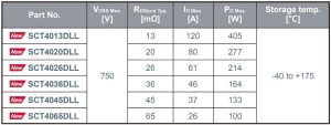
ROHM launches SiC MOSFETs in TOLL package that achieves both miniaturization and high-power capability
ROHM has begun mass production of the SCT40xxDLL series of SiC MOSFETs in TOLL (TO-Leadless) packages. Compared to conventional packages (TO-263-7L) with equivalent voltage ratings and on-resistance, these new packages offer approximately 39% improved thermal performance. This enables high-power handling despite their compact size and low profile. It is ideal for industrial equipment such as server power supplies and ESS (Energy Storage Systems) where the power density is increasing, and low-profile components are required to enable miniaturized product design.
In applications like AI servers and compact PV inverters, the trend toward higher power ratings is occurring simultaneously with the contradictory demand for miniaturization, requiring power MOSFETs to achieve higher power density. Particularly in totem pole PFC circuits for slim power supplies, often called “the pizza box type,” stringent requirements demand thicknesses of 4mm or less for discrete semiconductors.
ROHM’s new product addresses these needs by reducing component footprint by approximately 26% and achieving a low profile of 2.3mm thickness – roughly half that of conventional packaged products. Furthermore, while most standard TOLL package products are limited by a drain-source rated voltage of 650V, ROHM’s new products support up to 750V. This allows for lower gate resistance and increased safety margin for surge voltages, contributing to reduced switching losses.
The lineup consists of six models with on-resistance ranging from 13mΩ to 65mΩ, with mass production started in September 2025 (sample price: $37.0/unit, tax excluded). These products are available for online purchase from online distributors such as DigiKey, MOUSER, and Farnell. Simulation models for all six new products are available on ROHM’s official website, supporting rapid circuit design evaluation.
Product Lineup
Application Examples
・Industrial equipment: Power supplies for AI servers and data centers, PV inverters, ESS (energy storage systems)
・Consumer equipment: General power supplies
The post ROHM launches SiC MOSFETs in TOLL package that achieves both miniaturization and high-power capability appeared first on ELE Times.
📰 Газета "Київський політехнік" № 43-44 за 2025 (.pdf)
")
Вийшов 43-44 номер газети "Київський політехнік" за 2025 рік
Asia-Pacific Takes the Lead in AI Adoption Across Manufacturing
Courtesy: Rockwell Automation
Manufacturing around the world has undergone a significant transformation with the emergence of artificial intelligence (AI) and machine learning. With dynamic market conditions and pressures to optimize operations across the supply chain, more businesses today are turning to technology to meet the demands of an increasingly competitive market.
To get a better understanding of the smart manufacturing landscape and how manufacturers are leveraging these new technologies, the latest edition of the State of Smart Manufacturing report (SOSM) surveyed more than 1,500 manufacturing decision makers across industries from 17 countries, including Asia Pacific nations Australia, China, India, Japan, New Zealand, and South Korea.
Now in its 10th edition, the report offers a global perspective on today’s challenges and tomorrow’s opportunities, highlighting how smart manufacturing and emerging technologies are fostering resilience and shaping the future.
How AI is Challenging the Status Quo in the Asia Pacific
Rich in resources with the resilience to constantly adapt and innovate, Asia Pacific (APAC) is setting the pace for manufacturing and industrial growth around the world. There is strong digitization momentum across the region, as AI and smart manufacturing technologies are no longer buzzwords but have become mission-critical to drive quality, agility, and growth.
This year’s survey is proof that the focus has shifted from experimentation to execution, where more manufacturers have adopted a tech-first mindset. Nearly half of manufacturers are already scaling AI to address workforce gaps, cybersecurity risks, and evolving sustainability targets, and APAC organizations investing in generative and causal AI increased 10% year-over-year.
The growing maturity in how businesses view AI is noticeable, moving towards becoming a strategic enabler rather than a supplementary tool. Trust in AI has deepened, with 41% of those surveyed in APAC having plans to increase automation in the workplace to address workforce shortage and bridge the skills gap. Organizations are no longer primarily using AI for predictive maintenance. They are now leveraging these capabilities for other, more sophisticated, autonomous operations such as quality assurance and adaptive control, which help to reduce human error and enhance real-time decision-making.
AI in Cybersecurity
With the rapid adoption of digital technologies, cybersecurity has become a growing concern across industries, including manufacturing. Globally, it now ranks as the second most significant external obstacle for manufacturers. In the APAC region, cybersecurity is top of the list, alongside inflation and rising energy costs.
In response, businesses are accelerating their use of AI, adopting smart manufacturing technologies to digitize operations, and upskilling existing talent to stay competitive and minimize cybersecurity risks. They are also hiring with new priorities, whereby cybersecurity skills and standards have become an in-demand capability.
Understanding the need for secure-by-design architectures and real-time threat detection capabilities, Rockwell Automation has developed a series of threat intelligence and detection services, helping manufacturers to stay ahead of the evolving cybersecurity frameworks and industry standards.
Transforming the Workforce with AI
Alongside AI, the workforce, too, is evolving. Just as AI can support business needs, it requires a skilled workforce to adapt these technologies to deliver real business value. Manufacturers across APAC are looking to AI to increase automation and make workflows more efficient, while looking for employees with strong analytical thinking skills to take on more value-added tasks. While challenging, the SOSM report reveals that the need for more skilled workers is not a uniquely regional issue but a global concern, affecting industries in both developed and emerging markets.
On the upside, the skills gap in APAC has narrowed slightly from the previous year, with only 29% of respondents in 2025 citing skills gap as a challenge compared to the 31% in 2024. This suggests that investments in talent development and education are beginning to pay off.
Delivering More Sustainable Business Outcomes for the Long Run
As an industry, manufacturing consumes lots of energy. As manufacturers across the region become more invested in their ESG goals, they are driven to improve business efficiencies in pursuit of sustainability and resource conservation. Over half (55%) stated that improving efficiencies is the top reason to pursue better sustainability, up from 39% last year. By improving workflow efficiencies through automation and technologies like AI, businesses are saving on business costs while supporting better energy management.
As the 2025 State of Smart Manufacturing report shows, AI is no longer a distant promise for the Asia Pacific—it is a powerful catalyst actively reshaping how the region builds, protects, and grows. From strengthening cybersecurity and elevating workforce capabilities to enabling smarter energy use and more sustainable operations, APAC manufacturers are demonstrating what it means to move from digital ambition to digital action.
With technology adoption accelerating and confidence in AI deepening, the region is well-positioned to define the next era of global manufacturing. Those who continue to invest in talent, innovation, and secure, future-ready systems will not only overcome today’s challenges but also lead the transformation of industry for years to come.
The post Asia-Pacific Takes the Lead in AI Adoption Across Manufacturing appeared first on ELE Times.
Smartphone production grows 9% in Q3/2025, driven by seasonal demand and new product releases
День Донора 2025

День донора в КПІ ім. Ігоря Сікорського 2025 це 📌 35 учасників донорського відбору та 🩸 11,25 літрів крові!!!
Pages


![[link]](https://i.redd.it/4fcpb4o58a5g1.jpeg)
![[link]](https://i.redd.it/tg8juj32c95g1.jpeg)