
Feed aggregator
Will AI Consume the World’s Electricity? Addressing AI Data Center Demands with Advanced Power Semiconductors
Courtesy: RoHM
AI’s unprecedented advancement is reshaping our world, but this transformation comes with the urgent challenge of sharply rising energy demands from data center infrastructure.
In response, Japan has launched an ambitious national strategy—the ‘Watt-Bit Initiative’—spearheaded by the Ministry of Economy, Trade, and Industry (METI). This comprehensive program aims to establish Japan as a global leader by developing ultra-efficient data centers strategically distributed across the nation. Through collaborative platforms like the ‘Watt-Bit Public-Private Council,’ METI is orchestrating a unified effort among key sectors—energy providers, telecommunications, data center operators, and semiconductor manufacturers—to turn this vision into reality.
Will AI Consume the World’s Electricity?
The explosive growth of generative AI technologies like ChatGPT has triggered an unprecedented surge in data center energy demands. Training and inference of complex AI models require enormous computational resources, supported by high-performance servers operating continuously around the clock.
This escalating demand for electricity not only places a significant strain on local environments but also raises concerns about the stability of the power supply. As AI continues to advance, the limitations of conventional power supply systems are becoming increasingly apparent.

Against this backdrop, three urgent challenges emerge: improving energy efficiency, expanding the use of renewable energy, and optimizing the regional distribution of data centers. Achieving a sustainable society requires moving away from fossil fuel dependency and embracing renewable sources such as solar and wind power.
Utilizing Renewable Energy in Data Centers
Data centers, now an indispensable part of modern infrastructure, are at a major turning point.
Traditionally, urban data centers have been concentrated in metropolitan hubs like Tokyo to ensure low-latency communication for services requiring high-speed data access, including finance, healthcare, and edge computing. However, the surge in power consumption driven by AI adoption, coupled with the need for robust business continuity (BCP) in the face of large-scale natural disasters, is accelerating the shift toward decentralizing data centers into suburban areas.

These new sites offer compelling advantages beyond just abundant available space. They enable seamless integration of renewable energy sources such as solar and wind power, benefit from surplus grid capacity for stable electricity, and leverage natural cooling from climate and water resources, dramatically reducing operational costs. As a result, suburban facilities are increasingly being adopted for modern workloads such as cloud hosting, backup, disaster recovery, and large-scale storage.
The Future of Server Rack Expansion
Urban data centers face severe land constraints, and even suburban data centers, where securing large plots is relatively easier, are approaching their limits in available space for server deployment.
To overcome this, server racks are evolving into high-density AI server racks designed to house a greater number of high-performance servers efficiently. Rather than expanding the total number of server racks, the industry is moving toward high-density configurations equipped with more CPUs, GPUs, and other functional boards, significantly boosting the computing power per rack to maximize performance within limited space.

While the external appearance of server racks remains largely unchanged, their internal storage capacity has increased several fold.
This leap in performance and density demands a fundamental transformation of power delivery systems. Conventional multi-stage power conversion introduces significant energy losses, making efficient supply increasingly difficult. As a result, innovations such as reducing conversion stages and adopting high-voltage direct current (HVDC) architectures are gaining momentum, driving the need for SiC and GaN power semiconductors. ROHM, together with other industry leaders, is advancing technologies that support this transformation, enabling both higher performance and greater energy efficiency across entire data centers.
- Are Today’s Power Systems Sufficient?
The sharp rise in power consumption of high-performance AI servers—particularly GPUs—is forcing a fundamental redesign of existing data center power architectures. Conventional multi-stage power conversion incurs significant conversion losses, making efficient power delivery increasingly difficult.

In today’s data centers, high-voltage AC is supplied and gradually stepped down through multiple transformers and rectifiers before finally being converted into the low-voltage DC required by servers. Each stage of this process incurs losses, ultimately reducing overall efficiency. To address these challenges, data centers are expected to undergo key transformations aimed at enhancing both power conversion efficiency and reliability.
- Reducing Power Conversion Stages
A growing trend is the integration of multiple conversion processes—for example, converting high-voltage AC directly to DC, or stepping down high-voltage DC directly to the voltage used by servers. This approach significantly reduces the number of conversion steps, minimizing energy losses, enhancing overall system efficiency, and lowering the risk of failures.
- Supporting High-Voltage Input/High-Voltage Direct Current (HVDC) Power Supplies
Server rack input voltages are shifting from traditional low-voltage 12VDC and 48VDC to higher levels such as 400VDC, and even 800VDC (or ±400VDC). Operating at higher voltages reduces transmission current, enabling lighter busbar designs.
At the same time, the adoption of HVDC systems is gaining momentum. Unlike conventional AC-based architectures, HVDC delivers DC power directly to server racks, reducing the need for multiple AC/DC conversion stages. This approach enhances energy efficiency, enables more flexible power management and bidirectional transmission, and simplifies integration with renewable energy sources.
- Increasing Adoption of SSTs (Solid State Transformers)
Transformer equipment is evolving from traditional designs to SSTs (Solid State Transformers) that leverage semiconductor technology. SSTs are expected to play a key role in significantly miniaturizing conventional equipment.
- Growing Demand for SiC/GaN Power Semiconductors
Building high-efficiency, high-voltage power systems requires performance levels that exceed the capabilities of conventional silicon (Si) semiconductors. This has made SiC and GaN power semiconductors indispensable. These advanced devices enable low-loss, high-frequency, high-temperature operation under high-voltage input conditions, greatly contributing to both the miniaturization and efficiency of power systems.

Moreover, as these technologies advance, their benefits extend beyond power systems to individual devices within server racks, further improving overall energy efficiency.
ROHM is accelerating the development of solutions for next-generation servers. In addition to existing products such as SiC/GaN/Si IGBTs, isolated gate drivers, cooling fan drivers, SSD PMICs, and HDD combo motor drivers from the EcoSiC, EcoGaN, and EcoMOS series, we are also developing high-current LV MOS, isolated DC-DC converters, DC-DC converters for SoCs/GPUs, and eFuses.
Power Semiconductors Driving Next-Generation AI Data Centers
- SiC Devices Ideal for High Voltage, Large Current Applications
SiC devices are particularly well-suited for sets requiring high voltages and currents. As server rack input voltages continue to rise, conventional 54V rack power systems face increasing challenges, including space limitations, high copper usage, and significant power conversion losses.
By integrating ROHM’s SiC MOSFETs into next-generation data center power systems, superior performance can be achieved in high-voltage, high-power environments. These devices reduce both switching and conduction losses, improving overall efficiency while ensuring the high reliability demanded by compact, high-density systems.
This not only minimizes energy loss but also reduces copper usage and simplifies power conversion across the entire data center.
- GaN Devices that Provide Greater Efficiency and Miniaturization
While SiC excels in high-voltage, high-current applications, GaN demonstrates outstanding performance in the 100V to 650V range, providing excellent breakdown strength, low on-resistance, and ultra-fast switching.
AI servers process far greater volumes of data than general-purpose servers, requiring high-performance GPUs, large memory capacity, and advanced software. This leads to higher power consumption, making efficient cooling and thermal management increasingly critical.
To address these challenges, GaN HEMTs – capable of high-speed switching (high-frequency operation) – are being integrated into power supply units to minimize power loss. This delivers major gains in power conversion efficiency, translating to substantial energy savings, lower operating costs, and reduced environmental footprint.
What’s more, GaN devices offer high current density, enabling a size reduction of approximately. 30-50% compared to conventional silicon devices. This not only improves space efficiency in power supplies and chargers, but also simplifies thermal design.
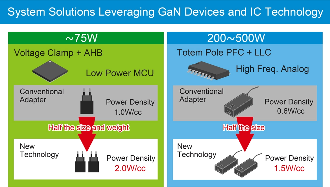
By reducing unit size and making effective use of freed-up space, the load on cooling systems can be alleviated, supporting overall system miniaturization and improved reliability. In addition, GaN’s high durability and suitability for high-frequency applications make it an ideal choice for data centers.
ROHM has succeeded in shortening the pulse width to as little as 2ns utilizing proprietary Nano Pulse Control technology, further enhancing the switching performance of GaN devices. Through the EcoGaN series, ROHM is expanding its lineup to meet the needs of AI data centers demanding compact, highly efficient power systems. The portfolio includes 150V and 650V GaN HEMTs, gate drivers, and integrated solutions that combine these components.
Conclusion
The evolution of AI, which shows no signs of slowing, comes with an inevitable surge in power demand.
According to the International Energy Agency (IEA), global data center electricity consumption is expected to more than double in the next 5 years, reaching approximately 945 billion kWh. Around half of this demand is projected to be met by renewable energy sources such as solar and wind, signaling a major shift in how energy is generated and consumed in the power-hungry data center sector. Technologies like photovoltaics (PV) and energy storage systems (ESS) are gaining traction as essential components of this transformation.
ROHM is actively contributing to this transition with a broad portfolio of advanced power semiconductor technologies, including SiC and GaN devices. These solutions enable high-efficiency power systems tailored for next-generation AI data centers. ROHM is also accelerating the development of new products to meet evolving market needs, supporting a more sustainable and prosperous AI-driven future.
The post Will AI Consume the World’s Electricity? Addressing AI Data Center Demands with Advanced Power Semiconductors appeared first on ELE Times.
Filtronic awarded £1.2m funding to develop 550W Ka-band solid-state power amplifiers
STMicroelectronics streamlines smart-home device integration with industry-first Matter NFC chip
STMicroelectronics has unveiled a secure NFC chip designed to make home networks faster and easier to install and scale, leveraging the latest Matter smart-home standard. ST’s ST25DA-C chip lets users add lighting, access control, security cameras, or any IoT device to their home network in one step by tapping their phone. The chip is the first commercial solution fulfilling newly published enhancements in Matter—the latest open-source standard now making smart home devices secure, reliable, and seamless to use.
“The integration of NFC-based onboarding in Matter 1.5 is a timely enhancement to the smart home experience. Our market-first ST25DA-C chip leverages this capability to simplify device commissioning through tap-to-pair functionality. This reduces setup complexity, especially for installations that are difficult to access, thanks to NFC-enabled battery-less connectivity. This aligns well with the broader momentum in the smart home market to serve consumers who increasingly prioritize ease of use, interoperability, and security. NFC-enabled Matter devices are positioned to play a key role in driving even greater adoption,” said David Richetto, Group VP, Division General Manager, Connected Security at STMicroelectronics.
“Matter is an important standard for the smart-home industry, enabling seamless communication across devices, mobile apps, and cloud services. Its primary benefit is simplifying technology for non-expert consumers, which could help accelerate adoption of connected devices. The new STMicroelectronics’ ST25DA-C secure NFC chip is one example of next generation chipset that supports this standard, providing device makers with tools to develop the next generation of smart-home products,” said Shobhit Srivastava, Senior Principal Analyst at Omdia.
Technical information
Enhanced usability: ST’s new NFC Forum Type 4 chip significantly improves the user experience, leveraging NFC technology present in most smartphone devices. NFC-enabled device commissioning is faster, more reliable, and secure compared to conventional pairing using technologies such as Bluetooth® or QR codes, which are not always possible.
The ST25DA-C secure NFC tag can operate cryptographic operations required for Matter device commissioning using energy harvesting from the RF field. This mechanism allows users to jump-start adding unpowered devices to the smart home network. It also simplifies the installation of multiple accessories in parallel.
Focused on security: The ST25DA-C brings strong security to smart homes, leveraging ST’s proven expertise in embedded secure elements for protecting assets with device authentication, secure storage for cryptographic keys, certificates, and network credentials.
Based on Common Criteria-certified hardware, the ST25DA-C also targets certification to the GlobalPlatform Security Evaluation Standard for IoT Platforms (SESIP level 3).
The post STMicroelectronics streamlines smart-home device integration with industry-first Matter NFC chip appeared first on ELE Times.
Mitsubishi Electric India to Showcase Breakthrough Power Semiconductor Technologies at PCIM India 2025
Mitsubishi Electric India, is set to introduce its flagship cutting edge Power Semiconductor Devices and technology to the Indian market. MEI Participation in PCIM Asia New Delhi 2025 reinforces the company’s commitment on delivering high-efficiency semiconductor solutions to support India’s growing demand in the area of Home appliances, Railway, xEV, renewable energy and industrial Applications.
Visitors at PCIM India 2025 will experience the new DIPIPM platform that integrates inverter circuitry, gate-drive functions and protection features into a single module. These modules enable compact designs and improved system safety. Available in both IGBT and SiC-based versions, the latest Compact DIPIPM and SLIMDIP families are suited for applications such as room air conditioners, washing machines, commercial HVAC, solar pumping and light industrial drives.
Mitsubishi Electric India will also showcase a wider product portfolio, including high-voltage HVIGBT modules, LV100 and NX industrial power modules, and automotive-grade semiconductor platforms engineered for Utility-scale solar inverters, wind converters, EV charging & powertrains, Railway traction converters, HVDC transmission and induction heating. Alongside the Power Modules, Mitsubishi Electric India will also display its latest bare-die SiC MOSFETs and RC-IGBT technology which enables optimal structure, low loss, and high reliability devices for xEV- traction and charging applications.
| Product Line | Key Features |
| DIPIPM (Dual In-line Package Intelligent Power Module) | *Offers CSTBT & RC-IGBT chip technologies in a wide line-up *Available in 600V and 1200V, 5A–100A *Includes SiC-MOSFET variants and new Compact DIPIPM & SLIMDIP series |
| LV100 & NX Power Modules | *Industry-standard IGBT & SiC modules with 7th/8th gen CSTBT chipset and SLC packaging *Voltage: 1200V/1700V/2000V; Current: 225A–1800A *Includes new 8th gen LV100 & NX models |
| HVIGBT (High-Voltage IGBT) | *Modules for traction and power transmission *Voltage options: 1700V, 3300V, 4500V, 6500V; Current: 400A–2400A *High-voltage SiC up to 3300V/175A–800A *Includes new XB Series |
| Power Modules for Automotive | *Designed with integrated cooling fins and DLB technology *The Line-up of 2 in 1 circuit & 6 in 1 circuit with latest SiC & RC-IGBT chip technologies *Available in 750V/1300V, 350A–800A with on-chip current and temperature sensing *Includes new J3 Series |
Speaking on the participation, Mr. Hitesh Bhardwaj, General Manager/Business Head, Semiconductors & Devices, Mitsubishi Electric India said: “India is entering a decisive phase of Power Electronics across mobility, renewable energy infrastructure. With the introduction of latest Si and SiC semiconductor technologies to the domestic market, we aim to empower Indian manufacturers with smarter, more efficient and more reliable technologies. Our long-term vision is to support the country’s innovation ecosystem and contribute to sustainable growth across industry and society.”
With India’s manufacturing ecosystem evolving toward higher energy efficiency standards and smarter power architectures, Mitsubishi Electric India’s latest offering strengthens access to globally proven semiconductor innovation tailored for future-ready applications.
The post Mitsubishi Electric India to Showcase Breakthrough Power Semiconductor Technologies at PCIM India 2025 appeared first on ELE Times.
ASMPT Wins New Orders for Nineteen Chip-to-Substrate TCB Tools to Serve AI Chip Market
ASMPT announced it had won new orders for 19 Chip-to-Substrate (C2S) TCB tools from a major OSAT partner of the leading foundry serving the AI chip market.
ASMPT is the sole supplier and Process of Record (POR) of C2S TCB solutions for this customer, supporting their high-volume manufacturing requirements. These latest systems will enable their next-generation C2S bonding for logic applications as compound die sizes get larger. This demonstrates the customer’s continued confidence in ASMPT’s technological leadership and production-proven capabilities. Looking ahead, ASMPT is well-positioned to secure additional orders in the future.
This continued momentum for ASMPT’s flagship Thermo-Compression Bonding (TCB) solutions reinforces its position as the industry’s leading provider of advanced packaging solutions for artificial intelligence and high-performance computing applications.
“The TCB market is experiencing transformational growth driven by AI and HPC applications,” said Robin Ng, Group CEO, ASMPT. “Our comprehensive technology portfolio spanning chip-on-wafer, chip-on-substrate, and HBM applications positions ASMPT uniquely to support our customers’ most demanding advanced packaging roadmaps. This latest win validates our technology leadership and highlights the market’s recognition of our ability to deliver production-ready, scalable platforms.”
With the largest TCB installed base worldwide consisting of more than 500 tools, ASMPT is strategically positioned to capture between 35% to 40% of an expanded TCB market. ASMPT recently expressed confidence that the TCB Total Addressable Market (TAM) projection will exceed US$1 billion by 2027, bolstered by recent news about AI ecosystem investments.
The post ASMPT Wins New Orders for Nineteen Chip-to-Substrate TCB Tools to Serve AI Chip Market appeared first on ELE Times.
Microchip Halves the Power Required to Measure How Much Power Portable Devices Consume
Battery-operated devices and energy-restricted applications must track and monitor power consumption without wasting power in the process. To solve this challenge, Microchip Technology announced two digital power monitors that consume half the power of comparable solutions based on typical operating conditions at 1024 samples per second. The PAC1711 and PAC1811 power monitors achieve this efficiency milestone while also providing real-time system alerts for out-of-limit power events and a patent-pending step-alert function for identifying variations in long-running averages.
The 42V, 12-bit single-channel PAC1711 and 16-bit PAC1811 monitors are housed in 8- and 10-pin Very Thin Dual Flat, No-Lead (VDFN) packages, respectively, that are pin- and footprint-compatible with the popular Small Outline Transistor (SOT23)-8 package. This compatibility simplifies second-sourcing for developers, while streamlining upgrades and integration into existing systems.
“Until now, portable devices and a variety of energy-constrained applications have needed to burn a significant amount of valuable power to measure how much they are consuming,” said Keith Pazul, vice president of Microchip’s mixed-signal linear business unit. “Unlike many existing solutions, Microchip’s power monitors function as independent ‘watchdog’ peripherals, eliminating the need for the MCU to handle power monitoring tasks. These monitors allow the MCU or host processor to remain dormant until a significant power event occurs such as needing an LCD screen to power on.”
The PAC1711 and PAC1811 power monitors’ step-alert capability keeps a running average of voltage and current values. If there is a significant, user-defined variation, it will notify the MCU to act on it. The devices keep a rolling average, and any new sample can trigger an alert. A slow-sample pin option is available, which can delay the power usage sampling to every eight seconds and further conserve power.
An accumulator register in the power monitor can be used to manage logistical items, track system battery aging or time to recharge, and provide the short-term historical data for long-term power usage that the MCU can be programmed to act on. Both current monitor integrated circuits sense bus voltages from 0 to 42 volts and can communicate over an I2C interface. They are well-suited for first- or second-source options in computing, networking, AI/ML and E-Mobility applications.
The post Microchip Halves the Power Required to Measure How Much Power Portable Devices Consume appeared first on ELE Times.
India needs up to 15,000 crore more investment for PCB manufacturing: JS Gujral, MD, Syrma SGS
In the budget for 2021, the Indian government sanctioned Rs. 76,000 crores for the India Semiconductor Mission (ISM). Today, after nearly five years, there is a need for an additional investment of Rs. 10,000-15,000 crores in the next two to three years to boost domestic PCB manufacturing to reduce import dependency below 50%, according to JS Gujral, MD, Syrma SGS.
Currently, India demands PCBs worth nearly Rs. 50,000 crores, and only 10% of that demand is met locally, while the rest is fulfilled through imports from China, Taiwan and other nations. The aim is to increase the production to a worth of Rs. 20,000 in the next three years when the demand itself will rise to Rs. 70,000 worth.
From the many factors holding India back, the raw material bottle neck is a significant problem. Raw materials make up for nearly 60% of the total cost of the PCB. Copper Clad Laminate (CCL) is one of the primary materials used in PCB manufacturing. It covers nearly 27% of that raw material cost. While India is gradually progressing towards its complete domestic manufacturing, there are other burdens such as the copper foil, pre pregs, and specialized chemicals. These three are largely imported which add to the exorbitant costs of PCBs manufactured in India, making them costly and less competitive in the global market.
Experts recommend the increase in domestic supply for copper foils and necessary raw materials alongside CCL to maintain the competitiveness of locally produced PCBs to meet both national and international demands.
The post India needs up to 15,000 crore more investment for PCB manufacturing: JS Gujral, MD, Syrma SGS appeared first on ELE Times.
Slim DIN Rail Power Supplies For Industrial Applications
Advertorial by RECOM
DIN rail mounting has revolutionized electrical cabinets since the idea was first conceived in the 1920s to standardize the mounting of switchgear and enable interchangeability between manufacturers. DIN stands for “Deutsche Industrie Norm” or the “German Industrial Standard” and the success of the DIN rail system rapidly spread outside of Germany, eventually becoming the European standard DIN EN 60715.
The DIN rail system’s simplicity and versatility—allowing components to be easily clicked into place or removed for maintenance—has made it the preferred standard for electrical cabinet design. As a result, manufacturers offer a wide range of DIN rail-compatible components, including circuit breakers, relays, contactors, terminal blocks, data interfaces (KNX, DALI, Ethernet), PLCs, and slim DIN rail power supplies (Figure 1).
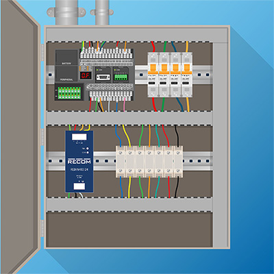 Fig. 1: Typical DIN rail installation
Advantages of the DIN Rail System
Fig. 1: Typical DIN rail installation
Advantages of the DIN Rail System
Firstly, the modular approach allows electrical cabinets and panels to be quickly assembled, moved, or rearranged for optimum use of the available space with only a standard electrician’s screwdriver as a tool. There is no drilling, cutting, or threading needed. Electrical cabinets and panels are often available with pre-installed rails so installation can begin immediately.
Secondly, the DIN rail system allows easy upgrading or repair without disrupting other components – a defective part can be simply unclipped and replaced without affecting the other components. If the new part happens to be slightly larger than the older module, then the existing components can be shifted along the rail to make space.
Thirdly, as the mounting rail dimensions are all standardized, parts from different manufacturers are interchangeable and mounting compatible. On a single rail, different electrical components can be freely mixed, so, for example, connector blocks can be placed next to power supplies to simplify the distribution of power and reduce the amount of cabling required, or actuator relays placed next to PLCs.
Fourthly, as you might expect from a German standard, the ease of mounting allows an organized, neat, and logical layout within the cabinet. This not only speeds up assembly by streamlining the whole construction process but simplifies maintenance and troubleshooting. All electrical contacts are accessible from the front without disconnecting any wiring and many electrical components have status or alarm indicators so that complex installations can be quickly inspected to find the fault.
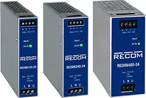 Fig. 2: REDIIN120, REDIIN240, and REDIIN480 DIN rail Power Supplies
Solutions include adding spacers between equipment to allow free air convection to cool the components, repositioning heat-generating components so that they are not in close proximity to one another, or, in extreme cases, adding fans to force-air cool the parts. The vertical separation between rails also needs to be considered so that warm air rising from one component does not adversely affect the component placed immediately above it. Fortunately, software packages are readily available that can be used to both plan the layout of the panel or cabinet in advance and to calculate the expected thermal loading. This software is often offered free by the cabinet manufacturers. More advanced software can also automatically check for compliance with electrical safety, construction, and technical standards, such as EN 61439.
RECOM is an established power supply manufacturer that is well-known for board-mounting or chassis-mounting embedded power, but also offers competitively priced AC/DC DIN rail mount power supplies (Figure 2).
Key Features of DIN Rail Power Supplies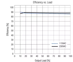 Fig. 3: Flat efficiency curve of the REDIIN120-24. No load power consumption is only 150mW
Design
Fig. 3: Flat efficiency curve of the REDIIN120-24. No load power consumption is only 150mW
Design
The products are fully certified according to international safety standards IEC/EN/UL 62368-1, IEC/EN/UL61010-1, and IEC/EN/UL/CSA61010-2-201. Electromagnetic radiated and conducted emissions are compliant with heavy industrial EN 61000-6-4 Class B Emission standard and EN 61000-6-2 Immunity standard.
The REDIIN series are designed for industrial, automation, power distribution, and test and measurement environments. These slim power supplies are ideal for applications in heavy engineering, production, home automation, data and telecom, traffic control, and water management—anywhere a compact, reliable, and cost-effective DC power supply is required within cabinets or electronic enclosures.
The post Slim DIN Rail Power Supplies For Industrial Applications appeared first on ELE Times.
Turned Commodore Plus4 Keyboard into a MIDI device.
 | Still working on the matrix mapping but it does work besides a few toasted keys. Planning to work on some chord progression/arpeggiator code and connect it to a Korg DS8 of the same era. [link] [comments] |
The Software-Defined Vehicle Revolution: The Engineering Call to Action
The global automotive industry is undergoing its most profound transformation since the assembly line. This shift, driven by electrification and autonomy, is centrally powered by the Software-Defined Vehicle (SDV). For India’s vast pool of electronics and embedded systems engineers, this shift is more than just a trend—it’s a once-in-a-generation opportunity to become a global technology powerhouse in the automotive sector.
The stakes are enormous. India’s software-defined vehicle market is projected to witness a CAGR of 16.56% during the forecast period, FY2026-FY2033, growing from USD 2.69 billion in FY2025 to USD 9.16 billion in FY2033 through hardware, software, and subscription-based features. This piece breaks down the fundamental architectural shift, the commercial imperative driving it, and the precise skills Indian engineers must master to capture this monumental value.
The Architectural Flip: From Distributed Modules to Central Compute
For the last three decades, vehicle architecture was defined by a sprawling, distributed network of Electronic Control Units (ECUs). Modern cars can contain up to 150 dedicated ECUs, each dedicated to a narrow task (such as controlling a specific window or a part of the engine), which are scattered throughout the car.
Christopher Borroni-Bird, Founder of Afreecar, USA, notes, “The path to SDVs is a major disruption for automakers. It is a fundamental shift in value from hardware to software.”
The fundamental limitations of this legacy architecture are now a critical bottleneck for innovation:
- Complexity and Cost: This highly decentralized design requires kilometers of heavy, expensive wiring and complex communication protocols (like CAN and LIN), leading to massive complexity in integration and testing.
- Bandwidth Saturation: The low bandwidth of CAN limits the data throughput required by modern systems like Advanced Driver Assistance Systems (ADAS), which process gigabytes of sensor data per second.
- Inflexible Updates: Functionality is tied tightly to hardware, making it nearly impossible to introduce meaningful new features after the car leaves the factory.
The Software-Defined Vehicle solves this by replacing the distributed ECUs with a centralized, high-performance computing (HPC) approach. It consolidates functions into powerful, centrally or zonally placed compute units. This transformation moves through two key stages:
- Domain-Centralization (The Intermediate Step)
In the domain-centralized architecture, automakers consolidate dozens of small ECUs into a handful of powerful Domain Controllers—typically one each for powertrain, body, infotainment, and ADAS. These domain controllers are high-performance SoCs that replace clusters of ECUs within each functional region. While this significantly reduces ECU count and wiring complexity, it still maintains separation between critical domains. Engineers now need to handle thermal constraints, high-speed data movement, and virtualization middleware to ensure that safety-critical functions (like braking or steering) remain strictly isolated from non-critical ones (like media playback). This stage marks the shift from distributed electronics to consolidated compute, setting the foundation for full vehicle-centralized architectures.
- High-Speed Networking
High-speed networking is essential in SDVs because modern vehicles generate enormous volumes of data from cameras, radar, LiDAR, and other sensors—far beyond what the traditional CAN bus can carry. CAN was designed for millisecond-level control signals, not multi-megabit video streams or real-time sensor fusion. To solve this bottleneck, SDVs now use Automotive Ethernet as the central data backbone. It supports gigabit-level throughput and incorporates Time-Sensitive Networking (TSN) to ensure data is delivered with guaranteed timing, which is critical for ADAS decision-making.
In simple terms: Automotive Ethernet + TSN allows the car’s brain to receive huge amounts of sensor data quickly, predictably, and without delay—something CAN was never built for. This shift enables reliable perception, faster response times, and the scalable communication architecture required for autonomous and software-defined features.
The Commercial Imperative: Recurring Revenue and Lifetime Value
The architectural shift is driven equally by a dramatic change in the business model. Historically, an OEM’s revenue ceased the moment the car was sold. SDVs flip this model, transforming the vehicle into an evolving platform for recurring revenue. The technical architecture in SDVs is merely the enabling layer for an entirely new economic model. When a vehicle’s capabilities are defined by its software stack, the relationship with the customer becomes continuous.
The market potential for subscriptions, services, and features-on-demand is what drives the massive industry investment. Post-sale monetization opportunities include:
- Features-as-a-Service: Performance boosts, advanced ADAS capabilities, or heated seats activated temporarily via a subscription.
- Predictive Maintenance: Using vehicle data to predict failures, leading to service revenue and higher customer satisfaction.
- In-Car Commerce and Telematics: Partnerships for payment processing, insurance optimization, and fleet management services.
The Pillars of SDV Engineering: New Skill Requirements
To build the SDV, engineers must shift their focus from optimizing individual microcontrollers to designing entire systems based on high-performance computing, security, and real-time networking. The core skill pillars for the next generation of Indian automotive engineers are:
- High-Speed, Deterministic Networking
The shift from CAN/LIN (up to 1 Mbit/s) to Automotive Ethernet (100 Mbit/s to 10 Gbit/s) is essential to handle the massive data from LIDAR, radar, and HD cameras. Crucially, engineers must master Time-Sensitive Networking (TSN). TSN is the standard that guarantees deterministic data delivery—meaning a brake command always arrives in a precise, guaranteed timeframe, regardless of network traffic. This is a non-negotiable requirement for functional safety.
- Platform Virtualization and Mixed-Criticality Systems
The HPC runs software with varying safety requirements, known as mixed-criticality systems. A malfunction in the display stack must not crash the brake-by-wire system. This separation is achieved using two key technologies:
- Hypervisors (Type 1): Specialized hypervisors allow multiple operating systems (or execution environments) to run concurrently on the same HPC hardware, ensuring fault isolation and resource partitioning.
- Adaptive AUTOSAR: This next-generation middleware (replacing Classic AUTOSAR) is built to manage the complexity of centralized compute, supporting POSIX-compliant operating systems and service-oriented communication protocols necessary for dynamic, interconnected applications.
3. Functional Safety and Cybersecurity
With software controlling all critical systems, safety standards must be integrated at every layer of the architecture.
- ISO 26262 (Functional Safety): Engineers need proficiency in defining and implementing specific Automotive Safety Integrity Levels (ASIL) for every function. For example, ADAS features might require ASIL-D (the highest level).
- ISO/SAE 21434 (Cybersecurity): Connectivity exposes the vehicle to external threats. Expertise in Threat Analysis and Risk Assessment (TARA), secure boot, intrusion detection systems (IDS), and over-the-air (OTA) update security is mandatory to protect the vehicle throughout its 15-year lifecycle.
India’s Strategic Advantage and the Talent Gap
India is uniquely positioned to capitalize on this shift. The country already hosts the largest R&D and engineering centers outside of headquarters for nearly every global OEM and Tier-1 supplier (e.g., Bosch, Continental, Mercedes-Benz, Hyundai). Indian teams are already responsible for complex areas like Infotainment development, diagnostics, and component-level software.
However, a critical gap exists between foundational embedded skills and the advanced, systems-level expertise required for SDVs. The shortage is most acute in:
- System Architects: We need engineers who can define the holistic E/E architecture, not just code a single ECU. This requires an end-to-end view of hardware, software, networking, and safety protocols.
- High-Level Software (Full-Stack Automotive): Expertise in integrating cloud services (AWS, Azure) with the in-vehicle VOS, leveraging DevOps pipelines, and managing vast data streams for machine learning models running on the car’s edge processors.
- Low-Level Middleware and Safety: Deep competence in Adaptive AUTOSAR and hypervisor configuration, which allows the critical and non-critical software stacks to coexist safely.
The Call to Build
The SDV revolution demands that Indian engineers make a proactive pivot. The value chain is restructuring, and the future winners will be those who design the platforms, not just those who implement modules.
This transition requires investment—not just by multinational corporations, but by individual engineers and educational institutions. Universities must rapidly introduce a curriculum focused on high-speed communications (TSN), virtualization, and modern safety standards. Industry professionals must aggressively pursue certifications and hands-on experience in Adaptive AUTOSAR and HPC environments.
India has the talent base and the sheer numbers to become the world’s SDV hub. This opportunity is about moving up the value chain, leading innovation, and defining the future of mobility from Bengaluru, Pune, and Hyderabad. The vehicle is being redefined, and with the right strategy and swift action, Indian engineers can and must be the global architects of the Software-Defined Vehicle era.
The post The Software-Defined Vehicle Revolution: The Engineering Call to Action appeared first on ELE Times.
Vishay launches 1200V SiC MOSFET power modules in MAACPAK PressFit package
US ITC preliminary determination finds violation of Infineon patent by Innoscience
Ascent provides space company with PV modules for power generation testing in cislunar space
Simulación de una ALU de 16 bits en Proteus
 | Diseñé y simulé una ALU de 16 bits en Proteus, capaz de ejecutar operaciones AND, OR, XOR, SUMA y RESTA (con acarreo). Todo está organizado en módulos para facilitar el análisis, e incluye flags e indicadores para validar el comportamiento de cada operación. Si desean obtener el archivo de simulación, pueden escribirme directamente. [link] [comments] |
LED Fade in
 | Turning led on slowly [link] [comments] |
🍎 День відкритих дверей KPIAbitFest

КПІ ім. Ігоря Сікорського запрошує учнів старших класів ваших закладів освіти долучитися до Дня відкритих дверей — KPIAbitFest, який відбудеться 13 грудня з 10:00 до 13:00 у Бібліотеці КПІ ім. Ігоря Сікорського (проспект Берестейський, 37).
Випускник КПІ увійшов до рейтингу Clarivate найбільш цитованих учених

Юрій Гогоці, професор Університету Дрекселя (США) і випускник Київського політехнічного інституту імені Ігоря Сікорського, увійшов до списку Clarivate найцитованіших дослідників світу у 2025 році.
Nuvoton launches compact 1.7W 402nm violet laser in TO-56 CAN package
A digital filter system (DFS), Part 1

Editor’s note: In this Design Idea (DI), contributor Bonicatto designs a digital filter system (DFS. This is a benchtop filtering system that can apply various filter types to an incoming signal. Filtering range is up to 120 kHz.
In Part 1 of this DI, the DFS’s function and hardware implementation are discussed.
In Part 2 of this DI, the DFS’s firmware and performance are discussed.
Selectable/adjustable bench filterOver the years, I have been able to obtain a lot of equipment needed for designing, testing, and diagnosing electronic equipment. I have accumulated power supplies, scopes, digital voltmeters (DVMs), spectrum analyzers, signal generators, vector network analyzers (VNAs), LCR meters, etc., etc.
One piece of equipment I never found is a reasonably priced lab bench filter—something that would take in a signal and filter it with a filter whose parameters could be set on the front panel.
There are some tools that run on a PC’s sound card, but I don’t like to connect my electronic tests on my PC for fear that I’ll damage the PC. The other issue is that I am looking for something that can go up to 100 kHz or so, which is not typical of many soundcards. So, it was time to try to design one.
Wow the engineering world with your unique design: Design Ideas Submission Guide
What I came up with in a small bench-top device with one BNC input for the signal you want filtered and one BNC output for the resulting filtered signal (Figure 1). It has a touchscreen LCD to select a filter type and the cutoff/center frequency. So, what can it do?
 Figure 1 The finished digital filter system that allows you to select a low-pass, high-pass, band-pass, or band-stop filter type.
You can select a low-pass, high-pass, band-pass, or band-stop filter type. The filter can also be either a two-pole Butterworth or a four-pole.
For the frequency, you can select anywhere from a few Hz to 120 kHz. The are also three gain controls (an analog input gain knob, an analog output gain, and an internal digital gain.)
The cost to build the filter is around $75, as well as some odds and ends you probably already have around.
I also included a download for a 3D printable enclosure. Let’s take a deeper look at this design.
The circuitThe design is centered around a digital filter executed in a Cortex M4 microcontroller (MCU). The three main blocks of the system are an analog front end (AFE), which is composed of four op-amps providing input gain adjustment and antialiasing filtering.
Next is a single board computer (SBC) powered by a Cortex M4. This provides an input for the ADC, controls the LCD and touchscreen, executes the digital filters, and controls the output DAC.
The last block is the analog back end (ABE), which again consists of four op-amps that make up the analog gain circuit and the analog output reconstruction filter.
Let’s take a look at the schematic to see more detail (Figure 2).

Figure 2 The DFS schematic showing the AFE, the ABE, and SBC that provides an input for the ADC, controls the TFT display, executes the digital filters, and controls the output DAC.
Here you can see the blocks we just talked about and a few other minor pieces. Let’s dive a little deeper.
The AFEThe AFE starts by AC-coupling the external signal you want to filter. Then, the first op-amp, after the protection diodes, provides an adjustable gain for the input. This uses a simple single-supply inverting op-amp circuit. RV1 is a potentiometer on the front panel (see Figure 1 above) that allows for a gain of the input from 1x to 5x.
Again, looking at the schematics, we next see a single-pole low-pass filter, which is tuned to 120 kHz. Next are a pair of 2-pole Sallen-Key low-pass filters with components selected to create a Butterworth filter set to 120 kHz.
So now our input signal has been filtered at a frequency that will allow the MCU’s ADC to sample without aliasing. I designed this filter and the ABE filter using TI’s WEBENCH Circuit Designer.
So, we have a 5-pole low-pass filter frontend that will give us a roll-off of 30 dB per octave, or 100 dB per decade.
The flywheel RC circuit is next. As explained in a previous article, the capacitor in this RC circuit provides a charge to hold up the voltage level when the ADC samples the input. More on this can be found at: ADC Driver Ref Design Optimizing THD, Noise, and SNR for High Dynamic Range
The ABEWe’ll skip the MCU for now and jump to the right side of the schematic. Here we see a circuit very similar to the AFE, but this is used as a reconstruction filter that removes artifacts created by the discrete steps used in the MCU’s DAC.
So, starting from the DAC output from the SBC, we see an adjustable gain stage which allows the user, via the output potentiometer, to increase the output level, if desired. This output gain can be adjusted from 1x to 5x.
Next in the schematic, you’ll see two stages of two-pole Sallen-Key low-pass filters configured exactly like the pair in the AFE. So again, they are configured as a 120 kHz Butterworth filter.
The last op-amp circuit in the ABE is a 2x gain stage and buffer. Why a 2x gain stage? I’ll explain more later, but the gist is that the DAC has a limited slew rate compared to the sample rate I used. So, I reduced the value in the DAC by 2 and then compensated for it in this gain stage.
A note about the op-amps used in this design: The design calls for something that can handle 120 kHz passing through a gain of up to 5 and also dealing with the Sallen-Key filters (the TI WEBENCH shows a gain-bandwidth requirement of at least 6 MHz). I also needed a slew rate that could deal with a 120 kHz signal with a level of 3.3 Vpp. The STMicroelectronics TSV782 fit the bill nicely.
The last two components are the resistor and the capacitor before the output BNC connector. The resistor is used to stabilize the op-amp circuit if the output is connected to a large capacitance load. The 1uF capacitor provides AC coupling to the output BNC.
The MCUThe brains used in this design is a Feather M4 Express SBC, which contains a Microchip Technology’s ATSAMD51 that has a Cortex M4 core. This is primarily powered by a USB connection (or a battery we will discuss in Part 2).
This ATSAMD51 has a few ADCs and DACs, and we use one of each in this design. It also has plenty of memory (512 kB of program memory and 192 kB of SRAM).
It runs at a usable 120 MHz and is enhanced with a floating-point processor. All this works nicely for the digital filtering we will explain in Part 2. Other features I used include a number of digital I/O ports, an SPI port, and a few other ADC inputs.
One feature I found very nice on the SBC was a 3.3 VDC linear regulator that not only powers the MCU, but has sufficient output to power all other devices in the design.
On the schematic (Figure 1), you can see that the AFE connects to an ADC input on the SBC, and an SBC DAC connects to the ABE circuit. Another major component is the TFT LCD and touchscreen, powered by the 3.3 VDC coming from the SBC.
Miscellaneous schematic itemsThat leaves a few extra items on the schematic.
Voltage referenceThere are 2 simple ½ voltage dividers to generate 1.65 VDC from the 3.3 VDC supply. One is used on the AFE to get a mid-voltage reference for the single supply op-amp design. This reference is simply two equal resistors and a capacitor connected to ground, and from the center of the series-connected resistors.
A second reference was created for the ABE circuit. I used two references as I was laying this out on a protoboard, and the circuits were separated by a significant distance (without a ground plane).
LED indicatorThere is also an LED used to indicate that the ADC is clipping the signal because the input is too large or too small. Another LED indicates the DAC is clipping for the same reasons. There will be more discussion on this in the firmware section in Part 2.
Floating groundAn interesting feature of the SBC is that it contains the charging circuit for a lithium polymer 3.7-V battery. This is optional in the design, but it does allow you to operate the DFS with a floating ground and a quiet voltage supply, which may help in your testing.
EnableA somewhat unique feature, which turns out to be helpful, is an enable that is used to turn off the system if you pull it to ground.
If you use a battery, along with the USB, and want to use a typical power on/off switch, you would need to break the incoming USB line and the battery line, which makes it a 2-pole switch.
So, to get the DFS to power down, I pull the enable line to ground using a 3-pole SPDT switch, which I found has the typical “O/I” on/off indications. You can use a SPST switch; this will have to be switched to “I” to shut it down and “O” to turn it on.
USB voltage displayA ½ voltage divider, with a filter capacitor, is connected to the USB input and used as an input to one of the ADCs, so we can display the connected USB voltage.
Optional resetThe last item is an optional reset. I did not provide a hole to mount a pushbutton, but you can drill a hole in the back of the enclosure for a normally-open pushbutton.
More informationThis device is a fairly easy to build. I built the circuit on a protoboard with SMT parts (thru-hole would have been easier). Maybe someone would like to lay out a PCB and share the design. I think you’ll find this DFS has a number of uses in your lab/shop.
The schematic, code, 3D print files, links to various parts, and more information and notes on the design and construction can be downloaded at: https://makerworld.com/en/@user_1242957023/upload
Editor’s Note: Stay tuned for Part 2 to learn more about the device’s firmware.
Damian Bonicatto is a consulting engineer with decades of experience in embedded hardware, firmware, and system design. He holds over 30 patents.
Phoenix Bonicatto is a freelance writer.
Related Content
- Non-linear digital filters: Use cases and sample code
- A beginner’s guide to power of IQ data and beauty of negative frequencies – Part 1
- A Sallen-Key low-pass filter design toolkit
- Designing second order Sallen-Key low pass filters with minimal sensitivity to component tolerances
- Toward better behaved Sallen-Key low pass filters
- Design second- and third-order Sallen-Key filters with one op amp
The post A digital filter system (DFS), Part 1 appeared first on EDN.
Silly simple precision 0/20mA to 4/20mA converter

This Design Idea (DI) offers an alternative solution for an application borrowed from frequent DI contributor R. Jayapal, presented in: “A 0-20mA source current to 4-20mA loop current converter.”
It converts a 0/20mA current mode input, such as produced by some process control instrumentation, into a standard industrial 4/20mA current loop output.
Wow the engineering world with your unique design: Design Ideas Submission Guide
Figure 1 shows the circuit. It’s based on a (very) old friend—the LM337 three-legged regulator. Here’s how it works.

Figure 1 U1 plus R1 through R5 current steering networks convert 0/20mA input to 4/20mA output.
The fixed resistance of the R1 + R2 + R3 series network, working in parallel with the adjustable R4 + R5 pair, presents a combined load of 312 ohms to the 1.25v output of U1. That causes a zero-input current draw of 1.25/312 = 4 mA, trimmed by R5 (see calibration sequence detailed later).
Summed with this is a 0 to 16 mA current derived from the 0 to 20 mA input, controlled by the 4:1 ratio current split provided by the R1/R2/R3 current divider and fine trimmed by R2 (ditto).
Note that 4 mA is below the guaranteed minimum regulation current specification for the LM337. In fact, most will work happily with half that much, but you might get a greedy one. So just be aware.
The result is a precision conversion of the 0 to 20mA input to an accurate 4 to 20mA loop current. Conversion precision and stability are insensitive to R2 trimmer wiper resistance due to the somewhat unusual input topology in play.
Calibration proceeds in a four-step linear (iteration-free one-pass) sequence consisting of:
- Set input = 0.0 mA.
- Adjust R5 for 4.00 mA loop current.
- Set input = 20.00 mA.
- Adjust R2 for 20.00 mA loop current.
Done.
The input voltage burden is a negative 1.0 volt. The output loop voltage drop is 4 volts minimum to 40 volts maximum. The maximum ambient temperature (with no U1 heatsink) is 100oC. Resistors should be precision types, and the trimmer pots should be multiturn cermet or similar.
Stephen Woodward’s relationship with EDN’s DI column goes back quite a long way. Over 100 submissions have been accepted since his first contribution back in 1974.
Related Content
- A 0-20mA source current to 4-20mA loop current converter
- A two-wire temperature transmitter using an RTD sensor
- Two-wire interface has galvanic isolation
- Low-cost NiCd battery charger with charge level indicator
- Single phase mains cycle skipping controller sans harmonics
- Two-wire remote sensor preamp
The post Silly simple precision 0/20mA to 4/20mA converter appeared first on EDN.
Pages


![[link]](https://i.redd.it/42byuxq9v05g1.jpeg)