
Feed aggregator
Top 10 Reinforcement Learning Applications and Use Cases
One of the most intriguing areas of machine learning is reinforcement learning (RL), in which agents interact with their surroundings and acquire the best behaviors through trial and error. RL is perfect for resolving complicated, real-world issues because, in contrast to classical supervised learning, it flourishes in dynamic, uncertain environments. Reinforcement learning is reshaping how machines make decisions, driving innovation in areas such as autonomous vehicles and tailored healthcare solutions. The top 10 notable applications that highlight the strength and adaptability of reinforcement learning will be explored in this article.
- Autonomous Vehicles
RL empowers autonomous vehicles to make intelligent decisions in real time, enabling them to navigate complex and ever-changing environments—such as congested traffic or unpredictable road conditions with greater precision and adaptability.
- Predictive Maintenance
With reinforcement learning, predictive maintenance could figure out when a machine is most likely to break down, to get it fixed bait time. With that, the RL agents comprehend when equipment failure might occur by learning from past reports and further optimizes maintenance scheduling to reduce downtime and save repair costs.
- Personalized Recommendations
Reinforcement learning is employed by streaming platforms such as Netflix, and e-commerce giants such as Amazon, to customize recommendations, adapting to the evolving preferences of a user, and learning which content or products an individual is most likely to engage with.
- Healthcare Treatment Planning
RL is revolutionizing personalized medicine to assist clinicians in determining the best therapeutic strategy. It can also be used for radiation therapy, drug dose optimization, and robotic-assisted surgeries to achieve better outcomes at lower risks.
- Energy Management in Grids
Reinforcement learning(RL) helps optimize energy consumption in smart buildings and grids. By learning patterns of usage and environmental conditions, the systems adjust heating, cooling, and lighting to avoid wastage. Such measures reduce costs.
- Supply Chain and Inventory Optimization
RL-based systems help retailers and logistics companies maintain inventory levels, forecast demand, and optimize delivery routes, lowering operational costs while increasing levels of customer satisfaction.
- Robotics and Automation
In robotics, RL allows machines to acquire the skills required to perform complex tasks such as walking, grasping, and assembling objects. Manufacturing, space, and domestic robots rely on these types of skills.
- Financial Trading and Portfolio Management
RL systems allow creation of trading and portfolio management strategies adapted to the fluctuations of markets. They may improve risk management, increase returns, and support decision-making in volatile environments.
- Drone and Aerospace Navigation
With reinforcement learning, it is possible for drones and space vehicles to autonomously plan routing, collision avoidance, and adaptiveness to environmental changes. This feature is highly potential in scenarios where human intervention is limited or impossible.
- Natural Language Processing (NLP)
In NLP, the chatbot and virtual assistant are fine-tuned by reinforcement learning methods to produce a more coherent and context-aware response. It is also applied in such areas as training translation, summarization, and sentiment analysis models.
Conclusion:
Reinforcement Learning is more than just a theoretical concept it’s a transformative force across industries. Its ability to learn from interaction and adapt to change makes it uniquely suited for solving problems that traditional algorithms struggle with. As reinforcement learning (RL) continues to advance, it is expected to unlock increasingly ground-breaking applications that redefine the capabilities of machines. Whether one is a researcher, developer, or simply an intrigued observer, RL remains a dynamic and promising field that merits close attention and exploration.
The post Top 10 Reinforcement Learning Applications and Use Cases appeared first on ELE Times.
How TVS Electronics is Transforming Digital India with “Make in India” AIDC
In the fast-paced world of digital transformation, Automatic Identification and Data Capture (AIDC) has moved beyond just scanning barcodes it is now driving intelligent business outcomes powered by AI, IoT, 5G, and cloud. At the forefront of this transformation is Mr. Chakravarthy Balaji, Chief Business Officer and Vice President Products & Solutions Group (PSG Business) at TVS Electronics (TVSE).
With nearly two decades of leadership at TVSE, Mr. Balaji has played a pivotal role in reshaping the company’s growth trajectory from finance operations to leading large-scale product innovations.
In this exclusive interview with ELE Times, Mr. Balaji shares insights on how AIDC is evolving with next-gen technologies, the role of cloud-native analytics, and how TVS Electronics is positioning itself to lead the next wave of Industry 4.0 adoption in India. Excerpts:
ELE Times: How is Advanced AIDC evolving with AI, IoT, and Industry 4.0?
C. Balaji: Advanced AIDC is shifting from simple data capture to intelligent data interpretation. With AI, IoT, and Industry 4.0, it now enables predictive insights, real-time visibility, and autonomous decision-making across industries.
ELE Times: What role do cloud-native integration and real-time analytics play in driving digital transformation through AIDC?
C. Balaji: Cloud-native AIDC ensures scalability and agility, while real-time analytics converts raw data into actionable insights. Together, they drive faster decisions, process transparency, and end-to-end digital transformation.
ELE Times: What makes TVS Electronics’ ‘Make in India’ AIDC solutions stand out technologically?
C. Balaji: Our AIDC solutions are rugged, reliable, and designed for Indian conditions while meeting global standards. With launches like industrial-grade label printers, scanners, fixed scanners, and enterprise mobile computers such as HS65 and T1 Pro, we combine strong R&D, local innovation, and pan-India service support to deliver true “Make in India” excellence.
ELE Times: What role is TVS Electronics playing in leveraging AIDC to drive digital transformation across industries?
C. Balaji: TVS Electronics is enabling enterprises across retail, logistics, manufacturing, and healthcare with end-to-end AIDC solutions. We act as a solutions partner, aligning technology with business outcomes and industry digital roadmaps.
ELE Times: Which emerging technologies (AI, IoT, 5G, cloud) are most critical for the future of AIDC-led transformation?
C. Balaji: AI, IoT, 5G, and cloud are converging to redefine AIDC. Together, they transform AIDC from a data enabler into a decision enabler, powering the next wave of digital enterprises.
ELE Times: How is TVS Electronics preparing its products and services to address the next wave of digital transformation needs?
C. Balaji: We are expanding our portfolio with industrial-grade label printers, advanced scanners, fixed-position devices, and mobility solutions like HS65 and T1 Pro. Alongside, we are building partnerships in AI, IoT, and cloud to deliver future-ready, scalable, and customer-centric solutions for Industry 4.0.
The post How TVS Electronics is Transforming Digital India with “Make in India” AIDC appeared first on ELE Times.
Silanna UV’s next-gen SF2 230nm far-UVC LED doubles radiant intensity
Lotus Microsystems and EDOM Technology Form Strategic Distribution Partnership to Expand Presence Across APAC
Distribution Partnership to Expand Presence Across APAC
Lotus Microsystems ApS, a power management solutions company, and EDOM Technology, one of the Top 10 Global Distributors, jointly announced the signing of a strategic distribution agreement for the Asia-Pacific region.
This collaboration combines Lotus Microsystems’ innovative power management solutions with EDOM Technology’s extensive distribution network, strong field application engineering (FAE) force, and deep market expertise. The partnership is designed to accelerate customer adoption, deliver superior technical support, and strengthen the presence of both companies across the fast-growing APAC markets.
Power and thermal management are crucial aspects of electronic design, especially in the rapidly developing computing, networking, and IoT markets. Effective thermal management ensures that devices operate within a safe temperature range, optimizing performance and extending their operational life. Lotus Microsystems’ work on high-efficiency power modules supports more sustainable computing by reducing energy losses and improving overall power usage effectiveness.
“This partnership with Lotus Microsystems allows us to bring differentiated and forward-looking solutions to our customers in the APAC region. We see great potential in Lotus Microsystems’ technology and are confident it will contribute to the success of our ecosystem.”
— Jeffrey Yu [CEO of EDOM Technology]
“We are delighted to partner with EDOM Technology, a recognized leader in distribution across Asia. This agreement marks an important step in our global expansion, enabling Lotus Microsystems to better serve customers in key APAC markets with the strong support and capabilities that EDOM provides.”
— Hans Hasselby-Andersen [CEO of Lotus Microsystems]
The post Lotus Microsystems and EDOM Technology Form Strategic Distribution Partnership to Expand Presence Across APAC appeared first on ELE Times.
Участь КПІ ім. Ігоря Сікорського у форумі Forbes University

Форум Forbes University — заход, на якому представники бізнесу, університетів, держави і EdTech-компанії об'єднуються задля розвитку освіти в Україні.
Від навчання до реального впливу: як ICS лабораторія в КПІ допомогла підвищити безпеку промислових систем

У серпні 2024 року на базі Фізико-технічного інституту КПІ ім. Ігоря Сікорського було відкрито навчальну Лабораторію кібербезпеки автоматизованих систем керування (ICS лабораторію).
Cars That Talk: Reimagining driving with RADAR, LIDAR and Smart Connectivity
By: STMicroelectronics
Vehicles across the continent are increasingly shifting from ‘passive’ to ‘active’ safety features with the aim of preventing crashes from happening at all – particularly since an EU mandate came into effect. One part of the shift towards active safety is the evolution of in-cabin driver and occupant monitoring systems. These systems combine critical data within one central intelligence network to create a better picture of human behavior in the car and contributing to a safer driving experience.
But the other – perhaps more crucial part – will be in the connected infrastructure that supports drivers on the road. Technologies like RADAR (Radio Detection and Ranging) and LiDAR (light detection and ranging) are set to detect traffic, perceive potential obstacles and understand the environment outside the vehicle. With these technologies combined, cars will be able to ‘talk’ to the environment around them – with the potential to usher-in a new era of connectivity and road safety.
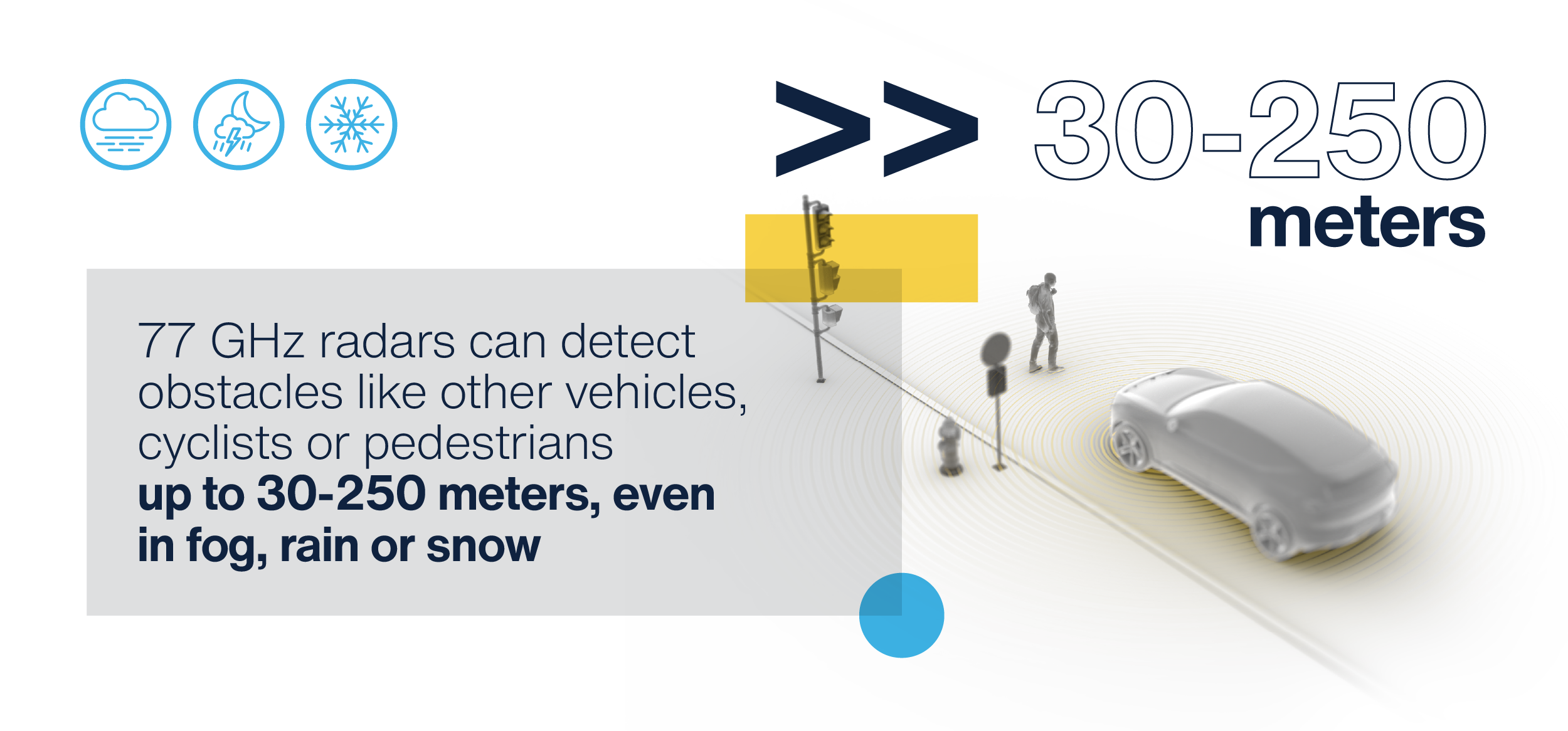
RADAR vs LiDARLet’s dive into these technologies and how they work together. Both RADAR and LiDAR enable accurate depth sensing. RADAR uses radio waves to provide long-range object detection in even the most adverse weather conditions. LiDAR emits laser light pulses to offer high precision and detail for 3D mapping. By emitting radio waves that bounce off objects and return to the sensor, RADAR systems can detect how far away an object is, the relative speed of that object, the direction of its movement and – depending on resolution and signal processing – the size and shape of that object.
With this information, vehicles are better equipped to identify potentially dangerous situations and prevent crashes. Radar technology, for example, can detect if the car in front suddenly slows down and as the gap between vehicles decreases, automatic emergency braking systems can be deployed. On a technical level, automotive radar solutions typically use 24 GHz or 77 GHz bands, balancing range and resolution requirements. While 24 GHz radars are used in Advanced Driver Assistance Systems (ADAS) to provide safety features such as blind-spot detection, rear cross traffic alerts and collision avoidance, 77 GHz radars can detect obstacles like other vehicles, cyclists or pedestrians in the 30 to 250 meter range, even in low visibility conditions like fog, rain and snow.
By comparison, LiDAR systems emit a series of short bursts of light that reflect off objects and surfaces before returning to the sensor. The “time of flight” data is used to calculate the distance to an object and create a dense collection of 3D points, mapping out a detailed 3D model. This precise object detection and classification is ideal for more complex or even semi-autonomous driving scenarios, where distinguishing between pedestrians, vehicles, and road edges is crucial. LiDAR is typically more precise than RADAR, however LiDAR is more susceptible to distortion or lower performance in fog or rainy conditions.
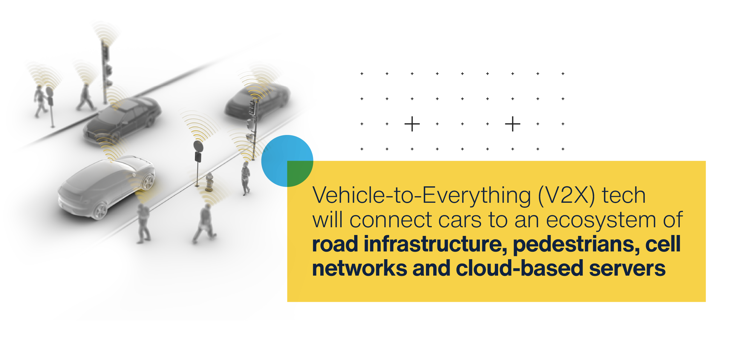
The V2X layerMany modern vehicles combine RADAR and LiDAR to formulate a more detailed and complete picture of the vehicle’s surroundings – and enables a future of Vehicle-to-Everything (V2X) communication. V2X refers to an intelligent ecosystem where cars are just one piece of the puzzle. With V2X communication, vehicles, road infrastructure, pedestrians and cellular networks or cloud-based services can exchange information in real-time.
The symbiotic relationship between these technologies is certainly exciting – with the potential to improve journeys and reduce road accidents. Environmental sensors would monitor road surface conditions. When moisture levels build up, this data can be communicated to adaptive road signs to automatically reduce speed limits. Thinking of congestion, traffic sensors can measure vehicle volumes and speeds, feeding into traffic signals so green lights can be extended when necessary to reduce traffic jams on the roads. This technology is yet to be deployed on a massive scale, but is already being tested in cities across the United States, China and Portugal – and the momentum will only increase as the benefits are felt by road users.
A connected ecosystem of carsV2X technology transforms connected cars into mobile sensors. Each car will collect anonymized data about road conditions, hazards, and traffic patterns – and also hard braking events and airbag deployments to areas of poor visibility – to benefit all road users without compromising driver privacy. In this world, authorities could apply automatic speed limitations based on real-time data from vehicle clusters – by sending a warning to the driver about a pothole, or the car auto-adjusting for those conditions.
Pedestrians would also be safer. If a vehicle’s sensors may not “see” a child on a bike about to emerge from behind a parked car, a smart roadside unit equipped with V2X technology may catch it from another vantage point to warn nearby drivers so they can slow down or even trigger automatic braking.
Data governance in the V2X ageQuestions of data privacy and accountability are also emerging as V2X capabilities continue to scale. Who is accountable if a software update introduces a safety flaw? And should anonymized safety data – from near-miss incidents to driver behavior patterns – be shared between automotive manufacturers to improve system-wide learning?
Safety improvements need to be balanced with the diminishing role of human agency in the vehicle. Though we are some years from fully autonomous vehicles, the shift is underway to reduce the margin for human error on the roads. Yet if drivers are less engaged or less able to intervene quickly if an incident arises, it could paradoxically increase risk in situations where manual override becomes necessary. The evolution of increasingly connected and autonomous vehicles must go hand-in-hand with transparency, good data stewardship, and appropriate human oversight if the industry is to build trust in a V2X-enabled future.
Driving 2.0With RADAR, LIDAR and V2X technology, vehicles are on track to become one node in a much larger and more intelligent ecosystem. They will be able to make sense of the world around them, detecting and interacting with the road, other vehicles and their wider external environment so evasive action can be taken early to avoid collisions.
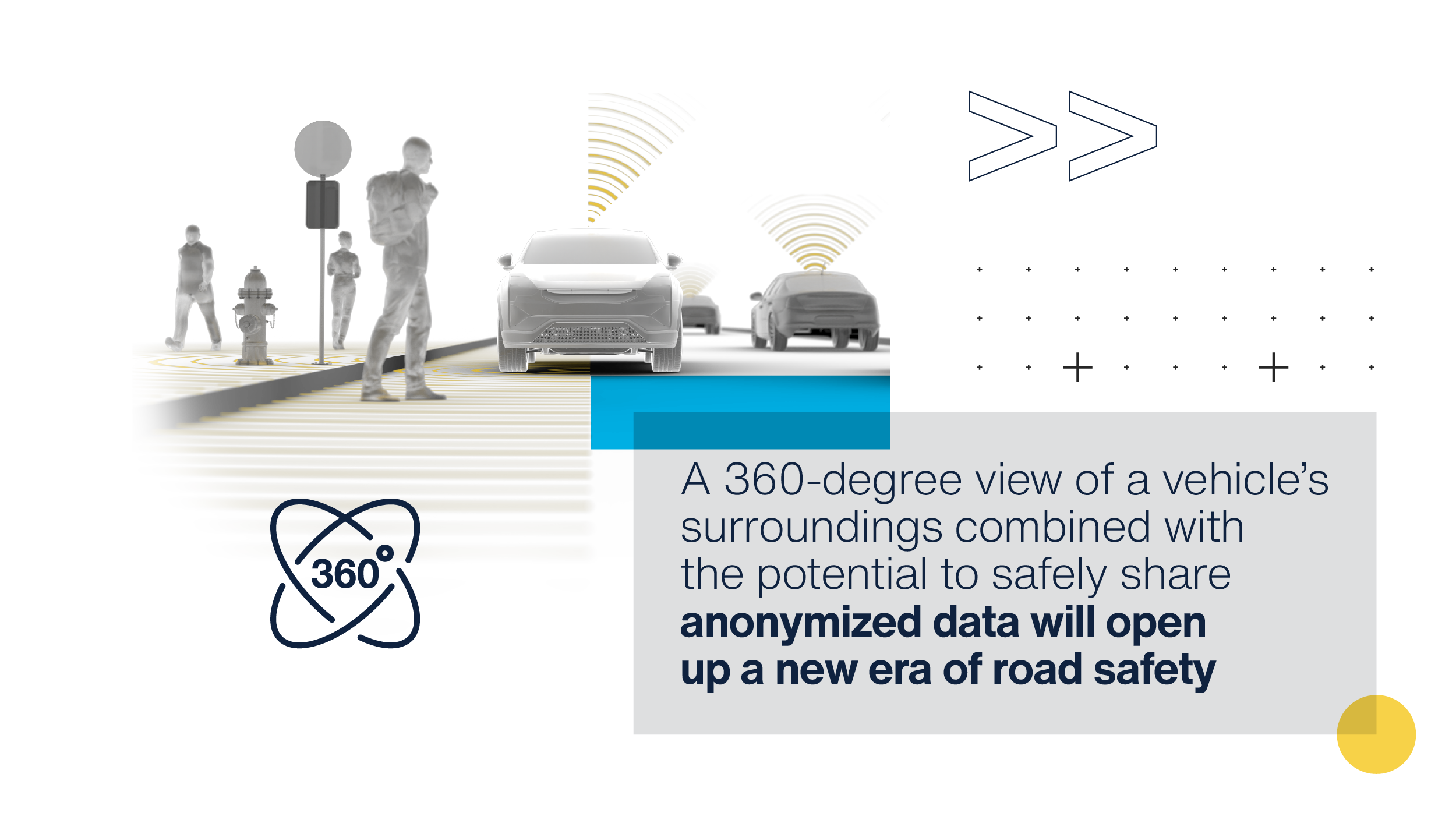
A comprehensive 360-degree view of a vehicle’s surroundings combined with the potential to safely share anonymized data will enable a new era of road safety.
The post Cars That Talk: Reimagining driving with RADAR, LIDAR and Smart Connectivity appeared first on ELE Times.
Як побудувати культуру доброчесності у ЗВО

Розбудова доброчесності в системі вищої освіти – один із пріоритетів сучасної освітньої політики України. Міністерство освіти і науки України зробило ще один важливий крок у цьому напрямі, розробивши методичні рекомендації щодо впровадження принципів доброчесності у діяльність закладів вищої освіти. Документ, затверджений наказом від 17 квітня 2025 року №576, є системним посібником для всіх, хто працює в сфері вищої освіти – від керівників і працівників адміністрацій до антикорупційних уповноважених і студентів.
Antenna Innovations Come in Sizes Ranging from a Stamp to a School Bus
Федір Тетянич. На перетині сучасного й майбутнього

Наша газета (див. "Київський полiтехнiк" № 1-2, 2024 р.) уже розповідала про мозаїчне панно "Наука", що прикрашає фасад 18-го корпусу та внесене до Переліку виявлених об'єктів культурної спадщини м. Києва. Але про його творця – художника-монументаліста Федора Тетянича (1942 – 2007) знають переважно лише фахівці. Та перший перформер незалежної України, ідеї якого випередили час і не втрачають своєї актуальності донині, не заслуговує на забуття.
Mitsubishi Electric selected for JAXA’s Space Strategy Fund to develop solar cells for Japanese satellites
Lumentum offering $1.1bn in convertible notes due in 2032
Western Australia’s Nimy appoints technical advisor on extractive metallurgy
DIY AMP board
 |
I will complete to make Input board and Vol control, LED EQ [link] [comments] |
Packing More Brains Into Buds: Multi-Feature AI on Tiny Silicon
A temperature-compensated, calibration-free anti-log amplifier
 The typical anti-log circuit
The basic anti-log amplifier looks like the familiar circuit of Figure 1.

Figure 1 The typical anti-log circuit has uncertainties related to the reverse current, Is, and is sensitive to temperature.
Wow the engineering world with your unique design: Design Ideas Submission Guide
The approximate equation for V0 given in Figure 1 comes from the Ebers-Moll model. A more advanced model employed by many modern spice simulators, such as LTspice, is the Gummel-Poon model, which I won’t discuss here. It suffices for discussions in this Design Idea (DI) to work with Ebers-Moll and to let simulations benefit from the Gummel-Poon model.
The simple Figure 1 circuit is sensitive to both temperature and the value of Is. Unfortunately, the value and limits of Is are not specified in datasheets. Interestingly, spice models employ specific parametric values for each transistor, but still say nothing about the limits of these values. Transistors taken from different sections of the same silicon wafer can have different parametric values. The differences between different wafers from the same facility can be greater yet and can be even more noticeable when those from different facilities of the same manufacturer are considered. Factor in the products of the same part number from different manufacturers, and clear, plausible concerns about design repeatability are evident.
Addressing temperature and Is variationsThere’s a need for a circuit that addresses these two banes of consistent performance. Fortunately, the circuit of Figure 2 is a known solution to the problem [1].

Figure 2 This circuit addresses variations in both temperature and Is. Key to its successful operation is that Q1a and Q1b constitute a matched pair, taken from adjacent locations on the same silicon wafer. Operating with the same VCEs is also beneficial for matching.
It works as follows. Given that Q1a and Q1b are taken from adjacent locations on the same silicon wafer, their characteristics (and specifically Is) are approximately identical (again, Is isn’t spec’d). And so, we can write that:
 It’s also clear that:

Additionally,
![]()
So:
![]()
Therefore:
![]()
Substituting Ic expressions for the two VBEs,

And here’s some of the circuit’s “magic”: whatever their value, the matched Is’s cancel! From the properties of logarithms,

Again, from the properties of logarithms:

Exponentiating, substituting for the Ic’s, and solving for V0:

Note that Vi must be negative for proper operation.
Improving temperature compensationLet’s now turn our attention to using a thermistor to deal with temperature compensation. Those I’m used to dealing with are negative temperature coefficient (NTC) devices. But they’ll do a poor job of canceling the “T” in the denominator of Equation (1). Was there an error in Reference [1]?
I exchanged the positions of R3 and the (NTC) thermistor in the circuit of Figure 2 and added a few resistors in various series and parallel combinations. Trying some resistor values, this met with some success. But the results were far better with the circuit as shown when a positive temperature coefficient (PTC) was used.
I settled on the readily available and inexpensive Vishay TFPT1206L1002FM. These are almost perfectly linear devices, especially in comparison to the highly non-linear NTCs. Figure 3 shows the differences between two such devices with resistances of 10 kΩ at 25°C. It makes sense that a properly situated nearly linear device would do a better job of canceling the linear temperature variation.

Figure 3 A comparison of a highly non-linear NTC and a nearly linear PTC.
To see if it would improve the overall temperature compensation in the Figure 2 circuit, I considered adding a fixed resistor in series with the TFPT1206L1002FM and another in parallel with that series combination.
Thinking intuitively that this three-component combination might work better in the feedback path of an inverting op amp whose input was another fixed resistor, I considered both the original non-inverting and this new inverting configurations. The question became how to find the fixed resistor values.
The argument of the exponent in Equation (1) (exclusive of Vi) provides the transfer function H(T, <resistors, PTC>), which would be ideally invariant with temperature T (with Th1 suitably modified to accommodate the series and parallel resistors).
For any given set of resistor values, the configurations apply some approximate, average attenuation α to the input voltage Vi. We need to find the values of the resistors and of α such that for each temperature Tk over a selected temperature range (I chose to work with the integer temperatures from -40°C to +85°C inclusive and used the PTC’s associated values), the following expression is minimized:

Excel’s Solver was the perfect tool for this job. (Drop me a note in this DI’s comments section if you’re interested in the details.)
The winning resultThe configurations were found to work equally well (with different value components.) I chose the inverter because it allows Vi to be a positive voltage. Figure 4 shows the winning result. The average value α was determined to be 1.1996.

Figure 4 The simulated circuit with R2a, R2b, and R3 chosen with the help of Excel’s Solver. A specific matched pair of transistors has been selected, along with values for resistors R1 and Rref, and a voltage source Vref.
For Figure 4, Equation (1) now becomes approximately:

The circuit in Figure 4 was simulated with 10° temperature steps from -40°C to +80°C and values for Vi of 100 µV, 1 mV, 10 mV, 100 mV, 1 V, and 6 V. These V0 values were divided by those given by Equation (2), which are the expected results for this circuit.
Over the industrial range of operating temperatures and more than four orders of magnitude of input voltages, Figure 5 shows a worst-case error of -4.5% / +1.0%.

Figure 5 Over the industrial range of operating temperatures and over 4.5 orders of magnitude of input voltages from 100 µV to 6 V, the Figure 4 circuit shows a worst-case error of better than -5.0% / + 1.0%. V0 ranges from 2.5 mV to 3 V.
BonusWith a minor addition, this circuit can also support a current source output. Simply split Figure 4’s R1 into two resistors in series and add the circuit of Figure 6.

Figure 6 Split R1 of Figure 4 into R1a and R1b; also add U4, Rsense, and a 2N5089 transistor to produce a current source output.
CaveatsWith all of this, the simulation does not account for variations between the IS’s of a matched pair’s transistors; I’m unaware of a source for any such information. I’ve not specified op-amps for this circuit, but they will require positive and negative supplies and should be able to swing at least 1-V negative with respect to and have a common-mode input range that includes ground. Bias currents should not exceed 10 nA, and sub-1 mV offset voltages are recommended.
Temperature compensation for anti-log ampExcel’s Solver has been used to design a temperature-compensation network for an anti-log amplifier around a nearly linear PTC thermistor. The circuit exhibits good temperature compensation over the industrial range. It operates within a signal range of more than three orders of magnitude. Voltage and current outputs are available.
References
- Jain, M. K. (n.d.). Antilog amplifiers. https://udrc.lkouniv.ac.in/Content/DepartmentContent/SM_6aac9272-bddd-4108-96ba-00a485a00155_57.pdf
Related Content
- Gain control
- Why modulate a power amplifier?—and how to do it
- Power amplifiers that oscillate—deliberately. Part 1: A simple start.
- Log and limiting amps tame rowdy communications signals
- Mutant op amp becomes instrumentation amp
The post A temperature-compensated, calibration-free anti-log amplifier appeared first on EDN.
До 100-річчя першого польоту українського пасажирського літака К-1
")
Цього літа виповнилося 100 років від першого польоту українського пасажирського літака К-1, створеного під керівництвом українського радянського авіаконструктора, випускника КПІ 1925 року Костянтина Олексійовича Калініна (1887-1938). Подія ця сталася 26 липня 1925 року.
Nagoya spinoff Photo electron Soul’s GaN-based e-beam technology targets semiconductor inspection & metrology
Tata–Merck MoU to Accelerate Chip Manufacturing Infrastructure in India
Tata Electronics Private Limited has signed a strategic Memorandum of Understanding (MoU) with Merck, a global leader in science and technology, to accelerate the development of India’s semiconductor ecosystem. The agreement, finalized, underscores a joint commitment to building robust capabilities in materials, fabrication, and supply chain infrastructure.
Under the partnership, Merck will prepare a full suite of advanced solutions for Tata Electronics, including high-purity electronic materials, advanced gas and chemical delivery systems, and turnkey fabrication infrastructure services. Merck’s AI-enhanced Material Intelligence solutions will also aid operations at Tata’s Semiconductor Fabrication Plant in Dholera, Gujarat.
The partnership encompasses more than just the transfer of technology. Merck will provide guidance on safety and production excellence practices and grant access to Athinia, a secure data analytics platform that enables collaboration at scale. The contract also foresees the establishment of local warehouses, the development of raw material supply chain, and talent development programs, all aimed at bolstering India’s position in the semiconductor sector in the world.
Tata Electronics has promised to invest ₹91,000 crore ($11 billion) in creating the Dholera semiconductor fabrication plant, the first of its kind in India. Once operational, the fab will manufacture chips for applications ranging from automotive and mobile devices to artificial intelligence and advanced computing, catering to both domestic and international markets.
This partnership is viewed as a major step in furthering the goals of the India Semiconductor Mission, establishing Merck and Tata Electronics as important figures in determining the future of high-tech production in the nation.
The post Tata–Merck MoU to Accelerate Chip Manufacturing Infrastructure in India appeared first on ELE Times.
UP Electronics Policy Draft to Boost Smartphone and Electronics Manufacturing
The Uttar Pradesh government has introduced a draft policy aimed at strengthening electronics and smartphone manufacturing in the state, with a particular focus on the Noida region. The initiative is part of the state’s broader goal of becoming a $1 trillion economy by 2030.
The draft policy titled “UP Electronics Component Manufacturing Policy 2025” has a goal of providing an ecosystem to nurture domestic and international investors. A variety of incentives, such as capital investment subsidies, stamp and electricity duty waivers, and participation interest grants are proposed to gain more participants.
The state’s IT and electronics department confirmed that the policy was approved by the cabinet in September 2025 and has been made effective retrospectively from April 1, 2025.
The policy aims to achieve $50 billion worth of electronics production within the next five years. Electronics production from U.P. is expected to grow, attracting serious investment, creating massive employment, and cementing the state’s position as a major player in India’s U.P. electronics manufacturing is expected to grow multi-fold within that period.
With Noida as a confirmed centre for electronics and smartphone production, the policy is expected to enhance the state’s role in global supply chains supporting the greater vision of India as a hub for electronics manufacturing.
The post UP Electronics Policy Draft to Boost Smartphone and Electronics Manufacturing appeared first on ELE Times.
Pages


![[link]](https://i.redd.it/ywj6pyvxezmf1.jpeg)