
Feed aggregator
Zener diode (5.1 V) voltage regulator circuit
 voltage regulator circuit") | Zener voltage = 5.1 V, Input voltage = 9 V, Resistance = 500 ohm [link] [comments] |
Nuvoton Releases Compact High-Power Violet Laser Diode (402nm, 1.7W)
Nuvoton Technology announced today the launch of its compact high-power violet laser diode (402nm, 1.7W), which achieves industry-leading optical output power in the industry-standard TO-56 CAN package. This product realizes compact size, high output power, and long-life, which were previously considered difficult, through our proprietary chip design and thermal management technologies. As a result, it contributes to space-saving and long-life optical systems for a wide range of optical applications.
Achievements:
1. Achieves industry-leading optical output power of 1.7W at 402nm in the industry-standard TO-56 CAN package, contributing to the miniaturization of optical systems.
2. Realizes long-life through proprietary chip design and thermal management technologies, reducing the running costs of optical systems.
3. Expands the lineup of mercury lamp replacement solutions, improving flexibility in product selection according to application.
Latest Addition
In addition, this product is newly added to their lineup of mercury lamp replacement solutions using semiconductor lasers, providing customers with new options. This enables flexible product selection according to application, installation environment, and required performance, improving the freedom of system design.
Its applications include:
・ Laser Direct Imaging (LDI)
・ Resin curing
・ Laser welding
・ 3D printing
・ Biomedical
・ Display
・ Alternative light source for mercury lamps, etc.
Nuvoton Technology Corporation Japan (NTCJ) joined the Nuvoton Group in 2020. As a dedicated global semiconductor manufacturer, NTCJ provides technology and various products cultivated over 60 years since its establishment, and solutions that optimally combine them. We value relationships with our customers and partners, and by providing added value that exceeds expectations, we are working as a global solution company that solves various issues in society, industry, and people’s lives.
The post Nuvoton Releases Compact High-Power Violet Laser Diode (402nm, 1.7W) appeared first on ELE Times.
Powering the Chip Chain, Part 03: “AI is Transforming the Semiconductor Value Chain End-to-End,” Says RS Components’ Amit Agnihotri
| India’s semiconductor ambitions are backed by initiatives like the ₹76,000 crore ISM and the ₹1,000 crore DLI scheme, which focuses on fostering a strong design ecosystem. A critical part of this effort is ensuring design engineers get timely access to quality components.
To highlight how distributors are enabling this, we present our exclusive series — “Powering the Chip Chain” — featuring conversations with key industry players. |
As India solidifies its position in the global electronics manufacturing landscape, the role of distribution has evolved from merely supplying components to enabling rapid, AI-driven innovation. This shift demands hyper-efficient inventory, advanced technical support, and flexible commercial policies.
In an exclusive interaction for the ‘Powering the Chip Chain’ series, Amit Agnihotri, Chief Operating Officer at RS Components & Controls (I) Ltd., shares his perspective on the exponential growth of AI-centric component demand and how digital transformation is equipping distributors to accelerate time-to-market for a new generation of Indian engineers.
AI: The New Core of Product Discovery
The integration of AI is no longer a future concept but a foundational element of distribution platforms. Mr. Agnihotri confirms that RS Components India is integrating AI into both its customer-facing systems and internal operations.
The primary objective is to make product discovery simpler, faster, and more intuitive. By leveraging AI-driven analytics, the company analyzes customer trends and buying patterns to anticipate future needs, ensuring the most relevant products are recommended with greater precision and speed. In line with this vision, RS is also investing heavily in enhancing its website recommendation engine through advanced AI, enabling customers to easily find the right products that best suit their specific applications.
“On our digital platform, AI-powered features guide users in identifying the right product based on their specific needs and selection criteria, significantly improving turnaround time and enhancing the overall experience,” says Agnihotri. This capability also extends internally, allowing RS India to optimize inventory management and ensure offerings remain aligned with volatile market demand.
Exponential Demand for Edge Intelligence
The rapid advancement of AI is fundamentally restructuring component demand, particularly accelerating the need for specialized silicon. This is most evident in the shift of high-performance components away from only high-end data centers.
Mr. Agnihotri notes that RS Components is witnessing exponential growth in AI adoption across core sectors such as automotive, electronics manufacturing, and industrial automation.
This growth is driving demand for specialized parts such as edge AI chips, neural network accelerators, and high-performance GPUs. These solutions, which support AI-centric applications across healthcare devices, autonomous systems, and smart mobility, enable customers to achieve higher processing speeds, ultra-low latency, and greater energy efficiency in their designs.
“The scale and speed at which AI technologies are being integrated into these industries indicate a clear shift in product development priorities—towards high-speed processing capabilities, ultra-low latency architectures, and energy-efficient AI hardware,” he explains.
Empowering R&D with Flexibility and Tools
To support this rapid prototyping and iteration, RS Components focuses on providing R&D teams with both technical enablement and commercial flexibility.
The support spans the entire design cycle, from concept to validation, anchored by the DesignSpark platform. This platform provides an integrated suite of free design tools, including PCB design and simulation, which accelerates the transition from concept to prototype.
Furthermore, all product listings are enriched with technical data. “All listings are enriched with datasheets, footprints, 3D models, parametric filters, and application notes so design engineers can perform compatibility checks and Design For Manufacture (DFM) assessments early in the process,” Agnihotri says.
Crucially, the company has adapted its commercial policies to match the low-volume needs of R&D work:
“Recognising that R&D and PoC work often requires small quantities of the latest components, we operate with No MOQ [Minimum Order Quantity] and No MOV [Minimum Order Value] policies on many products, and we add approximately 5,000 NPIs [New Product Introductions] to our portfolio each month.”
These practices ensure that startups, academic labs, and enterprise R&D teams can source cutting-edge parts in small batches without heavy inventory commitments.
The Policy Tailwinds and Supply Chain Agility
Government initiatives, most notably the Semicon India programme and national AI policies, are playing a material role in creating market readiness.
Amit states, “By incentivizing local manufacturing, design centers and skilling, these programs shorten lead times, attract investment and create predictable demand for AI accelerators, advanced chips and supporting components.” This policy support, he adds, allows distributors to implement deeper localization of inventory and expand value-added services.
To ensure supply chain agility in the face of this growing complexity, RS Components utilizes AI and predictive analytics. Machine-learning models ingest purchase history and market signals to produce more accurate short- and medium-term forecasts.
“AI-driven SKU segmentation and safety-stock algorithms prioritize high-demand electronic components, while predictive lead-time modelling and allocation analytics enable proactive vendor coordination,” he explains. This systemic use of AI helps manage potential foundry constraints and allocation volatility, which remains a persistent challenge in the global semiconductor ecosystem.
Conclusion: The Distributor as an Innovation Partner
Mr. Agnihotri concludes by emphasizing that AI will continue to transform the semiconductor value chain end-to-end—from component design (using AI for simulation) to distribution (through predictive analytics and personalized recommendations).
RS Components’ strategy is clear: by embedding AI into its DesignSpark toolchain, leveraging predictive models to localize inventory, and providing flexible commercial terms, the company is positioning itself as a strategic partner. This integrated approach enables engineers and manufacturers to iterate quickly, source the right components, and scale with confidence, fundamentally accelerating innovation across the Indian market.
The post Powering the Chip Chain, Part 03: “AI is Transforming the Semiconductor Value Chain End-to-End,” Says RS Components’ Amit Agnihotri appeared first on ELE Times.
Екскурсія до R&D центру компанії ТОВ "ПлазмаТек"

Спочатку було слово – оголошення на сторінці профбюро студентів НН ІМЗ (https://t.me/pbikpiii/1) з перепостом на сторінці студентського профкому КПІ (https://t.me/pskpi) про те, що профспілкова організація Інституту запрошує студентів усіх факультетів 7 листопада взяти участь в екскурсії до R&D центру (Центру досліджень і розробок) компанії ТОВ "ПлазмаТек".
Avicena’s LightBundle optical links operating at 4Gbps per lane with transmitter current as low as 100µA per LED
A budget battery charger that also elevates blood pressure

At the tail end of my September 1 teardown of EBL’s first-generation 8-bay battery charger:

I tacked on a one-paragraph confession, with an accompanying photo that as usual, included a 0.75″ (19.1 mm) diameter U.S. penny for size comparison purposes:
I’ll wrap up with a teaser photo of another, smaller, but no less finicky battery charger that I’ve also taken apart, but, due to this piece as-is ending up longer-than-expected (what else is new?), I have decided to instead save for another dedicated teardown writeup for another day:

That day is today. And by “finicky”, as was the case with its predecessor, I was referring to its penchant for “rejecting batteries that other chargers accepted complaint-free.”

Truth be told, I can’t recall how it came into my possession in the first place, nor how long I’ve owned it (aside from a nebulous “really long time”). Whatever semblance of an owner’s manual originally came with the charger is also long gone; tedious searches of both my file cabinet and online resources were fruitless. There’s not even a company name or product code to be found anywhere on the outer device labeling, just a vague “Smart Timer Charger” moniker:


The best I’ve been able to do, thanks to Google Image Search, is come across similar-looking device matches from a company called “Vidpro Power2000” (with the second word variously alternatively referred to as “Power 2000”) listed on Amazon under multiple different product names, such as the XP-333 when bundled with four 2900 mah AA NiMH batteries:

and the XP-350 with four accompanying 1000mAh AAA batteries, again NiMH-based:

My guess is that neither “Vidpro Power2000” nor whatever retail brand name was associated with this particular charger was actually the original manufacturer. And by the way, those three plastic “bumps” toward the top of the front panel, above the battery compartment and below the “Power2000” mark, aren’t functional, only cosmetic. The only two active LEDs are the rectangular ones at the front panel’s bottom edge, seen in action in an earlier photo.
Anyhoo, after some preparatory top, bottom, and side chassis views as supplements to the already shared front and back perspectives:


Let’s work our way inside, beginning (and ending?) with the visible screw head in between the two foldable AC plug prongs:


Nope, that wasn’t enough:

Wonder what, if anything, is under the back panel sticker? A-ha:


There we are:


“Nice” unsightly blob of dried glue in the upper left corner there, eh?

No more screws, clips, or other retainers left; the PCB lifts away from the remainder of the plastic chassis straightaway:

As I noted earlier, those “three bumps” are completely cosmetic, with no functional purpose:

And speaking of cosmetics, the two-tone two-sided PCB is an unexpected aesthetic bonus:

As you may have already noticed from the earlier glimpse of the PCB’s backside, the trace regions are sizeable, befitting their hefty AC and DC power routing purposes and akin to those seen last time (where, come to think of it, the PCB was also two-tone for the two sides). But the PCB itself is elementary, seemingly with no embedded trace layers, therein explaining the between-regions routing jumpers that through-hole feed to the other side:

We’ve also finally found a product name: the “TL2000S” from “Samyatech”. My Google search results on the product code were fruitless; let me know in the comments if you had any better luck (I’m particularly interested in finding a PDF’d user manual). My research on the company was more fruitful, but only barely so. There are (or perhaps more accurately in this case, were) two companies that use(d) the “Samyatech” abbreviation, both named “Samya Technology” in full. One is based in Taiwan, the other is in South Korea. The former, I’m guessing, is our candidate:
Samya Technology is a manufacturer of charging solutions for consumer products. The company manufactures power banks, emergency chargers, mobile phone battery chargers, USB charging products, Solar based chargers, Secondary NiMH Batteries, Multifunction chargers, etc. The company has two production bases, one in Taiwan and the other in China.
The website associated with the main company URL, www.samyatech.com, is currently timing out for me. Internet Archive Wayback Machine snapshots suggest two more information bits:
- The main URL used to redirect to samyatech.com.tw, which is also timing out, and
- More generally, although I can’t read Chinese, so don’t take what I’m saying as “gospel”, it seems the company shut down at the start of the COVID-19 lockdown and didn’t reopen.
Up top is the AC-to-DC conversion circuitry, along with other passives:

And at the bottom are the aforementioned LEDs and their attached light pipes:

Back to the PCB backside, this time freed of its previous surrounding-chassis encumbrance:

That blotch of dried glue sure is ugly (not to mention, unlike its same-color counterparts on the other side that keep various components in place, of no obvious functional value), isn’t it?

The IC nexus of the design was a surprise (at least to me, perhaps less so to others who are already more immersed in the details of such designs):

At left is the AZ324M, a quad low-power op amp device from (judging by the company logo mark) Advanced Analog Circuits, part of BCD Semiconductor Manufacturing Limited, and subsequently acquired by Diodes Incorporated.
And at right? When I first saw the distinctive STMicroelectronics mark on one end of the package topside, I assumed I was dealing with a low-end firmware-fueled microcontroller. But I was wrong. It’s the HCF4060, a 14-stage ripple carry binary counter/divider and oscillator. As the Build Electronics Circuits website notes, “It can be used to produce selectable time delays or to create signals of different frequencies.”
This all ties to, as I’ve been able to gather from my admittedly limited knowledge and research, how basic battery chargers like this one work in the first place (along with why they tend to be so fickle). Perhaps obviously, it’s important upfront for such a charger to be able to discern whether the batteries installed in it are actually the intended rechargeable NiMH formulation.
So, it first subjects the cells to a short-duration, relatively high current pulse (referencing the HCF4060’s time delay function), then reads back their voltages. If it discerns that a cell has a higher-than-expected resistance, it assumes that this battery’s not rechargeable or is instead based on an alternative chemistry such as alkaline or NiCd…and terminates the charge cycle.
That said, rechargeable NiMH cells’ internal resistance also tends to increase with use and incremental recharge cycles. And batteries that are in an over-discharge state, whether from sitting around unused (a particular problem with early cells that weren’t based on low self-discharge architectures) or from being excessively drained by whatever device they were installed in, tend to be intolerant of elementary recharging algorithms, too.
That said, I’ve conversely in the past sometimes been able to convince this charger to accept a cell that it initially rejected, even if the battery was already “full” (if I’ve lost premises power and the charger acts flaky when the electricity subsequently starts flowing again later, for example) by popping it into an illuminated flashlight for a few minutes to drain off some of the stored electrons.
So… And again, as I mentioned back in September, a more “intelligent” (albeit also more expensive) charger such as my La Crosse Technology BC-9009 AlphaPower is commonly much more copacetic with (including being capable of resurrecting) cells that simplistic chargers comparatively reject:

Some side-view shots in closing, including closeups:


And with that, I’ll turn it over to you for your thoughts in the comments. A reminder that I’m only nominally cognizant of analog and power topics (and truth be told, I’m probably being overly generous-of-self in even claiming that), dear readers—I’m much more of a “digital guy”—so tact in your responses is as-always appreciated! I’m also curious to poll your opinions as to whether I should bother putting the charger back together and donating it to another, as I normally do with devices I non-destructively tear down, or if it’d be better in this case to save potential recipients the hassle and instead destine it for the landfill. Let me know!
—Brian Dipert is the Principal at Sierra Media and a former technical editor at EDN Magazine, where he still regularly contributes as a freelancer.
Related Content
- Tearing apart a multi-battery charger
- Resurrecting a 6-amp battery charger
- Tricky 12V Battery Charger Circuit
- Simplifying multichemistry-battery chargers
- 12V Battery Charger Circuit using SCR
The post A budget battery charger that also elevates blood pressure appeared first on EDN.
Enhancing Embedded Systems with Automation using CI/CD and Circuit Isolation Techniques
Courtesy: Lokesh Kumar, Staff Engineer, STMicroelectronics and Raunaque Mujeeb QUAISER, Group Manager, STMicroelectronics
To keep pace with constantly advancing technological ecosystems, automation has become a focus area for innovation, efficiency and delivering quality results. One of the significant areas where automation is making impact is in embedded systems.
Embedded systems are characterized by their ability to operate with minimal human intervention, often in real-time, and are integral to the functionality of many devices we rely on daily. The integration of automation into these systems is changing the way they are designed, developed, and deployed, leading to enhanced performance, reliability, and scalability.
Current challenges of automation
A typical embedded system development platform includes multiple jumpers, switches, and buttons for enabling various hardware (HW) configurations like boot modes, programming mode or enabling different HW features. Due to this it becomes difficult to automate and truly validate embedded board and software for all HW configurations remotely or via automation.
While this can be solved using mechanical arms and similar concepts, it is very costly and not time efficient, hence making it not practically a feasible solution. Another alternate solution is using development boards, but it deviates from actual testing scenario.
Proposed Solution:
We will explore the use of circuit isolation techniques and the adoption of the Jenkins ecosystem for continuous integration and continuous deployment (CI/CD). Circuit isolation ensures that test controller can configure the embedded systems under test safely and reliably by preventing electrical faults and interference from affecting the system’s performance while Jenkins provide a robust framework for automating the software development lifecycle of embedded systems. Jenkins, an open-source automation server, enables developers to build, test, and deploy code efficiently and consistently. By integrating Jenkins with embedded system development, teams can achieve faster iteration cycles, improved code quality, and seamless deployment processes.
The proposed solution shares a cost-effective solution with easy to implement method to overcome above mentioned limitations.
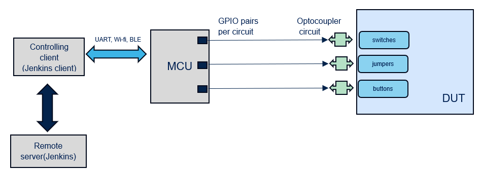 Figure 1: Block diagram of Test Automation Setup
Figure 1 shows the block diagram of automation architecture where a small footprint microcontroller can be used to control an isolation circuit connected to the junctions of switch/jumper/buttons of embedded device under test (DUT). Isolation circuit (e.g., Optocoupler) ensures circuit safety. In the current demonstration NUCLEO-F401RE board (MCU) is used to control the optocoupler circuit connected to boot modes switches and reset button of STM32MP157F-DK2 board under test (DUT). Jenkins will issue remote commands to MCU.
 Figure 2 : Circuit Diagram for controlling HW configurations
Figure 2 demonstrates the circuit diagram where MCU can control the state of two-way Switch SW1. VDD is connected to one end of output and R1 register is added to limit current. The value of R1 is based on the embedded device specification. In the default state, the physical switch is put in off state. Then depending on which boot combination we want, MCU will enable the output side of Optocoupler circuit.
For example, to put STM32MP157F-DK2 in SD card mode, GPIO pair 1 and GPIO pair 2 will be put in HIGH state. This will short output circuit and achieve 1,0,1 combination for SD card boot configuration. A similar circuit is present at the embedded device Reset button. After changing configuration, one can trigger reset to boot in desired hardware configuration.
Jenkins is used to remotely send commands to NUCLEO-F401RE board through a computer containing automation scripts (python and shell scripts) which translates commands to configurations and sends it to MCU to change the device under test (DUT) state as explained above. Using this setup, one can manage all HW configurations remotely. The above arrangement successfully enables the developer to remotely perform board programming / flashing, toggling boot switches and configurations on STM32MP157F-DK2.
 Figure 3: Jenkins pipeline example
Python scripts are present on PC (Jenkins client) controlling MCU and Jenkins is used to invoke these scripts via Jenkins pipeline/scripts.
Scope and Advantages
The proposed solution can be extended to various embedded boards due to the small circuit size that can be easily connected to DUT. Also, a single MCU can control multiple circuits depending on the count of the GPIOs available on a given, multiple DUTs can be controlled. Another advantage being the low cost of circuits and MCU’s and solution is flexible due to multiple options being available to control it (UART, Bluetooth, I2C, SPI, Wi-Fi). Although the solution needs one controlling client which is used to control the Automation system remotely, one client can be used to control multiple Automation systems and thus making the solution scalable and reliable in every aspect as hardware configurations are also tested.
Future work:
Embedded systems can include pin connections at desired switches and buttons, then the need for soldering is eliminated and one can simply connect MCU and isolation circuit to achieve complete and reliable automation.
The post Enhancing Embedded Systems with Automation using CI/CD and Circuit Isolation Techniques appeared first on ELE Times.
Cabinet approves Rare Earth Permanent Magnet Manufacturing Scheme, worth Rs. 7,280 crores
The Cabinet approved the Rs. 7,280 crore Rare Earth Permanent Manufacturing Scheme on November 26, Wednesday. This first-of-its kind initiative aims to establish a six thousand metric tonnes per annum of integrated Rare Earth Permanent Magnet manufacturing in the country.
Cabinet Minister Ashwini Vaishnav, highlighted the importance of Earth Permanent Magnets for electric vehicles, renewable energy, electronics, aerospace, and defence applications at a media briefing in New Delhi. The scheme is expected to support the creation of integrated manufacturing facilities, involving conversion of rare earth oxides to metals, metals to alloys, and alloys to finished Rare Earth Permanent Magnet, the Union Minister added.
As the demand for electric vehicles grows, the demand for permanent magnets is expected to double by 2030. Currently India primarily relies on imports to satisfy its requirements for permanent magnets. This new scheme is expected to play a significant role in generating employment, boosting self-reliance, and accelerating the country’s aim to achieve Net Zero by 2070.
The total duration of the scheme will be seven years from the date of award, including a two-year gestation period for setting up an integrated Rare Earth Permanent Magnet manufacturing facility. The scheme envisions allocating the total capacity to five beneficiaries through a global competitive bidding process.
The post Cabinet approves Rare Earth Permanent Magnet Manufacturing Scheme, worth Rs. 7,280 crores appeared first on ELE Times.
Decoding the Future of Electronics with TI India
In an exclusive conversation with Kumar Harshit, Technology Correspondent, ELE Times, Mr. Kumar details how TI is leading the charge in creating a safer, greener, and smarter world through technology contributions from right here in India and shares his perspective on the future skill sets required for electronics engineers to thrive in the age of artificial intelligence.
Santhosh Kumar, President & Managing Director of Texas Instruments India, discusses the core themes of safety, sustainability, and innovation and outlines the transformative role of AI in shaping the next generation of engineering talent.
Here are the excerpts from the conversation:
ELE TIMES: Given the increasing focus on road safety, particularly for two-wheelers, how is TI leveraging technology to create safer and smarter vehicles?
Santhosh Kumar: Two-wheeler safety is critical, as the rider is the most exposed. We focus on leveraging simple, easy-to-deploy sensing technologies to solve real-world problems. For example, ensuring the side stand is retracted before the vehicle moves is a simple technique, often solved with magnetic sensing connected directly to the engine control. Moving to more advanced safety, we utilize radar and multiple sensors to provide warnings for both sides of the road. We also integrate technology that can help slow or stop a vehicle automatically if the car in front suddenly brakes, even if the rider isn’t fully alert. The goal is to either give the vehicle control to avoid a fatal accident or empower the rider with timely warnings.
ELE Times: TI emphasizes collaboration and community-driven innovation. How important are industry events like Electronica in deepening your relationship with the engineering ecosystem?
Santhosh Kumar: These events are vital for two key interactions. First, our engineers love to work directly with the engineers of our customers. This technical bond is the strongest foundation for creating relevant products. Events like this provide an apt platform for us to build and deepen those relationships. Second, we connect with decision-makers and purchase teams to demonstrate the affordability and worthiness of a product as a feature for mass-market products. Ultimately, innovation doesn’t happen in isolation; it comes from interaction within a community and ecosystem, making these floors essential.
ELE Times: The world is demanding greener technology. Could you outline TI’s commitment to sustainability, both in terms of internal operations and product design?
Santhosh Kumar: We are sensitive to the work we do both inside and outside our factories. Internally, we have a goal to be 100% powered by green energy by 2030, and we are well past 30% today. Furthermore, over 90% of our operational waste is diverted from landfills.
From a product design perspective, we are very sensitive to ensuring our products take up the smallest area and consume the least amount of power. We are always optimizing to create the smallest possible MCU with minimal energy consumption. This approach allows our customers to create products that are inherently greener than they would otherwise have been.
ELE Times: Can you introduce us to TI’s innovative product line in the Power management area?
Santhosh Kumar: We are heavily focused on smart, intelligent systems. A prime example is our Battery Management Systems (BMS), designed and developed in collaboration with engineers in India, ensuring power is used exactly as intended. We have several compelling demos on motor control. India has billions of motors running today, and we are showing how to make them run most efficiently, with the lowest possible cost, without sound, and without losses. You can witness these technologies integrated, such as in our two-wheeler demonstration, combining BMS, motor control, and security features. Given the huge push towards industrial and factory automation in India, we are also showcasing numerous technologies adapted for smarter, more secure, and greener appliances for the 1.4 billion people consuming electricity.
ELE Times: Beyond the automotive and industrial sectors, what are the emerging market segments in India that you see offering significant opportunities for TI’s growth?
Santhosh Kumar: We operate across five core segments, and we see growth in all of them. After automotive and broad industrial (which includes medical electronics, where a lot of Indian innovation is happening), the third key segment is personal electronics. This includes audio, video, and speech, where AI is bringing about a tremendous influx of smarter systems. The large bandwidth and data flow driving these first three segments necessitate our involvement in the communication segment, which forms the backbone. Finally, the enterprise business is the fifth segment. We are seeing customers, product creators, and applications happening in all five areas across India.
ELE Times: Texas Instruments India has been a pioneer for over 40 years. Could you detail the strategic role TIPL plays in driving cutting-edge innovation for TI’s global business units?
Santhosh Kumar: TI India is an important entity to our worldwide business. We have architects, product definers, system engineers, analog and RF designers, and application engineers who manage businesses and contribute to the entire value chain. In fact, many TI’s new products today have a significant contribution from India, including end-to-end product development. We have world-class infrastructure, including labs, benches, and all the necessary equipment in Bangalore, to enable us to contribute to the success of these global products.
ELE Times: Can you share a recent technological breakthrough from TI and define what innovation means to Texas Instruments in the context of solving real-world problems?
Santhosh Kumar: A recent breakthrough we are very excited about is our Gallium Nitride (GaN) solutions. For instance, deploying GaN in two-wheeler chargers can shrink their size by one-third compared to existing technology and significantly reduce power consumption and heat generation due to lower leakage.
To us, innovation extends beyond laboratory research; it is about how we look at real-world problems and use technology to solve them, ultimately enhancing people’s quality of life. We have both an opportunity and a responsibility to improve the lives of eight billion people while preserving the planet.
ELE Times: Talent acquisition is key to sustained innovation. What initiatives does TI India have in place to attract and nurture the next generation of core engineering talent?
Santhosh Kumar: Our strategy is to hire the bright talent directly from campuses, which accounts for 80% of our hiring. To feed this pipeline, we have programs like our Women in Semiconductor and Hardware (WiSH) program, which engages female students beginning in their second year of college. This program provides hands-on experience in core engineering disciplines, including design, testing, verification, and validation. We want to allow a large segment of the population to understand what it means to do core engineering and be a part of world-class product development right here in India.
ELE Times: As a leader who has seen India’s electronics landscape evolve over decades, what is your key message for the industry today?
Santhosh Kumar: The key message is to adopt the technologies happening globally and bring in innovation through new products. This is a tremendous opportunity for India to lead the wave of innovation, to solve real-world problems. We can bring innovation in manufacturing, product development, and applications that lift the quality of life for our people here and for the eight billion people worldwide. With the current energy in the ecosystem and the influx of new players, India can play an important role in driving innovation.
The post Decoding the Future of Electronics with TI India appeared first on ELE Times.
Підземні сховища з ґрунтобетону: надійні, дешеві, швидкі у зведенні

На конкурсі інноваційних проєктів у межах фестивалю "Sikorsky Challenge 2025", що нещодавно пройшов у КПІ, визначили переможців, які отримають фінансування на реалізацію своїх ідей. Це вже четвертий фестиваль, проведений в умовах війни, тож серед його пріоритетів був оборонний форум, а також проєкти, спрямовані на захист цивільного населення та критичної інфраструктури. Про одну з розробок, що стосується нагальної потреби – побудови укриттів, розповідають її автори.
Delta-sigma demystified: Basics behind high-precision conversion

Delta-sigma (ΔΣ) converters may sound complex, but at their core, they are all about precision. In this post, we will peel back the layers and uncover the fundamentals behind their elegant design.
At the heart of many precision measurement systems lies the delta-sigma converter, an architecture engineered for accuracy. By trading speed for resolution, it excels in low-frequency applications where precision matters most, including instrumentation, audio, and industrial sensing. And it’s worth noting that delta-sigma and sigma-delta are interchangeable terms for the same signal conversion architecture.
Sigma-delta classic: The enduring AD7701
Let us begin with a nod to the venerable AD7701, a 16-bit sigma-delta ADC that sets a high bar for precision conversion. At its core, the device employs a continuous-time analog modulator whose average output duty cycle tracks the input signal. This modulated stream feeds a six-pole Gaussian digital filter, delivering 16-bit updates to the output register at rates up to 4 kHz.
Timing parameters—including sampling rate, filter corner, and output word rate—are governed by a master clock, sourced either externally or via an on-chip crystal oscillator. The converter’s linearity is inherently robust, and its self-calibration engine ensures endpoint accuracy by adjusting zero and full-scale references on demand. This calibration can also be extended to compensate for system-level offset and gain errors.
Data access is handled through a flexible serial interface supporting asynchronous UART-compatible mode and two synchronous modes for seamless integration with shift registers or standard microcontroller serial ports.
Introduced in the early 1990s, Analog Devices’ AD7701 helped pioneer low-power, high-resolution sigma-delta conversion for instrumentation and industrial sensing. While newer ADCs have since expanded on their capabilities, AD7701 remains in production and continues to serve in legacy systems and precision applications where its simplicity and reliability still resonate.
The following figure illustrates the functional block diagram of this enduring 16-bit sigma-delta ADC.

Figure 1 Functional block diagram of AD7701 showcases its key architectural elements. Source: Analog Devices Inc.
Delta-sigma ADCs and DACs
Delta-sigma converters—both analog-to-digital converters (ADCs) and digital-to-analog converters (DACs)—leverage oversampling and noise shaping to achieve high-resolution signal conversion with relatively simple analog circuitry.
In a delta-sigma ADC, the input signal is sampled at a much higher rate than the Nyquist frequency and passed through a modulator that emphasizes quantization noise at higher frequencies. A digital filter then removes this noise and decimates the signal to the desired resolution.
Conversely, delta-sigma DACs take high-resolution digital data, shape the noise spectrum, and output a high-rate bitstream that is smoothed by an analog low-pass filter. This architecture excels in audio and precision measurement applications due to its ability to deliver robust linearity and dynamic range with minimal analog complexity.
Note that from here onward, the focus is exclusively on delta-sigma ADCs. While DACs share similar architectural elements, their operational context and signal flow differ significantly. To maintain clarity and relevance, DACs are omitted from this discussion—perhaps a topic for a future segment.
Inside the delta-sigma ADC
A delta-sigma ADC typically consists of two core elements: a delta-sigma modulator, which generates a high-speed bitstream, and a low-pass filter that extracts the usable signal. The modulator outputs a one-bit serial stream at a rate far exceeding the converter’s data rate.
To recover the average signal level encoded in this stream, a low-pass filter is essential; it suppresses high-frequency quantization noise and reveals the underlying low-frequency content. At the heart of every delta-sigma ADC lies the modulator itself; its output bitstream represents input signal’s amplitude through its average value.
A block diagram of a simple analog first-order delta-sigma modulator is shown below.

Figure 2 The block diagram of a simple analog first-order delta-sigma modulator illustrates its core components. Source: Author
This modulator operates through a negative feedback loop composed of an integrator, a comparator, and a 1-bit DAC. The integrator accumulates the difference between the input signal and the DAC’s output. The comparator then evaluates this integrated signal against a reference voltage, producing a 1-bit data stream. This stream is fed back through DAC, closing the loop and enabling continuous refinement of the output.
Following the delta-sigma modulator, the 1-bit data stream undergoes decimation via a digital filter (decimation filter). This process involves data averaging and sample rate reduction, yielding a multi-bit digital output. Decimation concentrates the signal’s relevant information into a narrower bandwidth, enhancing resolution while suppressing quantization noise within the band of interest.
It’s no secret to most engineers that second-order delta-sigma ADCs push noise shaping further by using two integrators in the modulator loop. This deeper shaping shifts quantization noise farther into high frequencies, improving in-band resolution at a given oversampling ratio.
While the design adds complexity, it enhances signal fidelity and eases post-filtering demands. Second-order modulators are common in precision applications like audio and instrumentation, though stability and loop tuning become more critical as order increases.
Well, at its core, the delta-sigma ADC represents a seamless integration of analog and digital processing. Its ability to achieve high-resolution conversion stems from the coordinated use of oversampling, noise shaping, and decimation—striking a delicate balance between speed and precision.
Delta-sigma ADCs made approachable
Although delta-sigma conversion is a complex process, several prewired ADC modules—built around popular, low-cost ICs like the HX711, ADS1232/34, and CS1237/38—make experimentation remarkably accessible. These chips offer high-resolution conversion with minimal external components, ideal for precision sensing and weighing applications.

Figure 3 A few widely used modules simplify delta-sigma ADC practice, even for those just starting out. Source: Author
Delta-sigma vs. flash ADCs vs. SAR
Most of you already know this, but flash ADCs are the speed demons of the converter world—using parallel comparators to achieve ultra-fast conversion, typically at the expense of resolution.
Flash ADCs and delta-sigma architectures serve distinct roles, with conversion rates differing by up to two orders of magnitude. Delta-sigma ADCs are ideal for low-bandwidth applications—typically below 1 MHz—where high resolution (12 to 24 bits) is required. Their oversampling approach trades speed for precision, followed by filtering to suppress quantization noise. This also simplifies anti-aliasing requirements.
While delta-sigma ADCs excel in resolution, they are less efficient for multichannel systems. Architecture may use sampled-data modulators or continuous-time filters. The latter shows promise for higher conversion rates—potentially reaching hundreds of Msps—but with lower resolution (6 to 8 bits). Still in early R&D, continuous-time delta-sigma designs may challenge flash ADCs in mid-speed applications.
Interestingly, flash ADCs can also serve as internal building blocks within delta-sigma circuits to boost conversion rates.
Also, successive approximation register (SAR) ADCs sit comfortably between flash and delta-sigma designs, offering a practical blend of speed, resolution, and efficiency. Unlike flash ADCs, which prioritize raw speed using parallel comparators, SAR converters use a binary search approach that is slower but far more power-efficient.
Compared to delta-sigma ADCs, SAR designs avoid oversampling and complex filtering, making them ideal for moderate-resolution, real-time applications. Each architecture has its sweet spot: flash for ultra-fast, low-resolution tasks; delta-sigma for high-precision, low-bandwidth needs; and SAR for balanced performance across a wide range of embedded systems.
Delta-sigma converters elegantly bridge the analog and digital worlds, offering high-resolution performance through clever noise shaping and oversampling. Whether you are designing precision instrumentation or exploring audio fidelity, understanding their principles unlocks a deeper appreciation for modern signal processing.
Curious how these concepts translate into real-world design choices? Join the conversation—share your favorite delta-sigma use case or challenge in the comments. Let us map the noise floor together and surface the insights that matter.
 T.K. Hareendran is a self-taught electronics enthusiast with a strong passion for innovative circuit design and hands-on technology. He develops both experimental and practical electronic projects, documenting and sharing his work to support fellow tinkerers and learners. Beyond the workbench, he dedicates time to technical writing and hardware evaluations to contribute meaningfully to the maker community.
Related Content
- Delta-sigma ADCs in a nutshell
- Delta-sigma ADC basics: How the digital filter works
- Recent Developments for SAR and Sigma Delta ADCs
- Understanding sigma delta ADCs: A non-mathematical approach
- 24-Bit, 16-Channel Delta-Sigma ADC Simplifies Front-End Signal Conditioning
The post Delta-sigma demystified: Basics behind high-precision conversion appeared first on EDN.
What you see here was way ahead of its time
 | Late 90s before Ethernet control was anywhere near affordable and circuit control over the Internet was sci-fi dreams here was a $20 external HP JetDirect print sever controlling 8 GPIOs with Opto22 SSRs and a little fool logic to make the print sever think its connected to a real printer lol the NAND gate fooled the JetDirect that every time a byte was "sent to the printer" the printer flapped strobe as if it has printed the bye :) Data was piped via good old Linux NetCat - wait using Linux in the 90s...oh I'm getting emotional already I’ve so forgotten those days of badass innovation - now smart plugs are everywhere … [link] [comments] |
This looks like a very interesting Xbox controller I found
 | Sorry for light getting in the way of appreciating the full beauty of this PCB :)) [link] [comments] |
Weekly discussion, complaint, and rant thread
Open to anything, including discussions, complaints, and rants.
Sub rules do not apply, so don't bother reporting incivility, off-topic, or spam.
Reddit-wide rules do apply.
To see the newest posts, sort the comments by "new" (instead of "best" or "top").
[link] [comments]
🔥 Онлайн-лекторій «Доброчесність та антикорупція: свідомість, відповідальність, приклад»

Хочете дізнатися, як штучний інтелект викриває корупцію? Або як доброчесність може стати вашою кар’єрною суперсилою? Тоді ви точно не можете пропустити наш онлайн-лекторій «Доброчесність та антикорупція: свідомість, відповідальність, приклад», який відбудеться у межах Тижня доброчесності🔥
Old Apple IIgs Monitor LED module.
 | Wish I had a spec sheet on this part. This was pulled from an Apple IIgs monitor. I don't think it's a true led. Works lovely on 5v [link] [comments] |
The SN76477 Demo Circuit
The SN76477 "Demo Circuit":
This is a 1977 Complex Sound Generator chip from Texas Instruments. Like a lot of nerds, I got one from Radio Shack, put it in an experimenter's plugboard and got various airplane, gunshot and "ray gun" noises out of it.
In the datasheet, there was one more schematic that sat in the back of my brain for these decades; the "Demo circuit".
Over time, you learn that a schematic is a fraction of what you need to build a circuit. The chip is the biggest thing in the drawing and if you're young, you think that if you've got this IC, your nearly at home plate. This schematic (there are several iterations from the past fifty-odd years) has many rotary switches, potentiometers, capacitors and resistors. There's a 7805 regulator and two jacks, but a lot is missing; there are "R-xx" numbers for the resistors and pots, but no "C-xx" numbers for the caps. J1 and J2 are unlabeled; most of the controls are unlabeled. This being a sound project, I think it's a big deal that none of the pots are noted as being linear or audio taper. On some of the drawings, two capacitors on SW7 are swapped; it would work but it'd feel flaky as you turned the switch and listened to the result
My question a couple of months ago was, "Has anybody actually built this thing?"
It appears that the answer is "No".
I spent some time with Digi-Key's web site, Excel for pricing and Visio to lay out knobs, switches and labels.
I didn't count buying two of each potentiometer, one audio taper and one linear.
I didn't count cabinet parts; the Visio work was to find the size of the front panel. The layout isn't anything like how a real build would be done; the jacks are together, the toggle switches are together, etc.
I also have never seen a 9/16" punch that leaves a tab to keep the switch from spinning in it's hole; I know they existed but I think someone cast them into the sun before the Internet got invented.
So parts would be something over $250.00 without a cabinet; the panel would be about 18" square. A 19" wide rack panel, 10U tall would do it, and you'd want it in a console of some kind, which seems expensive to think about unless you made it out of wood, and it's still designed to be powered by a 9-volt battery; the entire project feels like a collision between the cheap and the expensive.
A quick search of Reddit and/or YouTube finds a box made with less knobs and no labelling, making sounds that scream "1977 science fiction", and not Star Wars. More like that show where Jim Nabors and Ruby Buzzi played two robots.
Letting go of the Demo Circuit, another drawing in the datasheet is a block diagram of the circuit. Most of the building blocks were in big Moog and other synthesizers in the late 1960's through late 1980's; tiny parts of Keith Emerson's rig or the stuff a guy called "Tomita" used. I don't have the space or musical talent for such a thing, but I wondered about emulators, then of course Free emulators.
I ended up at https://vcvrack.com/ , download the free version, and in less than 30 minutes had an emulated SN76477 running on my computer.
I could've probably added a MIDI tracker and had it play music. If you have a MIDI keyboard, you might be able to try the "organ" project in the datasheets.
If you had budget, time, determination, space and both electronic and musical talent, you could build the Demo Circuit, and you'd probably want to somehow interface it with a keyboard. I could see somebody like David Guetta or Deadmau5 have this on one far side of the stage and do something silly as a break between the regular show, but I don't think that it could make such awesome sounds that the great orchestras would retire in shame.
That's what I figured out about the SN76477 this fall.
Regards, Mark Stout
[link] [comments]
Making this for my esp32 p4 FBDCDC and ENDCDC pins, hope it's helpful
 | submitted by /u/PepeIsLife69_ [link] [comments] |
SemiLEDs full-year revenue grows eight-fold, despite last-quarter drop
4 bit full Adder
 | I've assembled this 4 bit full adder with logic ics. [link] [comments] |
Pages


![[link]](https://i.redd.it/hzq3plrtgq4g1.jpeg)
![[link]](https://i.redd.it/p2ljck8hx14g1.png)
![[link]](https://i.redd.it/bxwn87u6j04g1.jpeg)