
Feed aggregator
Slim DIN Rail Power Supplies For Industrial Applications
Advertorial by RECOM
DIN rail mounting has revolutionized electrical cabinets since the idea was first conceived in the 1920s to standardize the mounting of switchgear and enable interchangeability between manufacturers. DIN stands for “Deutsche Industrie Norm” or the “German Industrial Standard” and the success of the DIN rail system rapidly spread outside of Germany, eventually becoming the European standard DIN EN 60715.
The DIN rail system’s simplicity and versatility—allowing components to be easily clicked into place or removed for maintenance—has made it the preferred standard for electrical cabinet design. As a result, manufacturers offer a wide range of DIN rail-compatible components, including circuit breakers, relays, contactors, terminal blocks, data interfaces (KNX, DALI, Ethernet), PLCs, and slim DIN rail power supplies (Figure 1).
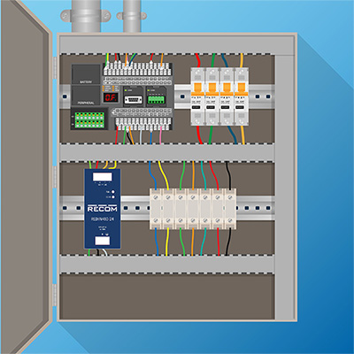 Fig. 1: Typical DIN rail installation
Advantages of the DIN Rail System
Fig. 1: Typical DIN rail installation
Advantages of the DIN Rail System
Firstly, the modular approach allows electrical cabinets and panels to be quickly assembled, moved, or rearranged for optimum use of the available space with only a standard electrician’s screwdriver as a tool. There is no drilling, cutting, or threading needed. Electrical cabinets and panels are often available with pre-installed rails so installation can begin immediately.
Secondly, the DIN rail system allows easy upgrading or repair without disrupting other components – a defective part can be simply unclipped and replaced without affecting the other components. If the new part happens to be slightly larger than the older module, then the existing components can be shifted along the rail to make space.
Thirdly, as the mounting rail dimensions are all standardized, parts from different manufacturers are interchangeable and mounting compatible. On a single rail, different electrical components can be freely mixed, so, for example, connector blocks can be placed next to power supplies to simplify the distribution of power and reduce the amount of cabling required, or actuator relays placed next to PLCs.
Fourthly, as you might expect from a German standard, the ease of mounting allows an organized, neat, and logical layout within the cabinet. This not only speeds up assembly by streamlining the whole construction process but simplifies maintenance and troubleshooting. All electrical contacts are accessible from the front without disconnecting any wiring and many electrical components have status or alarm indicators so that complex installations can be quickly inspected to find the fault.
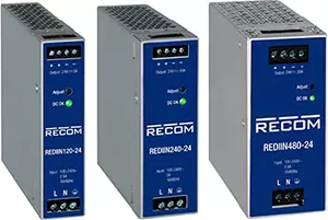 Fig. 2: REDIIN120, REDIIN240, and REDIIN480 DIN rail Power Supplies
Solutions include adding spacers between equipment to allow free air convection to cool the components, repositioning heat-generating components so that they are not in close proximity to one another, or, in extreme cases, adding fans to force-air cool the parts. The vertical separation between rails also needs to be considered so that warm air rising from one component does not adversely affect the component placed immediately above it. Fortunately, software packages are readily available that can be used to both plan the layout of the panel or cabinet in advance and to calculate the expected thermal loading. This software is often offered free by the cabinet manufacturers. More advanced software can also automatically check for compliance with electrical safety, construction, and technical standards, such as EN 61439.
RECOM is an established power supply manufacturer that is well-known for board-mounting or chassis-mounting embedded power, but also offers competitively priced AC/DC DIN rail mount power supplies (Figure 2).
Key Features of DIN Rail Power Supplies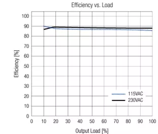 Fig. 3: Flat efficiency curve of the REDIIN120-24. No load power consumption is only 150mW
Design
Fig. 3: Flat efficiency curve of the REDIIN120-24. No load power consumption is only 150mW
Design
The products are fully certified according to international safety standards IEC/EN/UL 62368-1, IEC/EN/UL61010-1, and IEC/EN/UL/CSA61010-2-201. Electromagnetic radiated and conducted emissions are compliant with heavy industrial EN 61000-6-4 Class B Emission standard and EN 61000-6-2 Immunity standard.
The REDIIN series are designed for industrial, automation, power distribution, and test and measurement environments. These slim power supplies are ideal for applications in heavy engineering, production, home automation, data and telecom, traffic control, and water management—anywhere a compact, reliable, and cost-effective DC power supply is required within cabinets or electronic enclosures.
The post Slim DIN Rail Power Supplies For Industrial Applications appeared first on ELE Times.
Turned Commodore Plus4 Keyboard into a MIDI device.
 | Still working on the matrix mapping but it does work besides a few toasted keys. Planning to work on some chord progression/arpeggiator code and connect it to a Korg DS8 of the same era. [link] [comments] |
The Software-Defined Vehicle Revolution: The Engineering Call to Action
The global automotive industry is undergoing its most profound transformation since the assembly line. This shift, driven by electrification and autonomy, is centrally powered by the Software-Defined Vehicle (SDV). For India’s vast pool of electronics and embedded systems engineers, this shift is more than just a trend—it’s a once-in-a-generation opportunity to become a global technology powerhouse in the automotive sector.
The stakes are enormous. India’s software-defined vehicle market is projected to witness a CAGR of 16.56% during the forecast period, FY2026-FY2033, growing from USD 2.69 billion in FY2025 to USD 9.16 billion in FY2033 through hardware, software, and subscription-based features. This piece breaks down the fundamental architectural shift, the commercial imperative driving it, and the precise skills Indian engineers must master to capture this monumental value.
The Architectural Flip: From Distributed Modules to Central Compute
For the last three decades, vehicle architecture was defined by a sprawling, distributed network of Electronic Control Units (ECUs). Modern cars can contain up to 150 dedicated ECUs, each dedicated to a narrow task (such as controlling a specific window or a part of the engine), which are scattered throughout the car.
Christopher Borroni-Bird, Founder of Afreecar, USA, notes, “The path to SDVs is a major disruption for automakers. It is a fundamental shift in value from hardware to software.”
The fundamental limitations of this legacy architecture are now a critical bottleneck for innovation:
- Complexity and Cost: This highly decentralized design requires kilometers of heavy, expensive wiring and complex communication protocols (like CAN and LIN), leading to massive complexity in integration and testing.
- Bandwidth Saturation: The low bandwidth of CAN limits the data throughput required by modern systems like Advanced Driver Assistance Systems (ADAS), which process gigabytes of sensor data per second.
- Inflexible Updates: Functionality is tied tightly to hardware, making it nearly impossible to introduce meaningful new features after the car leaves the factory.
The Software-Defined Vehicle solves this by replacing the distributed ECUs with a centralized, high-performance computing (HPC) approach. It consolidates functions into powerful, centrally or zonally placed compute units. This transformation moves through two key stages:
- Domain-Centralization (The Intermediate Step)
In the domain-centralized architecture, automakers consolidate dozens of small ECUs into a handful of powerful Domain Controllers—typically one each for powertrain, body, infotainment, and ADAS. These domain controllers are high-performance SoCs that replace clusters of ECUs within each functional region. While this significantly reduces ECU count and wiring complexity, it still maintains separation between critical domains. Engineers now need to handle thermal constraints, high-speed data movement, and virtualization middleware to ensure that safety-critical functions (like braking or steering) remain strictly isolated from non-critical ones (like media playback). This stage marks the shift from distributed electronics to consolidated compute, setting the foundation for full vehicle-centralized architectures.
- High-Speed Networking
High-speed networking is essential in SDVs because modern vehicles generate enormous volumes of data from cameras, radar, LiDAR, and other sensors—far beyond what the traditional CAN bus can carry. CAN was designed for millisecond-level control signals, not multi-megabit video streams or real-time sensor fusion. To solve this bottleneck, SDVs now use Automotive Ethernet as the central data backbone. It supports gigabit-level throughput and incorporates Time-Sensitive Networking (TSN) to ensure data is delivered with guaranteed timing, which is critical for ADAS decision-making.
In simple terms: Automotive Ethernet + TSN allows the car’s brain to receive huge amounts of sensor data quickly, predictably, and without delay—something CAN was never built for. This shift enables reliable perception, faster response times, and the scalable communication architecture required for autonomous and software-defined features.
The Commercial Imperative: Recurring Revenue and Lifetime Value
The architectural shift is driven equally by a dramatic change in the business model. Historically, an OEM’s revenue ceased the moment the car was sold. SDVs flip this model, transforming the vehicle into an evolving platform for recurring revenue. The technical architecture in SDVs is merely the enabling layer for an entirely new economic model. When a vehicle’s capabilities are defined by its software stack, the relationship with the customer becomes continuous.
The market potential for subscriptions, services, and features-on-demand is what drives the massive industry investment. Post-sale monetization opportunities include:
- Features-as-a-Service: Performance boosts, advanced ADAS capabilities, or heated seats activated temporarily via a subscription.
- Predictive Maintenance: Using vehicle data to predict failures, leading to service revenue and higher customer satisfaction.
- In-Car Commerce and Telematics: Partnerships for payment processing, insurance optimization, and fleet management services.
The Pillars of SDV Engineering: New Skill Requirements
To build the SDV, engineers must shift their focus from optimizing individual microcontrollers to designing entire systems based on high-performance computing, security, and real-time networking. The core skill pillars for the next generation of Indian automotive engineers are:
- High-Speed, Deterministic Networking
The shift from CAN/LIN (up to 1 Mbit/s) to Automotive Ethernet (100 Mbit/s to 10 Gbit/s) is essential to handle the massive data from LIDAR, radar, and HD cameras. Crucially, engineers must master Time-Sensitive Networking (TSN). TSN is the standard that guarantees deterministic data delivery—meaning a brake command always arrives in a precise, guaranteed timeframe, regardless of network traffic. This is a non-negotiable requirement for functional safety.
- Platform Virtualization and Mixed-Criticality Systems
The HPC runs software with varying safety requirements, known as mixed-criticality systems. A malfunction in the display stack must not crash the brake-by-wire system. This separation is achieved using two key technologies:
- Hypervisors (Type 1): Specialized hypervisors allow multiple operating systems (or execution environments) to run concurrently on the same HPC hardware, ensuring fault isolation and resource partitioning.
- Adaptive AUTOSAR: This next-generation middleware (replacing Classic AUTOSAR) is built to manage the complexity of centralized compute, supporting POSIX-compliant operating systems and service-oriented communication protocols necessary for dynamic, interconnected applications.
3. Functional Safety and Cybersecurity
With software controlling all critical systems, safety standards must be integrated at every layer of the architecture.
- ISO 26262 (Functional Safety): Engineers need proficiency in defining and implementing specific Automotive Safety Integrity Levels (ASIL) for every function. For example, ADAS features might require ASIL-D (the highest level).
- ISO/SAE 21434 (Cybersecurity): Connectivity exposes the vehicle to external threats. Expertise in Threat Analysis and Risk Assessment (TARA), secure boot, intrusion detection systems (IDS), and over-the-air (OTA) update security is mandatory to protect the vehicle throughout its 15-year lifecycle.
India’s Strategic Advantage and the Talent Gap
India is uniquely positioned to capitalize on this shift. The country already hosts the largest R&D and engineering centers outside of headquarters for nearly every global OEM and Tier-1 supplier (e.g., Bosch, Continental, Mercedes-Benz, Hyundai). Indian teams are already responsible for complex areas like Infotainment development, diagnostics, and component-level software.
However, a critical gap exists between foundational embedded skills and the advanced, systems-level expertise required for SDVs. The shortage is most acute in:
- System Architects: We need engineers who can define the holistic E/E architecture, not just code a single ECU. This requires an end-to-end view of hardware, software, networking, and safety protocols.
- High-Level Software (Full-Stack Automotive): Expertise in integrating cloud services (AWS, Azure) with the in-vehicle VOS, leveraging DevOps pipelines, and managing vast data streams for machine learning models running on the car’s edge processors.
- Low-Level Middleware and Safety: Deep competence in Adaptive AUTOSAR and hypervisor configuration, which allows the critical and non-critical software stacks to coexist safely.
The Call to Build
The SDV revolution demands that Indian engineers make a proactive pivot. The value chain is restructuring, and the future winners will be those who design the platforms, not just those who implement modules.
This transition requires investment—not just by multinational corporations, but by individual engineers and educational institutions. Universities must rapidly introduce a curriculum focused on high-speed communications (TSN), virtualization, and modern safety standards. Industry professionals must aggressively pursue certifications and hands-on experience in Adaptive AUTOSAR and HPC environments.
India has the talent base and the sheer numbers to become the world’s SDV hub. This opportunity is about moving up the value chain, leading innovation, and defining the future of mobility from Bengaluru, Pune, and Hyderabad. The vehicle is being redefined, and with the right strategy and swift action, Indian engineers can and must be the global architects of the Software-Defined Vehicle era.
The post The Software-Defined Vehicle Revolution: The Engineering Call to Action appeared first on ELE Times.
Vishay launches 1200V SiC MOSFET power modules in MAACPAK PressFit package
US ITC preliminary determination finds violation of Infineon patent by Innoscience
Ascent provides space company with PV modules for power generation testing in cislunar space
Simulación de una ALU de 16 bits en Proteus
 | Diseñé y simulé una ALU de 16 bits en Proteus, capaz de ejecutar operaciones AND, OR, XOR, SUMA y RESTA (con acarreo). Todo está organizado en módulos para facilitar el análisis, e incluye flags e indicadores para validar el comportamiento de cada operación. Si desean obtener el archivo de simulación, pueden escribirme directamente. [link] [comments] |
LED Fade in
 | Turning led on slowly [link] [comments] |
🍎 День відкритих дверей KPIAbitFest

КПІ ім. Ігоря Сікорського запрошує учнів старших класів ваших закладів освіти долучитися до Дня відкритих дверей — KPIAbitFest, який відбудеться 13 грудня з 10:00 до 13:00 у Бібліотеці КПІ ім. Ігоря Сікорського (проспект Берестейський, 37).
Випускник КПІ увійшов до рейтингу Clarivate найбільш цитованих учених

Юрій Гогоці, професор Університету Дрекселя (США) і випускник Київського політехнічного інституту імені Ігоря Сікорського, увійшов до списку Clarivate найцитованіших дослідників світу у 2025 році.
Nuvoton launches compact 1.7W 402nm violet laser in TO-56 CAN package
A digital filter system (DFS), Part 1

Editor’s note: In this Design Idea (DI), contributor Bonicatto designs a digital filter system (DFS. This is a benchtop filtering system that can apply various filter types to an incoming signal. Filtering range is up to 120 kHz.
In Part 1 of this DI, the DFS’s function and hardware implementation are discussed.
In Part 2 of this DI, the DFS’s firmware and performance are discussed.
Selectable/adjustable bench filterOver the years, I have been able to obtain a lot of equipment needed for designing, testing, and diagnosing electronic equipment. I have accumulated power supplies, scopes, digital voltmeters (DVMs), spectrum analyzers, signal generators, vector network analyzers (VNAs), LCR meters, etc., etc.
One piece of equipment I never found is a reasonably priced lab bench filter—something that would take in a signal and filter it with a filter whose parameters could be set on the front panel.
There are some tools that run on a PC’s sound card, but I don’t like to connect my electronic tests on my PC for fear that I’ll damage the PC. The other issue is that I am looking for something that can go up to 100 kHz or so, which is not typical of many soundcards. So, it was time to try to design one.
Wow the engineering world with your unique design: Design Ideas Submission Guide
What I came up with in a small bench-top device with one BNC input for the signal you want filtered and one BNC output for the resulting filtered signal (Figure 1). It has a touchscreen LCD to select a filter type and the cutoff/center frequency. So, what can it do?
 Figure 1 The finished digital filter system that allows you to select a low-pass, high-pass, band-pass, or band-stop filter type.
You can select a low-pass, high-pass, band-pass, or band-stop filter type. The filter can also be either a two-pole Butterworth or a four-pole.
For the frequency, you can select anywhere from a few Hz to 120 kHz. The are also three gain controls (an analog input gain knob, an analog output gain, and an internal digital gain.)
The cost to build the filter is around $75, as well as some odds and ends you probably already have around.
I also included a download for a 3D printable enclosure. Let’s take a deeper look at this design.
The circuitThe design is centered around a digital filter executed in a Cortex M4 microcontroller (MCU). The three main blocks of the system are an analog front end (AFE), which is composed of four op-amps providing input gain adjustment and antialiasing filtering.
Next is a single board computer (SBC) powered by a Cortex M4. This provides an input for the ADC, controls the LCD and touchscreen, executes the digital filters, and controls the output DAC.
The last block is the analog back end (ABE), which again consists of four op-amps that make up the analog gain circuit and the analog output reconstruction filter.
Let’s take a look at the schematic to see more detail (Figure 2).

Figure 2 The DFS schematic showing the AFE, the ABE, and SBC that provides an input for the ADC, controls the TFT display, executes the digital filters, and controls the output DAC.
Here you can see the blocks we just talked about and a few other minor pieces. Let’s dive a little deeper.
The AFEThe AFE starts by AC-coupling the external signal you want to filter. Then, the first op-amp, after the protection diodes, provides an adjustable gain for the input. This uses a simple single-supply inverting op-amp circuit. RV1 is a potentiometer on the front panel (see Figure 1 above) that allows for a gain of the input from 1x to 5x.
Again, looking at the schematics, we next see a single-pole low-pass filter, which is tuned to 120 kHz. Next are a pair of 2-pole Sallen-Key low-pass filters with components selected to create a Butterworth filter set to 120 kHz.
So now our input signal has been filtered at a frequency that will allow the MCU’s ADC to sample without aliasing. I designed this filter and the ABE filter using TI’s WEBENCH Circuit Designer.
So, we have a 5-pole low-pass filter frontend that will give us a roll-off of 30 dB per octave, or 100 dB per decade.
The flywheel RC circuit is next. As explained in a previous article, the capacitor in this RC circuit provides a charge to hold up the voltage level when the ADC samples the input. More on this can be found at: ADC Driver Ref Design Optimizing THD, Noise, and SNR for High Dynamic Range
The ABEWe’ll skip the MCU for now and jump to the right side of the schematic. Here we see a circuit very similar to the AFE, but this is used as a reconstruction filter that removes artifacts created by the discrete steps used in the MCU’s DAC.
So, starting from the DAC output from the SBC, we see an adjustable gain stage which allows the user, via the output potentiometer, to increase the output level, if desired. This output gain can be adjusted from 1x to 5x.
Next in the schematic, you’ll see two stages of two-pole Sallen-Key low-pass filters configured exactly like the pair in the AFE. So again, they are configured as a 120 kHz Butterworth filter.
The last op-amp circuit in the ABE is a 2x gain stage and buffer. Why a 2x gain stage? I’ll explain more later, but the gist is that the DAC has a limited slew rate compared to the sample rate I used. So, I reduced the value in the DAC by 2 and then compensated for it in this gain stage.
A note about the op-amps used in this design: The design calls for something that can handle 120 kHz passing through a gain of up to 5 and also dealing with the Sallen-Key filters (the TI WEBENCH shows a gain-bandwidth requirement of at least 6 MHz). I also needed a slew rate that could deal with a 120 kHz signal with a level of 3.3 Vpp. The STMicroelectronics TSV782 fit the bill nicely.
The last two components are the resistor and the capacitor before the output BNC connector. The resistor is used to stabilize the op-amp circuit if the output is connected to a large capacitance load. The 1uF capacitor provides AC coupling to the output BNC.
The MCUThe brains used in this design is a Feather M4 Express SBC, which contains a Microchip Technology’s ATSAMD51 that has a Cortex M4 core. This is primarily powered by a USB connection (or a battery we will discuss in Part 2).
This ATSAMD51 has a few ADCs and DACs, and we use one of each in this design. It also has plenty of memory (512 kB of program memory and 192 kB of SRAM).
It runs at a usable 120 MHz and is enhanced with a floating-point processor. All this works nicely for the digital filtering we will explain in Part 2. Other features I used include a number of digital I/O ports, an SPI port, and a few other ADC inputs.
One feature I found very nice on the SBC was a 3.3 VDC linear regulator that not only powers the MCU, but has sufficient output to power all other devices in the design.
On the schematic (Figure 1), you can see that the AFE connects to an ADC input on the SBC, and an SBC DAC connects to the ABE circuit. Another major component is the TFT LCD and touchscreen, powered by the 3.3 VDC coming from the SBC.
Miscellaneous schematic itemsThat leaves a few extra items on the schematic.
Voltage referenceThere are 2 simple ½ voltage dividers to generate 1.65 VDC from the 3.3 VDC supply. One is used on the AFE to get a mid-voltage reference for the single supply op-amp design. This reference is simply two equal resistors and a capacitor connected to ground, and from the center of the series-connected resistors.
A second reference was created for the ABE circuit. I used two references as I was laying this out on a protoboard, and the circuits were separated by a significant distance (without a ground plane).
LED indicatorThere is also an LED used to indicate that the ADC is clipping the signal because the input is too large or too small. Another LED indicates the DAC is clipping for the same reasons. There will be more discussion on this in the firmware section in Part 2.
Floating groundAn interesting feature of the SBC is that it contains the charging circuit for a lithium polymer 3.7-V battery. This is optional in the design, but it does allow you to operate the DFS with a floating ground and a quiet voltage supply, which may help in your testing.
EnableA somewhat unique feature, which turns out to be helpful, is an enable that is used to turn off the system if you pull it to ground.
If you use a battery, along with the USB, and want to use a typical power on/off switch, you would need to break the incoming USB line and the battery line, which makes it a 2-pole switch.
So, to get the DFS to power down, I pull the enable line to ground using a 3-pole SPDT switch, which I found has the typical “O/I” on/off indications. You can use a SPST switch; this will have to be switched to “I” to shut it down and “O” to turn it on.
USB voltage displayA ½ voltage divider, with a filter capacitor, is connected to the USB input and used as an input to one of the ADCs, so we can display the connected USB voltage.
Optional resetThe last item is an optional reset. I did not provide a hole to mount a pushbutton, but you can drill a hole in the back of the enclosure for a normally-open pushbutton.
More informationThis device is a fairly easy to build. I built the circuit on a protoboard with SMT parts (thru-hole would have been easier). Maybe someone would like to lay out a PCB and share the design. I think you’ll find this DFS has a number of uses in your lab/shop.
The schematic, code, 3D print files, links to various parts, and more information and notes on the design and construction can be downloaded at: https://makerworld.com/en/@user_1242957023/upload
Editor’s Note: Stay tuned for Part 2 to learn more about the device’s firmware.
Damian Bonicatto is a consulting engineer with decades of experience in embedded hardware, firmware, and system design. He holds over 30 patents.
Phoenix Bonicatto is a freelance writer.
Related Content
- Non-linear digital filters: Use cases and sample code
- A beginner’s guide to power of IQ data and beauty of negative frequencies – Part 1
- A Sallen-Key low-pass filter design toolkit
- Designing second order Sallen-Key low pass filters with minimal sensitivity to component tolerances
- Toward better behaved Sallen-Key low pass filters
- Design second- and third-order Sallen-Key filters with one op amp
The post A digital filter system (DFS), Part 1 appeared first on EDN.
Silly simple precision 0/20mA to 4/20mA converter

This Design Idea (DI) offers an alternative solution for an application borrowed from frequent DI contributor R. Jayapal, presented in: “A 0-20mA source current to 4-20mA loop current converter.”
It converts a 0/20mA current mode input, such as produced by some process control instrumentation, into a standard industrial 4/20mA current loop output.
Wow the engineering world with your unique design: Design Ideas Submission Guide
Figure 1 shows the circuit. It’s based on a (very) old friend—the LM337 three-legged regulator. Here’s how it works.

Figure 1 U1 plus R1 through R5 current steering networks convert 0/20mA input to 4/20mA output.
The fixed resistance of the R1 + R2 + R3 series network, working in parallel with the adjustable R4 + R5 pair, presents a combined load of 312 ohms to the 1.25v output of U1. That causes a zero-input current draw of 1.25/312 = 4 mA, trimmed by R5 (see calibration sequence detailed later).
Summed with this is a 0 to 16 mA current derived from the 0 to 20 mA input, controlled by the 4:1 ratio current split provided by the R1/R2/R3 current divider and fine trimmed by R2 (ditto).
Note that 4 mA is below the guaranteed minimum regulation current specification for the LM337. In fact, most will work happily with half that much, but you might get a greedy one. So just be aware.
The result is a precision conversion of the 0 to 20mA input to an accurate 4 to 20mA loop current. Conversion precision and stability are insensitive to R2 trimmer wiper resistance due to the somewhat unusual input topology in play.
Calibration proceeds in a four-step linear (iteration-free one-pass) sequence consisting of:
- Set input = 0.0 mA.
- Adjust R5 for 4.00 mA loop current.
- Set input = 20.00 mA.
- Adjust R2 for 20.00 mA loop current.
Done.
The input voltage burden is a negative 1.0 volt. The output loop voltage drop is 4 volts minimum to 40 volts maximum. The maximum ambient temperature (with no U1 heatsink) is 100oC. Resistors should be precision types, and the trimmer pots should be multiturn cermet or similar.
Stephen Woodward’s relationship with EDN’s DI column goes back quite a long way. Over 100 submissions have been accepted since his first contribution back in 1974.
Related Content
- A 0-20mA source current to 4-20mA loop current converter
- A two-wire temperature transmitter using an RTD sensor
- Two-wire interface has galvanic isolation
- Low-cost NiCd battery charger with charge level indicator
- Single phase mains cycle skipping controller sans harmonics
- Two-wire remote sensor preamp
The post Silly simple precision 0/20mA to 4/20mA converter appeared first on EDN.
Подорож працівників КПІ до Закарпаття

Нещодавно члени університетської профспілкової організації здійснили захопливу подорож до одного з наймальовничіших куточків України – у неповторне Закарпаття. Цей край завжди приваблював туристів своєю природною красою, багатою історією, архітектурою та особливим колоритом. Програма подорожі була насиченою, пізнавальною і, водночас, дарувала можливості відпочинку та приємного спілкування в колі колег. Київські політехніки спочатку потягом доїхали до Ужгорода, а звідти вже мандрували автобусом.
Команда студентів КПІ – серед переможців хакатону "Безпечне майбутнє"

В столиці України відбувся Всеукраїнський хакатон "Безпечне майбутнє: концепція VR/AR-тренажера для підготовки саперів", організований Міністерством економіки, довкілля та сільського господарства України спільно з національною платформою Demine Ukraine, Центром гуманітарного розмінування
Big opportunity for India to fill the 700,000 worker shortage in the chip industry : IESA chief Ashok Chandak
Speaking at the CNBC-TV18 and Moneycontrol UP Tech Next Electronics and Semiconductor Summit on December 2 in Lucknow, president of the India Electronics and Semiconductor Association (IESA), Ashok Chandak stated that the global chip industry faces a deficit of 700,000 workers by 2030, and this can be used as a potential opportunity by India to fill the urgent gap.
Highlighting this opportunity, Chandak also threw light on the existing lack of skill training curriculum. For this he suggested a two-step model, updating technical curriculum to meet future needs and building manufacturing-related training programmes as India scales chip production.
He also added that IESA has already begun discussions with institutes on curriculum reform.
As the advancement in the industry continues to grow, the skill set required also needs to be updates and modified accordingly. The assimilation of Ai and machine learning with the use of technologies like digital twin and AR/VR have opened up the potential for the large Indian population of engineers and scientists to fulfil the demand as India strides ahead on its own India Semiconductor Mission (ISM), wherein the first ‘Made In India’ chip is expected to roll out by the end of December 2025.
The post Big opportunity for India to fill the 700,000 worker shortage in the chip industry : IESA chief Ashok Chandak appeared first on ELE Times.
👍 Долучайтесь до встановлення рекорду України

Минулого року КПІшниками вже втретє був встановлений національний рекорд щодо найбільшої кількості антен, виготовлених за 24 години.
Не зупиняємося і запрошуємо долучатися до чергового оновлення рекорду України!
I spent several hours learning a 7-segment display to show this to my coworker.
 | Used a 5V regulator, 2 buttons and 2 NPN transistors to control the shared segment. I am still learning, this was my first attempt at trying a project without copying a YouTube tutorial. [link] [comments] |
Cree LED and SANlight partner on high-efficiency horticulture lighting
Outages Won’t Wait: Why Grid Modernization Must Move Faster
Courtesy: Keysight Technologies
A routine click on a recommended link via the AI overview of my browser on November 18 yielded a glaring “internal server error” (Figure 1) when I clicked on a search-referenced website. The Cloudflare outage disrupted connectivity on various platforms, including ChatGPT, Canva, and X. Undaunted, the cyber community had a memes field day when services were restored, flooding their feeds with humorous outage memes.
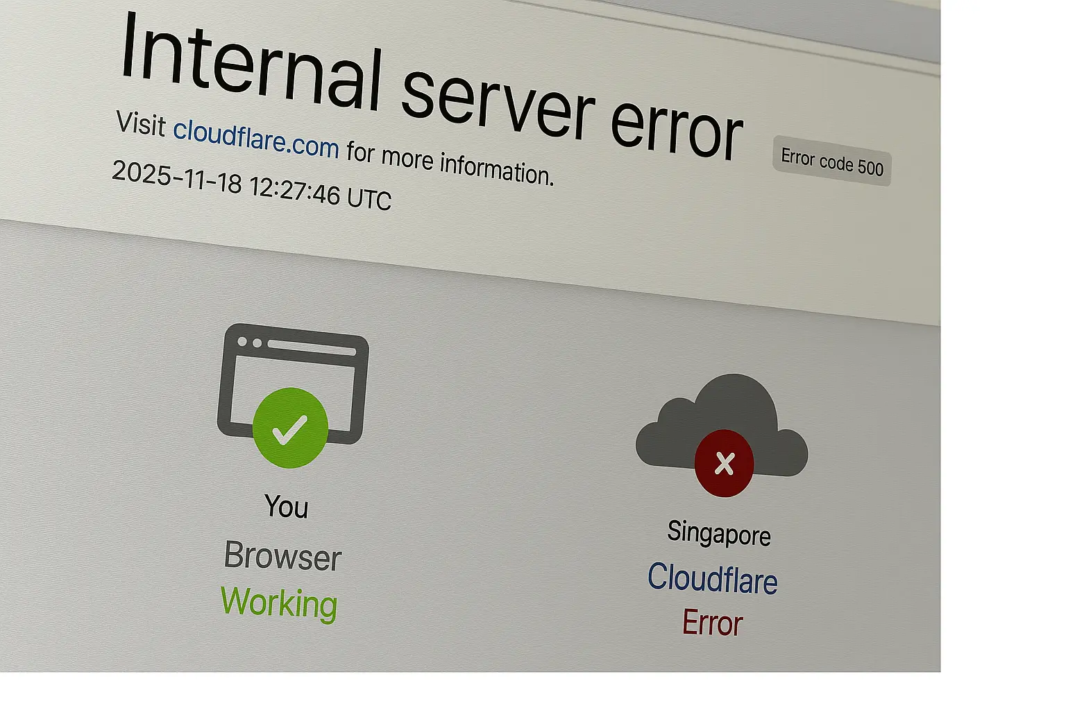 Fig1. Data center downtime can cause a host of end-user disruptions.
On a more serious note, data center and internet outages are no laughing matter, impacting businesses from online shopping to cryptocurrency exchanges. While the November outage at Cloudflare was attributed to configuration errors, another outage two years earlier was due to a power failure at one of its data centers in Oregon. Cloudflare is not alone in its outage woes. In fact, power failures outweigh network and IT issues when it comes to disrupting online user experiences.
Data from the 2025 Uptime Institute Global Data Center Survey shows that although 50% of data centers experienced at least one impactful outage over the past three years, down from 53% in 2024 (see Figure 2), power issues remain the top cause.
 Figure 2. Grid modernization is key to addressing power issues causing data center outages.
It’s not surprising that just a few years ago, electric vehicles (EVs) were deemed to be the new energy guzzlers of the decade, only to be rapidly overtaken by data centers. From crypto mining to generating “morph my cat to holiday mode” image creation prompts, each click adds strain to the power grid, not forgetting the heat generated.
 Figure 3. Meta AI’s response when asked how much energy it used to turn my homebody kitty into a cool cat on vacation.
Why must grid modernization happen sooner rather than later?
Data centers currently consume almost five times as much electricity as electric vehicles collectively, but both markets are expected to see a rise in demand for power in the coming years. In developed countries, power grids are already feeling the strain from these new energy guzzlers. Grid modernization must happen sooner rather than later to buffer the impact of skyrocketing electricity demand from both data centers and the EV market, to ensure the power grid’s resilience, stability, and security. Without swift upgrades, older grids are at risk of instability, outages, and bottlenecks as digital infrastructure and EV adoption accelerate.
What does grid modernization entail?
Grid modernization requires a strategic overhaul of legacy power infrastructure at the energy, communications, and operations levels, as illustrated in Figure 4. Existing energy infrastructure must be scalable and be able to incorporate and integrate renewable and distributed energy resources (DERs). Bi-directional communication protocols must continue to evolve to enable real-time data exchange between power-generating assets, energy storage systems, and end-user loads.
This transformation demands compliance with rigorous interoperability standards and cybersecurity frameworks to ensure seamless integration across heterogeneous systems, while safeguarding grid reliability and resilience against operational and environmental stresses.
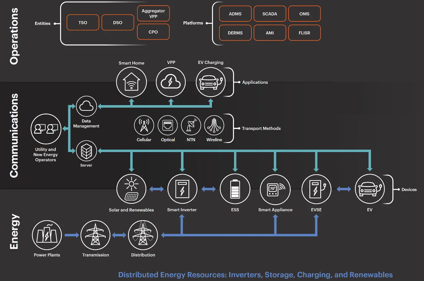 Figure 4. Grid modernization impacts a complex, interconnected energy ecosystem that must be thoroughly tested and validated to ensure grid reliability and resilience.
Towards Grid Resilience
Grid modernization can significantly reduce both data center outages and power shortages for EV charging, although the impact will depend on how fast the power infrastructure gets upgraded. The modernized grid will employ advanced sensors, automated controls, and predictive analytics to detect and isolate faults quickly. This will further reduce the number of data center outages due to power issues and mitigate the dips in power currently plaguing some cities’ EV charging infrastructure. As the world powers on with increasing load demands, our grid energy community must work together to plan, validate, and build a resilient grid.
Keysight can help you with your innovations for this exciting grid transformation. Our design validation and testing solutions cover inverter-based resources (IBRs) and distributed energy resources (DERs), to tools enabling systems integration and deployment, as well as operations.
The post Outages Won’t Wait: Why Grid Modernization Must Move Faster appeared first on ELE Times.
Pages


![[link]](https://i.redd.it/42byuxq9v05g1.jpeg)