
Feed aggregator
Спільний проєкт з Київським метрополітеном «Метро. Місто. Політехніка»

Запрошуємо переглянути цікаві інформаційні плакати у спільному проєкті з Київським метрополітеном «Метро. Місто. Політехніка» щодо важливих інженерних рішень у київському метрополітені, які були впроваджені за участі фахівців з КПІ (зокрема, щодо будівництва станції «Політехнічний інститут»).
Trump Plans to Impose 100% Tariff on Computer Chips, Likely Driving Up Electronics Prices
President Donald Trump announced plans to impose a 100% tariff on computer chips, which would certainly increase the price of gadgets, cars, home appliances, and other items considered necessary for the digital age.
Speaking from the Oval Office alongside Apple CEO Tim Cook, Trump said, “There will be a tariff of approximately 100% on chips and semiconductors. In order to increase the company’s domestic investment commitment and possibly avoid future iPhone levies, Trump also declared that Apple would invest an additional $100 billion in the US.
However, companies that manufacture semiconductors within the United States would be exempt from these tariffs.
Effect Across Industries
Chips for computers are the crucial element in question. For consumer gadgets, cars, home appliances, and industrial systems, that is the solution to the usage of current technology.
Shortages of chips in the middle of the COVID-19 pandemic caused inflation in prices and disruptions in the supply chain. Global chip sales have grown by 19.6% over the past year, indicating strong demand.
Trump’s approach deviates from the CHIPS and Science Act’s deliberate approach. The law was signed in 2022 by President Joe Biden with a promise of $50 billion worth of subsidies, tax breaks, and research funding for domestic chip production.
Conclusion:
While it is meant to strengthen U.S. manufacturing, many critics warn that this policy might backfire. Hence, as chips cost more, profits get thinner while companies hike consumer prices. No official word has so far come from these titans of electronics, Nvidia and Intel, concerning the announcement.
The post Trump Plans to Impose 100% Tariff on Computer Chips, Likely Driving Up Electronics Prices appeared first on ELE Times.
eDesignSuite Power Management Design Center: 3 new features and a ton of possibilities
By: STMicroelectronics
eDesignSuite Power Management Design Center is more than just a new console, but a new way to choose more responsible products, simulate higher loads, and shave weeks off the design phase of power circuits. The suite includes a power supply and LED lighting design tool, a digital workbench, and a power tree designer. Concretely, ST is now supporting 30 kW applications, and users can expect support for even greater power solutions as we update our web application. Put simply, engineers have access to new customization and simulation capabilities, which expand the scope of the Power Management Design Center and lower the barrier to entry for power application design.
eDesignSuite Power Management Design Center: New console Screenshot of eDesignSuite Power Management Design Center
Users will instantly be familiar with the new console of the Power Management Design Center because it remains extremely close to the version ST launched when we moved to HTML 5. After all, its intuitiveness is a key component for engineers working on complex power applications. What has primarily changed is that we are now offering the ability to highlight devices considered “responsible”, meaning they enhance energy efficiency. Behind the scenes, it required us to create new categories and labels, update our databases, and determine which devices would have the most significant impact on a design. For users, all it takes is a single click to know how to optimize their design meaningfully.
And this is just the beginning. We are already working on providing impact simulations to ensure designers can concretely see how choosing a responsible device affects their design. Too often, engineers recognize that a gain of just one percentage point in efficiency can make a significant difference. Unfortunately, communicating this fact can be as tricky. That’s why we are working to make eDesignSuite a scientific witness of what it means to design with responsible solutions, such as helping determine the amount of greenhouse emissions saved and other real-world environmental benefits. In a nutshell, we are taking the simulation engine that has made eDesignSuite so popular and using its rigorous models to make “responsible” a lot more tangible.
New topologiesThe Digital Workbench in eDesignSuite Power Management Design Center got support for new topologies that primarily focus on energy storage. Interestingly, some topologies exhibit bidirectional behavior, playing a crucial role in designing systems that not only supply power to battery chargers, such as those in electric vehicles, but also enable power to be fed back to the grid or homes, as seen in Vehicle-to-Grid (V2G) and Vehicle-to-Home (V2H) applications. These new topologies are especially promising when working with gallium nitride or silicon carbide. Their arrival in Digital Workbench means that engineers can now use our wizard to expedite their development and more accurately size the other components of their design, among other benefits.
ST will continue to innovate by introducing advanced topologies. Recently, we launched a 7 kW two-channel multilevel buck converter and a 10 kW two-channel multilevel boost converter, both featuring Maximum Power Point Tracking (MPPT), which aids in designing for solar applications. Indeed, as solar energy is a volatile source due to frequent fluctuations caused by the sun’s movement or clouds, it is imperative to track these changes to optimize power conversion. That requires an MCU like the STM32G4 and a topology capable of handling these constraints. By offering such new topologies in Digital Workbench, engineers can significantly reduce their time-to-market.
New electro-thermal simulationThe fact that we are supporting new topologies and offering a new console highlights the unique demands engineers are facing. As markets require more efficient systems, simulations are ever more critical. That’s why eDesignSuite also got a new electro-thermal simulator, the so-called PCB Thermal Simulator. In a nutshell, it opens the door to temperature analysis based on the electrical performance of a PCB by simply analyzing Gerber files.
Specifically, by using a precise thermal model and iterative calculations, the ST PCB Thermal Simulator quickly and precisely estimates temperatures on both sides of the board. It can also simulate inner layers and allows manual or automatic placement of heat sources (custom or predefined devices), heat sinks, copper areas, and thermal vias. Simulation results are displayed as colored maps overlaid on both sides of the board. Users can inspect any point for temperature values and export results as CSV files. Hence, while the first applications of the electro-thermal simulator primarily focused on motor control, others are now starting to adopt the technology, and we are ensuring that more industries can benefit from it.
The post eDesignSuite Power Management Design Center: 3 new features and a ton of possibilities appeared first on ELE Times.
India’s Electronics Industry Booms with 127% Export Growth in Mobiles
Over the last decade, the electronics manufacturing sector in India has undergone a massive transformation to become a great production center. The sector has witnessed immense growth, both in terms of output and exports, due to some strategic government measures and the rise in foreign investment.
Creating quite a buzz in 2014 was a relatively modest electronic labor market in India, while now, by 2025, it has transformed into a full-blown ecosystem. The value of electronic products made has multiplied six times, and exports have increased eightfold, all pointing toward the enhanced global competitiveness of the sector.
Mobile Manufacturing takes center stage, the mobile segment has witnessed the explosive growth. While in 2014, there were only two manufacturing units, now India has 300 manufacturing facilities. Production has ascended from ₹18,000 crore to ₹5.45 lakh crore, and exports have increased from ₹1,500 crore to ₹2 lakh crore, that is 127% growth.
Policy Reforms:
The government-led PLI scheme is one of the aspects that contributed to this change. The scheme takes in investment upward of ₹13,000 crore and causes production of nearly ₹8.57 lakh crore, as well as creation of more than 1.35 lakh direct jobs. The scheme’s impact on international trade is demonstrated by the ₹4.65 lakh crore in export data.
Inflows of FDI and Semiconductor Push
The Semicon India programme being carried out under six projects is undergoing investments of more than Rs 1.55 trillion and is expected to create over 27,000 direct jobs and build a solid chip-making ecosystem.
Foreign direct investment into electronics manufacturing has now crossed $4 billion since FY21, and around 70% of this inflow is linked to PLI beneficiaries. This is the investing community`s vote of confidence.
With a budget of ₹22,919 crore, the Electronics Components Manufacturing Scheme (ECMS) was introduced with the goal of increasing domestic capabilities and decreasing reliance on imports.
It is purported that one direct job in electronics sector results in three indirect jobs, thus substantially contributing to the broader socio-economic impacts in the country.
Conclusion:
India’s electronics rush is not just numerically driven, but strategically poised for attaining self-reliance and global influence and technological leadership. With this momentum intact, the country is moving to become a major force in the global electronics supply chain.
The post India’s Electronics Industry Booms with 127% Export Growth in Mobiles appeared first on ELE Times.
Machine Learning Architecture Definition, Types and Diagram
Machine learning architecture means the designing and organizing of all of the components and processes that constitute an entire machine learning system. The ML Architecture lays down the framework to design machine learning systems, indicating how data is to be handled, models to be built and analyzed, and predictions to be made. Depending on the particular use case and the set of requirements, the architecture can vary.
A highly scalable and performant machine learning system can be realized through proper architecture.
Types of Machine Learning Architecture:
- Supervised Learning Architecture Unsupervised Learning Architecture
By definition, Supervised Learning uses labeled data to train models: this means each input has a corresponding correct output value. The supervised learning architecture begins with gathering the datasets-full labeled, then undergoes Data Preprocessing to make sure the labels match up with the inputs correctly. Afterward, with the data ready, it proceeds to training it with the algorithm, like Linear Regression, Logistic Regression, SVM, or Random Forests. This method is very suitable when making predictions like: House Price Predictions, Email classifications as Spam or Not Spam, Medical diagnoses based on test results. Supervised learning’s primary benefit is its excellent accuracy when given clean, properly labelled data. It necessitates a lot of labelled data, though, and its preparation can be costly and time consuming.
- Unsupervised Learning Architecture
In unsupervised learning, unlabeled data is used. Hence, the system tries to find the patterns or the clusters without much explicit guidance. Data acquisition for this architecture is more flexible because no labels are required. Preprocessing, however, serves a vital purpose in ensuring the data is consistent and meaningful. Algorithms used in unsupervised learning include K-Means Clustering, Hierarchical Clustering, and PCA. This approach is applicable in customer segmentation, anomaly detection, or market basket analysis. The biggest attraction for unsupervised systems is that they work on data that is generally easier to come by. But since results fundamentally depend on pattern discovery, interpretation of such results may require domain knowledge.
- Reinforcement learning
Reinforcement learning is based on the principle of learning through the interaction with an environment. The architecture is designed to have a setting representing the environment, where a model will choose an action and get feedback on that action being rewarded or penalized. This feedback interchanges are insect within the structure that meanwhile allows model improvement from trial and error. Some popular algorithms are Q-Learning, Deep Q-Networks (DQN), and Policy Gradient methods.
Reinforcement learning finds its way into robots, game AI, and autonomous systems. Its strongest suit is adapting to a dynamic environment wherein the reward is a function of a series of other actions. Hence training can take ages and require a lot of computing power.
Machine Learning Architecture Diagram:
An overview of the many different parts required to create a machine learning application is given by a machine learning architecture diagram.
Simple Machine Learning Architecture Diagram:
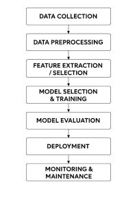
Explanation of the Machine Learning Architecture Diagram:
The diagram outlines the step-by-step process of building and running a machine learning system.
- Data Collection – It helps to treat data as raw material that comes to the project from some arbitrary source like a data base, sensor, API, or web scraping.
- Data Preprocessing – Raw data are often incomplete or inconsistent. In this stage, the data are cleaned and formatted and then prepared so that the model understands them. This is a stage of utmost importance for accuracy.
- Feature Extraction / Selection – Some data is never as useful as others. Herein, the most important variables (features) that determine predictions are picked and retained while other ones that are irrelevant are discarded.
- Model Selection & Training – The type of problem being solved will determine the algorithm choice; the model is then fitted with the historical data to learn patterns and relationships.
- Model Evaluation – The model is tested on new data to assess its accuracy, efficiency, and ability to make real predictions.
- Deployment – Once the model works fine, it is incorporated into a live application or system for real-time prediction or decision-making.
- Monitoring & Maintenance – The model goes through performance tracking as time passes by. It shall be updated or re-trained every time its accuracy is compromised due to real-world data change.
The feedback loop often sends the process to the earlier stages due to new data, ensuring the improvement of the model all the time.
Conclusion:
Machine Learning architecture is more than just a technical plan it is a backbone that decides how well an ML system learns, adapts to changes, and gives out results. A bad architecture disrupts data flow, creates delays in training, and compromises the reliability of predictions over time. Properly-designed ML architectures can be used by businesses and researchers to address problems accurately and at scale. As data grows and technologies evolve, these architectures shall continue to be the power that fuels innovations that re-shape industries by helping people make better decisions while changing everyday life.
The post Machine Learning Architecture Definition, Types and Diagram appeared first on ELE Times.
KYOCERA AVX INTRODUCES NEW HERMAPHRODITIC WTW & WTB CONNECTORS
The new 9288-000 Series connectors enable quick, easy, and tool-free in-field termination; establish durable, reliable, high-integrity connections; and deliver excellent electrical and mechanical performance in lighting and industrial applications.
KYOCERA AVX, a leading global manufacturer of advanced electronic components engineered to accelerate technological innovation and build a better future, released the new 9288-000 Series hermaphroditic wire-to-wire (WTW) and wire-to-board (WTB) connectors for lighting and industrial applications.
These unique two-piece connectors facilitate WTW termination with two identical mating halves, which simplifies BOMs, and WTB termination with one those halves and an SMT version. Both halves of the new 9288-000 Series hermaphroditic connectors feature orange or white glass-filled PBT insulators equipped with plastic latches for good mechanical retention and the company’s field-proven poke-home contact technology, which enables quick, easy, and tool-free in-field wire termination. Simply strip and poke wires to insert and twist and pull to extract. Made of phosphor bronze with lead-free tin-over-nickel plating, these poke-home contacts also establish durable, reliable, high-integrity connections and deliver excellent electrical and mechanical performance.
The new 9288-000 Series hermaphroditic WTW and WTB connectors are currently available with 2–4 contacts on a 5mm pitch, compatible with 16–18AWG solid or stranded wire, and rated for 6A (18AWG) or 7A (16AWG), 600VACRMS or the DC equivalent, 20 mating cycles, three wire replacement cycles, and operating temperatures extending from -40°C to +125°C. They are also UL approved and RoHS compliant and shipped in tape and reel or bulk packaging.
“The new 9288-000 Series hermaphroditic wire-to-wire and wire-to-board connectors leverage our field-proven poke-home contact technology to enable quick, easy, and tool-free in-field termination and durable phosphor bronze contact materials to deliver excellent electrical and mechanical performance throughout the product lifecycle,” said Perrin Hardee, Product Marketing Manager, KYOCERA AVX. “They also feature a locking mechanism to further improve reliability, and WTW versions simplify BOMs since they’re comprised of two of the same part number.”
The post KYOCERA AVX INTRODUCES NEW HERMAPHRODITIC WTW & WTB CONNECTORS appeared first on ELE Times.
Animusic
 | Built Ani Music 🎵 – a pocket PCB piano powered by RC oscillators and NPN transistors. [link] [comments] |
Switched-Capacitor Design Boosts Inverter Efficiency to 96.5%
Зустріч студентів з CEO та засновником Axon Enterprise

🇺🇦🇺🇸 У КПІ ім. Ігоря Сікорського відбулася зустріч студентів з CEO та засновником Axon Enterprise – одного зі світових лідерів у сфері технологій громадської безпеки
Accelerator improves RAID array management

Microchip’s Adaptec SmartRAID 4300 series of NVMe RAID storage accelerators speeds access to NVMe storage in AI data centers. It achieves this through a disaggregated architecture that separates storage software from the hardware layer, leveraging dedicated PCIe controllers to offload CPU processing and accelerate RAID operations. Microchip reports the SmartRAID 4300 achieves up to 7× higher I/O performance compared to the previous generation in internal testing.

In the SmartRAID 4300 architecture, storage software runs on the host CPU while the accelerator offloads parity-based redundancy tasks, such as XOR operations. This allows write operations to bypass the accelerator and go directly from the host CPU to NVMe drives at native PCIe speeds. By avoiding in-line bottlenecks, the design supports high-throughput configurations with up to 32 CPU-attached x4 NVMe devices and 64 logical drives or RAID arrays. It is compatible with both PCIe Gen 4 and Gen 5 host systems.
The SmartRAID 4300 accommodates NVMe and cloud-capable SSDs for versatile enterprise deployments. It uses architectural techniques like automatic core idling and autonomous power reduction to optimize efficiency. The accelerator also provides security features, including hardware root of trust, secure boot, attestation, and Self-Encrypting Drive (SED) support to ensure data protection.
For information on production integration, contact Microchip sales or an authorized distributor here.
The post Accelerator improves RAID array management appeared first on EDN.
Rugged film capacitors off high pulse strength

EPCOS B3264xH double-sided metallized polypropylene film capacitors from TDK withstand pulse stress up to 6500 V/µs. Suited for resonant topologies—particularly LLC designs—these compact, AEC-Q200-compliant capacitors operate continuously from -55°C to +125°C, ensuring reliable performance in harsh environments.

The capacitors cover a rated DC voltage range of 630 V to 2000 V with capacitance values from 2.2 nF to 470 nF. Their specialized dielectric system, combining polypropylene with double-sided metallized PET film electrodes, enables both high pulse strength and current handling. These characteristics make them well-suited for onboard chargers and DC/DC converters in xEVs, as well as uninterruptible power supplies, industrial switch-mode power supplies, and electronic ballasts.
TDK reports that B3264xH capacitors offer high insulation resistance, low dissipation factor, and strong self-healing properties, resulting in a 200,000-hour service life at +85°C and full rated voltage. They are available in three lead spacings—10 mm, 15 mm, and 22.5 mm—to allow integration in space-constrained circuit layouts.
The post Rugged film capacitors off high pulse strength appeared first on EDN.
Hybrid redrivers aid high-speed HDMI links

With integrated display data channel (DDC) listeners, Diodes’ 3.3-V, quad-channel hybrid ReDrivers preserve HDMI signal integrity for high-resolution video transmission. The PI3HDX12311 supports HDMI 2.1 fixed rate link (FRL) signaling up to 12 Gbps and transition-minimized differential signaling (TMDS) up to 6 Gbps. The PI3HDX6311 supports HDMI 2.0 at up to 6 Gbps.

Both devices operate in either limited or linear mode. In HDMI 1.4 applications, they function as limited redrivers, using a predefined differential output swing—set via swing control—to maintain HDMI-compliant levels at the receptacle. For HDMI 2.0 and 2.1, they switch to linear mode, where the output swing scales with the input signal, effectively acting as a trace canceller. This mode remains transparent to link training signals and, in the PI3HDX12311, supports 8K video resolution and data rates up to 48 Gbps (12 Gbps per channel).
The PI3HDX12311 and PI3HDX6311 provide Dual-Mode DisplayPort (DP++) V1.1 level shifting and offer flexible coupling options, allowing AC, DC, or mixed coupling on both input and output signals. To reduce power consumption, the devices monitor the hot-plug-detect (HPD) pin and enter a low-power state if HPD remains low for more than 2 ms.
In 3500-unit quantities, the PI3HDX12311 costs $0.99 each, and the PI3HDX6311 costs $0.77 each.
The post Hybrid redrivers aid high-speed HDMI links appeared first on EDN.
Bluetooth 6.0 modules target varied applications

KAGA FEI is expanding its Bluetooth LE portfolio with two Bluetooth 6.0 modules that offer different memory configurations. Like the existing EC4L15BA1, the new EC4L10BA1 and EC4L05BA1 are based on Nordic Semiconductor’s nRF54L series of wireless SoCs and integrate a built-in antenna.

The EC4L15BA1 offers the highest memory capacity, with 1.5 MB of NVM and 256 KB of RAM. For applications with lighter requirements, the EC4L10BA1 includes 1.0 MB of NVM and 192 KB of RAM, while the EC4L05BA1 provides 0.5 MB of NVM and 96 KB of RAM. This range enables use cases from industrial IoT and healthcare to smart home devices and cost-sensitive, high-volume designs.
The post Bluetooth 6.0 modules target varied applications appeared first on EDN.
CCD sensor lowers noise for clearer inspections

Toshiba’s TCD2728DG CCD linear image sensor uses lens reduction to cut random noise, enhancing image quality in semiconductor inspection equipment and A3 multifunction printers. As a lens-reduction type sensor, it optically compresses the image before projection onto the sensor. According to Toshiba, the TCD2728DG has lower output amplifier gain than the earlier TCD2726DG and reduces random noise by about 40%, down to 1.9 mV.

The color CCD image sensor features 7500 image-sensing elements across three lines, with a pixel size of 4.7×4.7 µm. It supports a 100-MHz data rate (50-MHz × 2 channels), enabling high-speed processing of large image volumes. This makes it well-suited for line-scan cameras in inspection systems that require real-time decision-making. A built-in timing generator and CCD driver simplify integration and help streamline system development.
The sensor’s input clocks accept a CMOS-level 3.3-V drive. It operates with 3.1- V to 3.5-V analog, digital, and clock driver supplies (VAVDD, VDVDD, VCKDVDD), plus a 9.5-V to 10.5-V supply for VVDD10. Typical RGB sensitivity values are 6.7 V/lx·s, 8.5 V/lx·s, and 3.1 V/lx·s, respectively.
Toshiba has begun volume shipments of the TCD2728DG CCD image sensor in 32-pin WDIPs.
Toshiba Electronic Devices & Storage
The post CCD sensor lowers noise for clearer inspections appeared first on EDN.
Micron Unveils PCIe Gen6 SSDs to Power the Next Wave of AI Data Centers
Car speed and radar guns

The following would apply to any moving vehicle, but just for the sake of clear thought, we will use the word “car”.
Imagine a car coming toward a radar antenna that is transmitting a microwave pulse which goes out toward that car and then comes back from that car in a time interval called “T1”. Then that same radar antenna transmits a second microwave pulse that also goes out toward that still oncoming car and then comes back from that car, but in a time interval called “T2”. This concept is illustrated in Figure 1.
 Figure 1 Car radar timing where T1 is the time it takes for a first pulse to go out toward a vehicle get reflected back to the radiating source, and T2 is the time it takes for a second pulse to go out toward the same vehicle and get reflected back to the radiating source.
The further away the car is, the longer T1 and T2 will be, but if a car is moving toward the antenna, then there will be a time difference between T1 and T2 for which the distance the car has moved will be proportional to that time difference. In air, that scale factor comes to 1.017 nanoseconds per foot (ns/ft) of distance (see Figure 2).

Figure 2 Calculating roundtrip time for a radar signal required to catch a vehicle traveling at 55 mph and 65 mph.
Since we are interested in the time it takes to traverse the distance from the antenna to the car twice (round trip), we would measure a time difference of 2.034 ns/ft of car travel.
A speed radar measures the positional change of an oncoming or outgoing car. Since 60 mph equals 88 ft/s, we know that 55 mph comes to (80+2/3) ft/s. If the interval between transmitted radar pulses were one pulse per second, a distance of (80+2/3) feet would correspond to an ABS(T1-T2) time difference of 164.0761 ns. A difference in time intervals of more than that many nanoseconds would then be indicative of a driver exceeding a speed limit of 55 mph.
For example, a speed of 65 mph would yield 193.9081 ns, and on most Long Island roadways, it ought to yield a speeding ticket.
John Dunn is an electronics consultant, and a graduate of The Polytechnic Institute of Brooklyn (BSEE) and of New York University (MSEE).
Related Content
- Mattel makes a real radar gun, on the cheap
- Simple Optical Speed Trap
- Whistler’s DE-7188: Radar (And Laser) Detection Works Great
- Accidental engineering: 10 mistakes turned into innovation
The post Car speed and radar guns appeared first on EDN.
Skyworks’s June-quarter revenue, gross margin and EPS exceed guidance
My grandpa's handmade intercom system from the communist era (~1980)
") | submitted by /u/Victor464543 [link] [comments] |
Top 10 Machine Learning Algorithms
The term ‘machine learning’ is used to describe the process of turning the machines smarter day by day in today’s technologically advanced environment. Machine learning serves as the foundation for the creation of voice assistants, tailored recommendations, and other intelligent applications.
The core of this intelligence is the machine learning algorithm, through which a computer learns from data and then makes decisions to some lower or higher extent without human intervention.
This article will explore what these algorithms are, the types, and their common daily life application, in addition to the top 10 machine learning algorithms.
Machine learning algorithms are sequences of instructions or models that allow computers to learn patterns from data and make decisions or prediction under conditions of uncertainty without explicit programming. Such an algorithm helps machines improve their performance in some task over time by processing data and observing trends.
In simple words, these enable computers to learn from data, just as humans learn from experience.
Types of Machine Learning Algorithms:
Machine learning algorithms fall into three main types-
- Supervised learning
These are systems of algorithms that work on data feeding from a system or set of systems and help form a conclusion from the data. In supervised learning, algorithms learn from labeled data, which means the dataset contains both input variables and their corresponding output. The goal is to train the model to make predictions or decisions. Common supervised learning algorithms include:
- Linear Regression
- Logistic Regression
- Decision Trees
- Random Forests
- Support Vector Machines
- Neural Networks
- Unsupervised learning
In this type of algorithms, the machine learning system studies data for pattern identification. There is no answer key provided and human operator instructing the computer. Instead, the machine learns correlations and relationships by analysing the data available to it. In unsupervised learning, the machine learning algorithm applies its knowledge to large data sets. Common unsupervised learning techniques include:
- Clustering
- Association
- Principal Component Analysis (PCA)
- Autoencoders
- Reinforcement learning
Reinforcement learning focuses on regimented learning. That is, a machine learning algorithm is given a set of actions, parameters, and an end value. Reinforcement learning is trial and error learning for the machine. It learns from past experiences and begins to modify its approach depending on circumstances.
- Q-learning
- Deep Q-Networks
- Policy Gradient Methods
- MCTS(Monte Carlo Tree Search)
Applications of Machine Learning Algorithm:
Many sectors utilize machine learning algorithms to improve decision-making and tackle complicated challenges.
- In transportation, machine learning enables self-driving cars and smart traffic systems
- In the healthcare sector, the algorithms promote disease diagnosis.
- In the finance industry, it power fraud detection, credit scoring and stock market forecasting.
- Cybersecurity relies on it for threat detection and facial recognition.
- Smart assistants, where NLP—drives voice recognition, language understanding, and contextual responses.
It also plays a vital role in agriculture, education, and smart city infrastructure, making it a cornerstone of modern innovation.
Machine Learning Algorithms Examples:
Machine learning algorithms are models that help computers learn from data and make predictions or decisions without being explicitly programmed. Examples include linear regression, decision trees, random forests, K-means clustering, and Q-learning, used across fields like healthcare, finance, and transportation.
Top 10 Machine Learning Algorithms:
- Linear Regression
Linear regression is a supervised machine learning technique, used for predicting and forecasting continuous-valued sales or housing prices. It is a technique that has been borrowed from statistics and is applied when one wishes to establish a relationship between one input variable (X) and one output variable (Y) using a straight line.
- Logistic Regression
Logistic regression is a supervised learning algorithm primarily used for binary classification problems. It allows to classify input data into two classes on the basis of probability estimate and set threshold. Hence, for the need to classify data into distinct classes, logistic regression stands useful in image recognition, spam email detection, or medical diagnosis.
- Decision Tree
Decision trees are supervised algorithms developed to address problems related to classification and prediction. It also looks very similar to a flow-chart diagram: a root node positioned at the top, which poses the first question on the data; given the answer, the data flows down one of the branches to another internal node with another question leading further down the branches. This continues until the data reach an end node
- Random Forest
Random forest is an algorithm which offers an ensemble of decision trees for classification and predictive modelling purposes. Unlike a single decision tree, random forest offers better predictive accuracy by combining predictions from many decision trees.
- Support Vector Machine (SVM)
Support vector machine is a supervised learning algorithm that can be applied for both classification and the prediction of instances. The appeal of SVM lies in the fact that it can build reliable classifiers even when very small samples of data are available. It builds a decision boundary called a hyperplane; a hyperplane in two-dimensional space is simply a line separating two sets of labeled data.
- K-Nearest Neighbors (KNN)
K-nearest neighbor (KNN) is a supervised learning model enhanced for classification and predictive modelling. K-nearest neighbour gives a clue about how the algorithm approaches classification: it will decide output classes based on how near they are to other data points on a graph.
- Naive Bayes
Naive Bayes describes a family of supervised learning algorithms used in predictive modelling for the binary or multi-class classification problems. It assumes independence between the features and uses Bayes’ Theorem and conditional probabilities to give an estimate of the likelihood of classification given all the feature values.
- K-Means Clustering
K-means is an unsupervised clustering technique for pattern recognition purposes. The objective of clustering algorithms is to partition a given data set into clusters such that the objects in one cluster are very similar to one another. Similar to the KNN (Supervised) algorithm, K-means clustering also utilizes the concept of proximity to find patterns in data.
- Principal Component Analysis (PCA)
Principal Component Analysis (PCA) is a statistical technique used to summarize information contained in a large data set by projecting it onto a lower-dimensional subspace. Sometimes, it is also regarded as a dimensionality reduction technique that tries to retain the vital aspects of the data in terms of its information content.
- Gradient Boosting (XGBoost/LightGBM)
The gradient boosting methods belong to an ensemble technique in which weak learners are iteratively added, with each one improving over the previous ones to form a strong predictive model. In the iterative process, each new learner is added to correct the errors made by the previous models, gradually improving the overall performance and resulting in a highly accurate final model
Conclusion:
Machine learning algorithms are used in a variety of intelligent systems: from spam filters and recommendation engines to fraud detection and even autonomous vehicles. Knowledge of the most popular algorithms, such linear regression, decision trees, and gradient boosting, explains how machines learn, adapt, and assist in smarter decision-making across industries. As data grows without bounds, the mastery of these algorithms becomes ever so vital in the effort toward innovation and problem solving in this digital age.
The post Top 10 Machine Learning Algorithms appeared first on ELE Times.
Impedance mask in power delivery network (PDN) optimization

In telecommunication applications, target impedance serves as a crucial benchmark for power distribution network (PDN) design. It ensures that the die operates within an acceptable level of rail voltage noise, even under the worst-case transient current scenarios, by defining the maximum allowable PDN impedance for the power rail on the die.
This article will focus on the optimization techniques to meet the target impedance using a point-of-load (PoL) device, while providing valuable insights and practical guidance for designers seeking to optimize their PDNs for reliable and efficient power delivery.
Defining target impedance
With the rise of high-frequency signals and escalating power demands on boards, power designers are prioritizing noise-free power distribution that can efficiently supply power to the IC. Controlling the power delivery network’s impedance across a certain frequency range is one approach to guarantee proper operation of high-speed systems and meet performance demands.
This impedance can generally be estimated by dividing the maximum allowed ripple voltage by the maximum expected current step load. The power delivery network’s target impedance (ZTARGET) can be calculated with below equation:

Achieving ZTARGET across a wide frequency spectrum requires a power supply at lower frequencies, combined with strategically placed decoupling capacitors at middle and higher frequencies. Figure 1 shows the impedance frequency characteristics of multi-layer ceramic capacitors (MLCCs).

Figure 1 The impedance frequency characteristics of MLCCs are shown across a wide frequency spectrum. Source: Monolithic Power Systems
Maintaining the impedance below the calculated threshold ensures that even the most severe transient currents generated by the IC, as well as induced voltage noise, remain within acceptable operational boundaries.
Figure 2 shows the varying target impedance across different frequency ranges, based on data from Qualcomm website. This means every element in the power distribution must be optimized at different frequencies.

Figure 2 Here is a target impedance example for different frequency ranges. Source: Qualcomm
Understanding PDN impedance
In theory, a power rail aims for the lowest possible PDN impedance. However, it’s unrealistic to achieve an ideal zero-impedance state. A widely adopted strategy to minimize PDN impedance is placing various decoupling capacitors beneath the system-on-chip (SoC), which flattens the PDN impedance across all frequencies. This prevents voltage fluctuations and signal jitter on output signals, but it’s not necessarily the most effective method to optimize power rail design.
Three-stage low-pass filter approach
To further explore optimizing power rail design, the fundamentals of PDN design must be re-examined in addition to considering new approaches to achieve optimal performance. Figure 3 shows the PDN conceptualized as a three-stage low-pass filter, where each stage of this network plays a specific role in filtering and stabilizing the current drawn from the SoC die.

Figure 3 The PDN is conceptualized as a three-stage low-pass filter. Source: Monolithic Power Systems
The three-stage low-pass filter is described below:
- Current drawn from the SoC die: The process begins with current being drawn from the SoC die. Any current drawn is filtered by the package, which interacts with die-side capacitors (DSCs). This initial filtering stage reduces the current’s slew rate before it reaches the PCB socket.
- PCB layout considerations and MLCCs: Once the current passes through the PCB ball grid arrays (BGAs), the second stage of filtering occurs as the current flows through the power planes on the PCB and encounters the MLCCs. During this stage, it’s crucial to focus on selecting capacitors that effectively operate at specific frequencies. High-frequency capacitors placed beneath the SoC do not significantly influence lower frequency regulation.
- Voltage regulator (VR) with power planes and bulk capacitors: The final stage involves the VR and bulk capacitors, which work together to stabilize the power supply by addressing lower-frequency noise.
The PDN’s three-stage approach ensures that each component contributes to minimizing impedance across different frequency bands. This structured methodology is vital for achieving reliable and efficient power delivery in modern electronic systems.
Case study: Telecom evaluation board analysis
This in-depth examination uses a telecommunications-specific evaluation board from MPS, which demonstrates the capabilities of the MPQ8785, a high-frequency, synchronous buck converter, in a real-world setting. Moreover, this case study underlines the importance of capacitor selection and placement to meet the target impedance.
To initiate the process, PCB parasitic extraction is performed on the MPS evaluation board. Figure 4 shows a top view of the MPQ8785 evaluation board layout, where two ports are selected for analysis. Port 1 is positioned after the inductor, while Port 2 is connected to the SoC BGA.

Figure 4 PCB parasitic extraction is performed on the telecom evaluation board. Source: Monolithic Power Systems
Capacitor models from vendor websites are also included in this layout, including the equivalent series inductance (ESL) and equivalent series resistance (ESR) parasitics. As many capacitor models as possible are allocated beneath the SoC in the bottom of the PCB to maintain a flat impedance profile.

Table 1 Here is the initial capacitor selection for different quantities of capacitors targeting different frequencies. Source: Monolithic Power Systems
Figure 5 shows a comparison of the target impedance profile defined by the PDN mask for the core rails to the actual initial impedance measured on the MPQ8785 evaluation board using the initially selected capacitors. This graphical comparison enables a direct assessment of the impedance characteristics, facilitating the evaluation of the PDN performance.

Figure 5 Here is a comparison between the target impedance profile and initial impedance using the initially selected capacitors. Source: Monolithic Power Systems
Based on the data from Figure 5, the impedance exceeds the specified limit within the 300-kHz to 600-kHz frequency range, indicating that additional capacitance is required to mitigate this issue. Introducing additional capacitors effectively reduces the impedance in this frequency band, ensuring compliance with the specification.
Notably, high-frequency capacitors are also observed to have a negligible impact on the impedance at higher frequencies, suggesting that their contribution is limited to specific frequency ranges. This insight informs optimizing capacitor selection to achieve the desired impedance profile.
Through an extensive series of simulations that systematically evaluate various capacitor configurations, the optimal combination of capacitors required to satisfy the impedance mask requirements was successfully identified.

Table 2 The results of this iterative process outline the optimal quantity of capacitors and total capacitance. Source: Monolithic Power Systems
The final capacitor selection ensures that the PDN impedance profile meets the specified mask, thereby ensuring reliable power delivery and performance. Figure 6 shows the final impedance with optimized capacitance.

Figure 6 The final impedance with optimized capacitance meets the specified mask. Source: Monolithic Power Systems
With a sufficient margin at frequencies above 10 MHz, capacitors that primarily affect higher frequencies can be eliminated. This strategic reduction minimizes the occupied area and decreases costs while maintaining compliance with all specifications. Performance, cost, and space considerations are effectively balanced by using the optimal combination of capacitors required to satisfy the impedance mask requirements, enabling robust PDN functionality across the operational frequency range.
To facilitate the case study, the impedance mask was modified within the 10-MHz to 40-MHz frequency range, decreasing its overall value to 10 mΩ. Implementing 10 additional 0.1-µF capacitors was beneficial to reduce impedance in the evaluation board, which then effectively reduced the impedance in the frequency range of interest.
Figure 7 shows the decreased impedance mask as well as the evaluation board’s impedance response. The added capacitance successfully reduces the impedance within the specified frequency range.

Figure 7 The decreased PDN mask with optimized capacitance reduces impedance within the specified frequency range. Source: Monolithic Power Systems
Compliance with impedance mask
This article used the MPQ8785 evaluation board to optimize PDN performance, ensuring compliance with the specified impedance mask. Through this optimization process, models were developed to predict the impact of various capacitor types on impedance across different frequencies, which facilitates the selection of suitable components.
Capacitor selection for optimized power rail design depends on the specific impedance mask and frequency range of interest. A random selection of capacitors for a wide variety of frequencies is insufficient for optimizing PDN performance. Furthermore, the physical layout must minimize parasitic effects that influence overall impedance characteristics, where special attention must be given to optimizing the layout of capacitors to mitigate these effects.
Marisol Cabrera is application engineer manger at Monolithic Power Systems (MPS).
Albert Arnau is application engineer at Monolithic Power Systems (MPS).
Robert Torrent is application engineer at Monolithic Power Systems (MPS).
Related Content
- SoC PDN challenges and solutions
- Power 107: Power Delivery Networks
- Debugging approach for resolving noise issues in a PDN
- Optimizing capacitance in power delivery network (PDN) for 5G
- Power delivery network design requires chip-package-system co-design approach
The post Impedance mask in power delivery network (PDN) optimization appeared first on EDN.
Pages


![[link]](https://i.redd.it/iqj6q2xu4qhf1.jpeg)