
Збирач потоків
Infineon adds new packages to CoolSiC MOSFET 750V G2 family
VisIC closes $26m round B investment
It ain’t much but it’s honest work.
 | My cute lil workshop/man-cave/study room. [link] [comments] |
Від 2G до 5G: як проєктують і впроваджують сучасні базові станції мобільного зв'язку

Одним із підрозділів університету, що активно співпрацюють з компанією "Київстар" у межах її домовленостей про співробітництво з КПІ ім. Ігоря Сікорського, є Навчально-науковий інститут телекомунікаційних систем. Нещодавно провідні фахівці компанії прочитали для його студентів лекцію, в якій висвітлили цілу низку питань, особливо корисних для майбутніх інженерів галузі.
Two-wire precision current source with wide current range

An interesting analog design problem is the precision current source. Many good designs are available, but most are the three-wire types that can be used as a positive (see Figure 1) or a negative (Figure 2) polarity source, but not both from the same circuit.
 Figure 1 A typical three-wire [power supply (PS), ground, and load] precision positive current source offering an accuracy of 1% or better. The output current is 1.24/R1.

Figure 2 A typical three-wire negative current source, or a current sink.
Wow the engineering world with your unique design: Design Ideas Submission Guide
Two-wire designs exist and have the advantage of being able to serve in either polarity connection. Some of them are simple and cheap but somewhat limited in terms of performance. See Figure 3 for a classic example.

Figure 3 A textbook classic two-wire current source/sink where 40V > (V+ – V-) > 4.5V.
Amazingly, this oldie but goodie comprises just two commodity components, one of which is the single resistor that programs it (R1). Its main limitation is a (conservative) 10 mA minimum output current:
Output current = 1.25/R1 >= 10mA and <= 1.5A
Accuracy (assuming perfect R1) = +/- 2%
In other news, a recently published high-performance, ingenious, and elegantly simple Design Idea (DI) for a two-wire source comes from frequent contributor Christopher Paul. Christopher Paul’s circuit significantly extends the precision and voltage compliance of the genre. See it at: “A precision, voltage-compliant current source.”
Meanwhile, my effort is shown in Figure 4. This design takes a different approach to the two-wire topology that allows more than a 1000:1 ratio between maximum and minimum programmed output. It boasts uncompromised precision over the full range.
Here’s how it works.

Figure 4 A two-wire source/sink with 1% or better precision over > 1000:1 output range.
The precision 1.24-V reference Z1 is the heart of the circuit. Start-up resistor R6 provides it with a microamp-level trickle of current on power up. That’s not much, but all it needs is to squeak out more than A1’s 100 µV of input offset.
Then, A1’s positive feedback from R2 will take over to regeneratively provide Z1 with the required 80 µA of bias through R5. At this point, the A1 pin 5 will stabilize at 1.240 V, and R3 will pass 10 µA.
That will pull A2 pin 3 positive and coax A2’s to turn on pass transistor Q1. The Io current, passed by Q1, will develop output-proportional negative feedback across R1.
This will sink 10 µA (1.24V/R4) current through R4, nulling and balancing A2’s non-inverting input and its output. This will set Io to 1.24V/R1 + 10µA.
Damping resistors R8 and R9 together with compensation network R7C1 provide a modicum of oscillation and other naughty behavior suppression. This will generally encourage docile niceness.
The minimum programmable Io budget consists of op-amp current draw (500 µA max) + Z1 bias (82 µA max) + R4 feedback (10.1 µA max) + R6 trickle (4 µA max) = 596 µA. The maximum Io is limited by A2’s output capability and Q1’s safe operating area; 1 A is a conservative ceiling.
Although both op-amp and Q1 are rated for 36 V, don’t overheat them with more voltage than the load compliance requires. Even then, for output in the ampere range, Q1 will definitely need a robust heatsink, and R1 and R8 need to be big and fat.
Stephen Woodward’s relationship with EDN’s DI column goes back quite a long way. Over 100 submissions have been accepted since his first contribution back in 1974.
Related Content
- A precision, voltage-compliant current source
- Basic design equations for three precision current sources
- A negative current source with PWM input and LM337 output
- A high-performance current source
- Active current mirror
The post Two-wire precision current source with wide current range appeared first on EDN.
Designing a Gilbert Cell Based Automatic Gain Controller
AI-Powered Semiconductor Design for EV Reliability: Why India Can Lead the Next Electronics Revolution?
By Sukhendu Deb Roy, Industry Consultant
Why India is uniquely positioned to lead the next electronics revolution by closing the loop between silicon, software, and the road?
Intro: India’s EV Electronics MomentIndia is at a powerful inflection point: a fast-growing EV market, a strengthening semiconductor design ecosystem, and a deep pool of AI and software talent. The real value in this transition will not come from assembling more electric vehicles alone, but from mastering the chips, power electronics, and intelligence that make EVs reliable, safe, and always available.

From SiC traction inverters to battery management systems (BMS) and telematics ECUs, EV reliability is fundamentally an electronics problem that plays out under harsh, real-world Indian conditions. For OEMs and their Tier-1 and Tier-2 partners, this shift means semiconductor decisions, electronics architecture, and AI strategy are no longer separate silos; together they determine uptime, warranty risk, and customer trust.
AI can close the loop between semiconductor device behavior and field performance, turning today’s reactive maintenance into tomorrow’s predictive and self-healing EV ecosystems.
Takeaway: AI-powered semiconductor and EV electronics design can shift reliability from reactive repairs to predictive and self-healing systems, cutting failures, downtime, and warranty costs by roughly 40–60% over time — and India is uniquely placed to lead this shift.

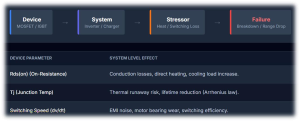
Every EV reliability story starts at the device level. Choices around Si/SiC MOSFET design, IGBT technology, gate-driver strategies, packaging, and thermal paths determine switching losses, heat, and long-term stress in traction inverters and onboard chargers. Under Indian duty cycles
— high ambient temperatures, stop-go traffic, overloaded vehicles, and poor roads — those design decisions show up later as derating, efficiency loss, or outright failures.
The same applies to battery cells and BMS hardware: cell chemistry, form factor, and sensing strategies determine how accurately the system can “see” degradation or thermal risk. When this visibility is poor, fleets experience unexpected range drops, thermal events, and a costly pattern of warranty claims and field fixes.
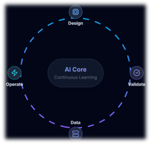
Traditional semiconductor and power-electronics design relies on simulations, design for reliability (DfR), lab validation, and field-return analysis. AI adds a new, continuous feedback loop: it learns from billions of switching events, thermal cycles, and usage profiles observed in real vehicles, and feeds that learning back into both device design and control algorithms.
This loop uses signals such as high-frequency waveforms, temperature gradients across modules, vibration signatures, and battery state-of-health (SoH) curves to identify stress patterns and precursors to failure. Over time, designers can co-optimize silicon, packaging, and firmware for actual Indian operating conditions rather than idealized lab scenarios — improving both first-time-right silicon and long-term field reliability.
A quick India scenario: Imagine a 2-wheeler fleet in Chennai. AI models trained on inverter waveforms and temperature data across thousands of rides can flag an emerging failure pattern in a particular batch of power modules and trigger an OTA-driven derating and firmware fix before riders see breakdowns.
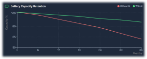
Four AI Capabilities That Change EV Reliability Predictive BMS Intelligence (Cell-level)Batteries are the single largest cost item in EVs and one of the most reliability-critical. AI models can continuously learn from cell voltages, temperatures, internal resistance evolution, and charge–discharge histories to detect early degradation, thermal runaway risk, and balancing drift at cell level. For Indian conditions — high temperatures, frequent partial charging, and stop-start usage — such predictive BMS intelligence can extend usable battery life by double-digit percentages and materially improve safety. Better SoH and range estimation also reduce range anxiety for drivers and allow fleet operators to plan maintenance proactively.
Traction inverters and motors sit at the heart of EV performance, directly built on semiconductor device and magnetic design Machine-learning models can analyse switching waveforms, current and voltage harmonics, torque–speed behavior, vibration patterns, and thermal maps to catch subtle anomalies long before a fault triggers a visible error. This enables early detection of gate-drive misbehavior, partial shorts, insulation degradation, bearing wear, and cooling issues that would otherwise surface as roadside failures or derated power. At fleet scale, such diagnostics can realistically cut unexpected drivetrain failures by 30–50%, significantly improving asset utilization.

Diagnostics alone are not enough; systems need a way to act on insights in the field. Over-the-air (OTA) firmware platforms, combined with AI, can detect abnormal behavior in ECUs, roll back to known-good images, patch vulnerabilities, and adjust control parameters to protect power devices and batteries. For example, if analytics indicate elevated stress on a particular inverter design in hot regions, OTA updates can modify switching patterns, current limits, or thermal thresholds to reduce risk without requiring a workshop visit. OEMs already see significant warranty and recall savings from OTA-based fixes; AI-guided self-healing will deepen this advantage and improve customer experience.

The full power of AI emerges when every vehicle becomes a data node. Connected EVs stream anonymized health, usage, and environment data to the cloud, where AI aggregates patterns across cities, duty cycles, and seasons. Refined diagnostic and control models are then pushed back to vehicles via OTA, closing the loop from chip to cloud and back.
In this paradigm, EVs do not just age; they improve over time. Updated BMS models provide better SoH estimates, inverter control becomes more efficient, and fault detection grows more sensitive with every kilometer driven. The same hardware platform becomes more valuable with each software and model refresh — a powerful shift in how the industry thinks about lifecycle value.

Evidence from other industries shows that AI-driven predictive maintenance can reduce unplanned downtime by about 30–50% and cut maintenance costs by 18–25% through earlier fault detection and better planning. At the same time, connected diagnostics and OTA capabilities allow OEMs to resolve many issues remotely, significantly lowering warranty and recall costs.
When these approaches are applied systematically across EV batteries, powertrain electronics, and software — and when semiconductor and system design are instrumented for rich telemetry — it is credible to target 40–60% improvements in reliability metrics and warranty economics over a multi-year horizon. This magnitude of impact justifies serious investment from OEMs, Tier-1s, Tier-2s, and policymakers.

- OEMs
- Define EV reliability KPIs (uptime, failure rates, cost per vehicle) that explicitly depend on electronics and AI, not just mechanical systems.
- Mandate data pipelines, OTA capabilities, and diagnostic hooks as core requirements in platform and supplier specifications.
- Tier-1 suppliers (inverters, BMS, ECUs, telematics)
- Design hardware and firmware with AI-grade observability: rich sensing, timestamped logs, and secure connectivity interfaces.
- Offer OEMs diagnostics and predictive-maintenance APIs as part of the product, not as optional add-ons.
- Tier-2 and component suppliers (devices, sensors, boards)
- Expose relevant device-level health signals (e.g., temperature, switching counters, error events) that higher-level ECUs and cloud models can consume.
- Collaborate with Tier-1s on test data, stress conditions, and failure signatures to make AI models more accurate.

India is already emerging as a major center for semiconductor design, verification, and R&D services, with global chip majors expanding their engineering presence in the country. Parallelly, the domestic EV market — particularly in 2-wheelers, 3-wheelers, and commercial fleets — is scaling rapidly, creating demanding real-world use cases that generate rich data for AI models.
This combination positions India to move beyond low-cost manufacturing and become a global hub for EV electronics intelligence, including:
- AI-optimized power device reference designs for SiC/IGBT
- Predictive and interpretable BMS/Inverter control
- Validated OTA/diagnostics platforms for fleet
These are exportable IP and platform plays that can serve global OEMs, not just domestic brands, while also anchoring higher-value electronics manufacturing within India.

To capture this opportunity, India’s ecosystem needs alignment across six pillars:
- Semiconductor & power-device design: Build AI-ready telemetry and reliability sensing into devices and modules from the outset.
- Power-electronics & system integration: Architect inverters, BMS, and ECUs for rich observability and secure connectivity.
- Software-defined vehicle architectures: Treat data collection, model deployment, and OTA as first-class design goals, not afterthoughts.
- Secure-by-design engineering: Ensure that telematics, OTA, and data flows are robust against cyber threats.
- Validation & standards: Extend traditional validation with AI-driven test generation, digital twins, and continuous in-field learning loops.
- Interdisciplinary Talent Development: Fund research and training programs to explicitly create hybrid talent (e.g., AI engineers specializing in power electronics and thermal physics) required to bridge the gap between device design and fleet data.
If OEMs, Tier-1s, Tier-2s, chip companies, startups, and policymakers work together across these pillars, India can define the template for AI-powered semiconductor design and EV reliability — and, in doing so, help lead the next global electronics revolution.

Email: mailsukhendu@gmail.com
LinkedIn: Sukhendu Deb Roy
The post AI-Powered Semiconductor Design for EV Reliability: Why India Can Lead the Next Electronics Revolution? appeared first on ELE Times.
UK and Canada collaborate on optical engine for faster, more efficient and more sustainable AI data centers
Kyocera and Rohde & Schwarz’s multipurpose phased array antenna module (PAAM) at CES 2026
Kyocera and Rohde & Schwarz will demonstrate the characterization of Kyocera’s novel phased array antenna module (PAAM) at CES 2026 in Las Vegas, NV. The demonstration at the Kyocera booth will feature the R&S ATS1800M 5G NR multi-directional mmWave test chamber from Rohde & Schwarz, known for its exceptionally small footprint and over-the-air (OTA) testing capabilities.
Kyocera has developed a novel phased array antenna module (PAAM) for a variety of sensing and communications applications. Featuring 384 dual-polarization elements, the PAAM can create up to eight simultaneous beams with varying directions and frequencies. This design incorporates 6G ISAC (Integrated Sensing and Communication) technology that combines wireless communication and sensing into a single framework. It allows networks to simultaneously deliver data and sense their environment, unlocking applications such as next-generation autonomous driving, environmental sensing, and industrial automation – all with greater efficiency and performance.
Ensuring all antenna elements work cohesively to form an RF beam with the desired characteristics is critical. Rohde & Schwarz offers a patented over-the-air (OTA) testing approach within a fully shielded environment, allowing engineers to verify beam patterns and minimize sidelobes.
The R&S ATS1800M is a unique solution featuring four feed antennas and CATR reflectors, each providing a 30 cm quiet zone (QZ). At CES 2026, the Kyocera PAAM device under test (DUT) will be positioned on a rugged 3D positioner at the center of the four overlapping QZs. This configuration allows Kyocera’s engineers to conduct a variety of tests, including the simultaneous reception of RF beams from multiple directions. The patented vertical CATR design minimizes the system’s lab footprint compared to other OTA solutions.
The complete test setup incorporates multiple instruments from Rohde & Schwarz, including signal generators and analyzers alongside the mmWave test chamber, providing a fully integrated testing environment. The device under test receives four independent signals via the chamber’s reflectors, simulating complex reception scenarios, and the resulting signal quality is measured and analyzed. This comprehensive system enables thorough evaluation of the phased array antenna module’s performance in realistic conditions.
Visitors to CES 2026 can experience this milestone demonstration live at the Kyocera booth (6501) in the West Hall of the Las Vegas Convention Center, from January 6 to 9, 2026.
The post Kyocera and Rohde & Schwarz’s multipurpose phased array antenna module (PAAM) at CES 2026 appeared first on ELE Times.
AI PCs: What Tata Electronics and Intel Aim to Scale in India
Tata Electronics, a global enterprise headquartered in India, and Intel Corporation, a US-based manufacturer of advanced semiconductors, have announced a strategic alliance to explore manufacturing and packaging of Intel products for the Indian Market at Tata’s upcoming Fab and OSAT plants. As part of the same MoU, the partnership between the companies also intends to scale up tailored AI PC solutions for consumer and enterprise markets in India. The AI PC market is expected to be one of the Global top 5 markets by 2030.
But what exactly is an AI PC?
An AI PC is a computer with a dedicated Neural Processing Unit (NPU) that renders unflinching reliability and speed to the AI processes over a PC. Such PCs can run large AI models locally as they are not heavily dependent on the cloud for functioning.
What is a Neural Processing Unit (NPU)?
A Neural Processing Unit (NPU) is a low-power yet dedicated chip installed only for AI/ML workloads. It consumes 10-20 percent less power as compared to conventional GPUs. It can efficiently handle everything from real-time language translation and speech-to-text to advanced vision tasks, and even the functions of a personal AI assistant.
Enhanced Security & Privacy
In Such PCs, local NPU-based AI execution ensures that private data remains on the system, minimizing cloud dependency and elevating overall security and confidentiality. It also excels in managing system resources intelligently for better performance and battery life.
Intel-Tata Collaboration
This collaboration would leverage Intel’s AI compute reference designs, Tata Electronics’ industry-leading Electronics Manufacturing Services (EMS) capabilities, and broad access to the Indian market through Tata Group companies. This collaboration marks a pivotal step towards developing an India-based geo-resilient electronics and semiconductor supply chain.
N Chandrasekaran, Chairman, Tata Sons, said, “The Tata Group is deeply committed to developing a robust semiconductor industry in India. We are excited to collaborate with Intel, and this strategic alliance would accelerate our efforts. Together, we will drive an expanded technology ecosystem and deliver leading semiconductors and systems solutions, positioning us well to capture the large and growing AI opportunity.”
The post AI PCs: What Tata Electronics and Intel Aim to Scale in India appeared first on ELE Times.
UP’s Semiconductor Push: State to Build Three New Electronics Hubs Beyond NCR
With an aim to boost development and employment beyond the traditional Noida-Greater Noida belt, the UP government is planning to set up three semiconductor hubs in the hinterland. The set up is expected to be established in Pilibhit, Barabanki, and Gorakhpur.
Government has strategically chosen these locations to tap local resources and improve connectivity in the region while reducing the pressure of over-urbanization in the western industrial region of the state. These three facilities will be part of the Electronics System Design and Manufacturing (ESDM) Initiative. The facilities are expected to attract private investment, generate skilled employment, and create a more balanced industrial demographic across the underdeveloped districts in the state.
Through this policy, Uttar Pradesh aims to become the prime state to fulfil the country’s electronic needs. It is already a key contributor of mobile manufacturing and other electronic components through facilities established in Noida and Greater Noida.
Anurag Yadav, Principal Secretary (IT and Electronics), said that UP is strengthening its position in the high-value electronics sector and attracting companies to set up operations. He confirmed that four anchor firms have already begun establishing their facilities.
The post UP’s Semiconductor Push: State to Build Three New Electronics Hubs Beyond NCR appeared first on ELE Times.
⛄ Святкові дні під час воєнного стану

Нагадуємо вам, що у період дії воєнного стану не застосовуються норми статті 53 (тривалість роботи напередодні святкових, неробочих і вихідних днів), частини першої статті 65, частин третьої – п’ятої статті 67 та статей 71,73,781 (святкові і неробочі дні) КЗпП України.
One Nation, One Compute Grid: India’s Leap into the AI and Supercomputing Era
Courtesy: Dr. Harilal Bhaskar, Chief Operating Officer (COO) and National Coordinator at I-STEM (Indian Science Technology and Engineering facilities Map) under the Office of Principal Scientific Adviser (P.S.A.) Government of India.
When Talent Meets Infrastructure
In a small university town in Bihar, a student dreams of designing renewable energy systems. She excels at theory and design, yet her laptop freezes during large-scale MATLAB simulations. In Andhra Pradesh, a doctoral scholar struggles to check her thesis against plagiarism databases because her institution lacks adequate licenses.
Meanwhile, across the world, peers in the United States, Europe, and China train artificial intelligence models on GPU clusters, run exascale climate simulations, and test quantum algorithms. The difference is not in talent—it is in infrastructure.
Innovation today is constrained not by ideas but by access to computing power. India’s researchers, start-ups, and students face uneven access to high-performance computing (HPC), AI platforms, and quantum resources. This gap threatens to widen inequality and slow national progress.
The Vision: A National Digital Commons
India’s answer is a federated national compute grid—a seamless network connecting supercomputers, AI labs, and emerging quantum facilities. Instead of duplicating procurement, ultra-expensive research platforms such as ANSYS Enterprise Suite, Dassault BIOVIA/SIMULIA, Schrödinger Drug Discovery, or quantum-grade simulation packages like VASP could be shared through centralized national licenses, reducing million-dollar expenditures while ensuring equitable access for researchers across domains.
Imagine the possibilities:
- A climate scientist in Assam running continental-scale simulations on a Bengaluru supercomputer.
- A linguist in Nagaland applying AI-powered text analytics without local infrastructure.
- A start-up in Pune experimenting with quantum testbeds via a national portal.
Such an ecosystem transforms access from privilege to commons, ensuring geography or budget does not decide opportunity.
Why Now: The Strategic Imperative
The global race for computational power is accelerating:
- United States: The NSF and Department of Energy provide access to some of the world’s fastest AI and supercomputing resources.
- European Union: The EuroHPC initiative builds exascale-ready systems while fostering cross-border collaboration.
- China: National HPC and quantum centres are aligned with industrial strategy and defence priorities.
India cannot afford fragmented approaches. A One Nation–One Compute Grid would unify HPC clusters, AI labs, quantum resources, and software licenses into a scalable, efficient national framework.
Current status underscores urgency: India’s most powerful system, PARAM Siddhi-AI, ranks only around 60th globally, far behind US and Chinese peers. Under the National Supercomputing Mission, 18 HPC systems have been deployed, but gaps remain in accessibility, GPUs, and quantum nodes. Without scale and coordination, India risks lagging behind in AI-driven innovation.
A National HPC–AI–Quantum Portal
Modern research in genomics, climate science, or AI requires resources far beyond individual labs. A National Compute Portal could:
- Catalogue available compute clusters, GPUs, and quantum nodes.
- Provide automated scheduling for resource booking.
- Allow priority allocation for urgent national missions (pandemic modelling, energy transition).
- Embed AI-guided support for booking and troubleshooting.
- Supply policymakers with dashboards for monitoring usage, efficiency, and outcomes.
This portal would serve as the command centre of India’s scientific computing ecosystem.
Building Skills and Human Capital
Infrastructure without skilled manpower risks underutilization. Alongside the portal, India must:
- Expand HPC/AI training programs in IITs, NITs, and universities.
- Develop quantum algorithm bootcamps for researchers and start-ups.
- Create national fellowships for AI-HPC specialists to ensure talent pipelines.
This ensures that the grid is not just available, but also actively and effectively used.
AI Labs, Industry Integration, and Regional Balance
HPC thrives when connected to broader ecosystems:
- Start-ups can test AI or quantum algorithms without heavy capital costs.
- Universities and national labs can pool datasets and compute power.
- Sector-specific labs—in health, climate, finance, cybersecurity—can run experiments at scale with real-world impact.
Equity must be central:
- Tier-2 and Tier-3 cities should gain equal access through the portal.
- Incentives must support rural and state universities, ensuring inclusion beyond elite IIT/IISc clusters.
Here, HPC and AI infrastructure are the engines, while software serves as a supporting layer.
Governance, Security, and Funding Models
A unified system requires layered governance:
- Central Government: anchor investments, negotiate national licenses, and set mission priorities.
- Institutions: contribute idle compute cycles and avoid duplication.
- Industry and CSR programmes: co-invest in AI accelerators, GPUs, and quantum nodes.
- Oversight: embed cybersecurity, fair-use policies, and ethical AI standards.
Security and sovereignty must be priorities:
- Strong encryption and access controls.
- Safeguards for genomic, financial, and citizen datasets.
- Alignment with India’s Digital Personal Data Protection Act (DPDPA, 2023).
Funding pathways could include:
- Public–private partnerships for data centres.
- Corporate CSR support for compute nodes.
- A “compute credit” model, where researchers and start-ups receive national cloud-like credits.
Learning from Global Models
- United States: Federated HPC networks maximize scale and reach.
- European Union: Cross-border HPC integration builds resilience and efficiency.
- China: Strategic placement of HPC and quantum centres accelerates industrial outcomes.
India can draw from all three—combining scale, inclusivity, and strategic alignment—into one unified ecosystem.
Sustainability and Green Computing
HPC centres are energy-intensive. To align with India’s climate commitments, the grid should:
- Use renewable-powered data centres.
- Incentivize energy-efficient GPUs and low-carbon quantum hardware.
- Deploy AI to optimize energy scheduling and cooling.
This ensures that innovation does not come at the cost of sustainability.
Global Collaboration
A national compute grid strengthens India’s role in global alliances:
- Participation in BRICS quantum/HPC research.
- Collaborations with the QUAD on AI standards.
- Bilateral HPC/quantum projects with partners like Japan, US, and EU.
India’s unified grid would make it a preferred partner in global science and innovation diplomacy.
The Payoff: Democratization and Innovation
A One Nation–One Compute Grid would:
- Democratize access to HPC, AI, and quantum platforms.
- Accelerate patents, research output, and industrial prototypes.
- Strengthen academic integrity with AI-powered plagiarism detection.
- Optimize the National Supercomputing Mission and quantum initiatives.
- Cut redundant spending on licenses and infrastructure.
- Empower start-ups, SMEs, and industry to innovate at scale.
- Ensure balanced regional development and global competitiveness.
The outcome is a knowledge republic, where innovation flows from ideas—not from institutional budgets or geography.
Conclusion: Building the Knowledge Republic
India has already transformed governance and finance with Aadhaar and UPI. The next frontier is research infrastructure.
A One Nation–One Compute Grid—anchored in HPC, AI labs, and quantum computing, and strengthened by shared software, skilled manpower, and green sustainability—can redefine India’s place in global innovation.
The real question is not whether India can build this system.
The question is: Can India afford not to?
The post One Nation, One Compute Grid: India’s Leap into the AI and Supercomputing Era appeared first on ELE Times.
CEA-Leti & STMicroelectronics’ Demonstrate Path to Fully Monolithic Silicon RF Front-Ends with 3D Sequential Integration at IEDM 2025
CEA-Leti and STMicroelectronics showcased key enablers for a new high-performance and versatile RF Si platform cointegrating best-in-class active and passive devices used in RF and Optical FEM at IEDM 2025. Their paper detailed 3D sequential integration of silicon-germanium (SiGe) heterojunction bipolar transistors (HBT), RF SOI switches, and high-quality passives on a single wafer—opening a path to highly integrated, low parasitic, and targeting cost-efficient systems for next-generation wireless and wireline communications.
The paper, “Unlocking High-Performance Si RF Platforms with SiGe HBT and RFSOI Switch Technologies,” described the methodology to directly build high-performance components on the same silicon wafer rather than packaged or stacked as separate chips. This can be achieved through 3D sequential integration, which layers different device types, such as SiGe HBT and SOI CMOS switches, without overheating the lower tiers during processing.
‘Efficient and Cost-Effective’
“Our team has shown that high-performance SiGe HBT has been conceived to be compatible with the top-tier fabrication steps, and that trap-rich isolation can be localized and thermally robust, and low-temperature (600°C) SOI switches can match state-of-the-art figures of merits,” said CEA-Leti’s Thibaud Fache, lead author of the paper. “These results pave the way to an all-silicon RF front-end module that is efficient and cost-effective.”
The team showed that a localized trap rich layer can achieve RF isolation and linearity comparable to costly commercial trap-rich substrates, while withstanding thermal cycles up to 600 °C—preserving the performance of the underlying SiGe HBT layer.
‘From Advanced Research to Manufacturable Solutions’
By extending silicon’s reach of sequential integration into the RF domain, the CEA-Leti/ST team’s work points to a future of more accessible, energy-efficient connectivity. Fully integrated RF and optical front ends could simplify the manufacturing and enable cost-effective deployment of dense wireless networks essential for smart cities, autonomous systems, and AI datacenters.
“This joint result demonstrates a credible path from advanced research to manufacturable solutions,” said ST’s Thomas Bordignon, co-author of the paper. “By combining CEA-Leti’s sequential integration know-how with ST’s RF technology expertise, we’re enabling the co-integration of state-of-the-art SiGe HBT, switches and passive devices, that are key elements of the FEM.”
Materials Science Milestone
Achieving a performant RF Partially Depleted (PD) SOI switch at 600 °C rather than standard ~1000 °C is a first. It is worth noting that process flow of this low-temperature device does not rely on new equipment or costly steps and is thus quickly industrially viable thanks to the relatively relaxed thermal budget constraints of bottom tier (600°C). The team demonstrated high-quality, low-loss RF switches fabricated at 600 °C, maintaining the performance of the SiGe HBT below and confirming the feasibility of a fully integrated silicon RF platform.
Additional Breakthrough Presentation
CEA-Leti researchers will report tomorrow a major breakthrough (session 33-4) with the design of high-performance silicon-on-insulator (SOI) MOSFETs processed at 400°C. NMOS and pMOS transistors demonstrate state-of-the art performances among the Back-End-Of-Line devices, fulfilling all industrial figures of merit without any compromise. This reliable versatile analog transistor targets More Than Moore applications bringing differential advantage for smart sensors, near memory computing and RF devices.
The post CEA-Leti & STMicroelectronics’ Demonstrate Path to Fully Monolithic Silicon RF Front-Ends with 3D Sequential Integration at IEDM 2025 appeared first on ELE Times.
New, Imaginative AI-enabled satellite applications through Spacechips
As the demand for smaller satellites with sophisticated computational capabilities and reliable along with robust onboard processor systems to support the five to ten-year duration of a mission grows, so does the limits of the latest ultra‑deep‑submicron FPGAs and ASICs and their power delivery networks. These high-performance processors have demanding, low-voltage, high-current power requirements and their system design is further compounded by the complexities of managing thermal and radiation conditions in space.
To cater to these demands, Spacechips has introduced its AI1 transponder, a small, on-board processor card containing an ACAP (Adaptive Compute Acceleration Platform) AI accelerator. The smart, re-configurable receiver and transmitter delivers up to 133 tera operations per second (TOPS) of performance that enables new Earth-observation, in-space servicing, assembly and manufacturing (ISAM), signals intelligence (SIGINT), and intelligence, surveillance and reconnaissance (ISR) and telecommunication applications to support real-time, autonomous computing while ensuring the reliability and longevity to complete longer missions.
“Many spacecraft operators simply don’t have sufficient bandwidth in the RF spectrum to download all of the data they’ve acquired for real-time processing,” said Dr. Rajan Bedi, CEO of Spacechips. “An alternative solution is accomplishing the processing in-orbit and simply downlink the intelligent insights.”
New levels of processing power spawn imaginative new applications in space and on Earth
Today’s low-Earth-orbit observation spacecraft can establish direct line of sight over a specific region only about once every ten minutes. If satellites were trained to fill those blind spots using AI algorithms, emergency management teams could make faster, better-informed decisions when direct line-of-sight communication with Earth is not possible. Spacechips is harnessing these powerful artificial intelligence compute engines to enable in-orbit AI to address a variety of Earth-bound and space-related problems:
- Tracking space debris to avoid costly collisions
- Monitoring mission critical spacecraft system health
- Identifying severe weather patterns
- Reporting critical crop production rainfall data
 Figure 1 On-orbit AI can detect temperature anomalies such as wildfires, volcanic activity, or industrial accidents with the Spacechips AI1 processer. This helps emergency management teams make faster, better-informed decisions about which fire prone areas are the most vulnerable.
Vicor Factorized Power Architecture delivers high current, low voltage
Given the constrained operating environment of space, AI-enabled computing has an acute need for precision power management. The need is compounded by the expanding number, scope and variety of missions that require different kinds of spacecraft and a growing reliance on some form of solar power to deliver adequate power.
This led Spacechips to partner with Vicor to incorporate Vicor Factorized Power Architecture (FPA) using high density power modules into the Spacechips AI1 Transponder Board. FPA is a power delivery system design that separates the functions of DC-DC conversion into independent modules. In Vicor’s radiation tolerant modules, the bus converter module (BCM) provides the isolation and step down to 28V, while the pre-regulator module (PRM) provides regulation to a voltage transformation module (VTM) or current multiplier that performs the 28V DC transformation to 0.8V.
The value of the Vicor solution, according to Bedi, is that it is very small and power dense. This allows for better efficiency and flexibility by reducing size and weight and yields higher power density, especially in high-performance computing applications.
By adopting Vicor’s FPA power delivery system, Bedi is helping telecommunications and SIGINT operators perform real-time, on-board processing by autonomously changing RF frequency plans, channelization, modulation and communication standards based on live traffic needs. Vicor power converter modules also feature a dual powertrain, which for fault-intolerant space applications provides built-in redundancy that allows loads to be driven at 100 percent on each side of the powertrain.
 Figure 2 Vicor Factorized Power Architecture (FPA) separates the functions of DC-DC conversion into independent modules. Using radiation-tolerant modules, the BCM bus converter provides the isolation, the PRM regulator provides the regulation and the VTM current multiplier performs the DC transformation. This allows for better efficiency, flexibility and higher power density, especially in high-performance computing applications.
“Vicor FPA delivers a much more elegant, efficient solution in a very small form factor,” Bedi said. “The benefits of Vicor FPA are simply an order of magnitude superior to everything else on the market.”
Together Spacechips and Vicor have partnered to design the most power-dense, reliable processer board on orbit. The AI1 board is rad-tolerant, rugged and compact. It sets a new standard for power processing, enabling the next-generation of computing and application design for New Space.
The post New, Imaginative AI-enabled satellite applications through Spacechips appeared first on ELE Times.
Fighting Fire with Fire: How AI is Tackling Its Own Energy Consumption Challenge to Boost Supply Chain Resilience
AI is no longer just a futuristic idea, today it is a known technology across every industry. AI is being used to automate tasks, make quicker decisions, and build digital products that were once considered impossible to create. But as AI becomes more common, a major problem is starting to show up: it uses a lot of energy. Training large models and keeping them running day and night requires huge amounts of computing power, which in turn puts pressure on power grids, data centres, and the supply chains that support them.
This creates a clear paradox. AI demands significant energy, yet it can also help organisations manage energy more efficiently. With data centre power requirements expected to rise sharply, procurement teams, engineers, and supply chain leaders must reconsider how AI systems are designed, deployed, and supported. Encouragingly, low-power AI architectures and smarter data-centre management tools are emerging to tackle the issue from within the ecosystem.
Energy Consumption Profile of AI Technologies
AI’s energy demand has surged as newer models grow larger and more compute-intensive. Boston Consulting Group reports that U.S. data centers consumed about 2.5% of national electricity in 2022, a share projected to rise to nearly 7.5% around 390 TWh by 2030.
The biggest contributors include:
- Model Training
Training today’s large models isn’t a simple overnight job. It involves running thousands of GPUs or specialised AI chips in parallel for weeks at a stretch. The compute load is enormous, and the cooling systems have to run constantly just to stop the hardware from overheating. Together, they draw a surprising amount of power.
- Data Center Operations
People often assume most of the power goes into the servers, but the cooling and air-handling equipment consume almost as much. As AI traffic grows, data centers are forced to maintain tight temperature and latency requirements, which makes the power bill climb even faster.
- Inference at Scale
Running models in real time, or inference, now accounts for most of AI’s total energy consumption. With generative AI being used in search engines, content creation tools, manufacturing systems, and supply chain operations, continuous inference tasks place constant pressure on electricity infrastructure.
AI-Driven Strategies for Energy EfficiencyTo mitigate AI’s energy consumption, several AI-driven strategies have been developed:
- Energy-Efficient Model Architectures
Modern AI research increasingly focuses on architectures that deliver higher performance with lower computational load. Techniques gaining wide adoption include:
- Pruning: Removing redundant neurons and parameters to shrink model size.
- Quantization: Reducing precision (e.g., FP32 → INT8) with minimal accuracy loss.
- Knowledge Distillation: Compressing large teacher models into compact student models.
These approaches can cut training and inference energy by 30–60%, making them critical for enterprise-scale deployments.
- Adaptive Training Methods
Adaptive training methods dynamically adjust GPU allocation, batch size, and learning rate based on convergence behavior. Instead of running training jobs at maximum power regardless of need, compute intensity scales intelligently. This prevents over-provisioning, lowers operational costs, and reduces carbon footprint particularly in cloud-based AI development workflows.
- AI-Powered Data Center Energy Management
AI is increasingly being integrated into Hyperscale data-centre control systems because it can monitor operations faster than humans. It tracks power usage, detects irregularities, and predicts demand spikes so workloads and cooling can be adjusted before issues arise.
Google applied this approach in its facilities and found that machine-learning–based cooling adjustments reduced energy use by about 15–20%. According to Urs Hölzle, this improvement came from predicting load changes and tuning cooling in advance.
- Cooling System Optimization
Cooling is one of the largest energy loads in data centres. AI-driven cooling systems, especially those using offline reinforcement learning, have achieved 14–21% energy savings while maintaining thermal stability.
Techniques include:
- Predicting thermal hotspots
- Dynamic airflow and coolant modulation
- Intelligent chiller sequencing
- Liquid-cooled rack optimization
As AI model density increases, these innovations are essential for maintaining operational uptime.
- Predictive Analytics for Lead Time Optimization
AI forecasting tools optimize procurement, lead time, and logistics by predicting:
- Seasonal energy price fluctuations
- Grid availability
- Renewable energy generation patterns
- Peak demand windows
These insights allow organizations to schedule compute-heavy workloads like model training-during low-cost or low-emission energy periods, directly improving supply chain resilience
Strategic Implications for Procurement and Supply Chain ManagementEnergy-efficient AI is not merely an IT requirement; it is a supply chain strategy. Organizations are rethinking how they source hardware, design workflows, and plan operations.
1. Procurement of Energy-Efficient Semiconductors
The demand for low-power AI accelerators and CPUs-such as Arm Neoverse platforms is rising sharply. Procurement leaders must prioritize vendors who offer:
- High performance-per-watt
- Advanced power management features
- Hardware-level AI acceleration
Selecting the right semiconductor partners reduces long-term operational costs and aligns with sustainability commitments
- Enhancing Supply Chain Resilience
Energy availability and cost volatility can trigger delays, downtime, and disruptions. AI-based energy optimization enhances resilience by:
- Predicting shortages
- Reducing load on critical systems
- Identifying alternative low-power workflows
- Optimizing backup generation or renewable energy use
This is particularly vital for semiconductor fabs, logistics hubs, and manufacturing plants that rely on uninterrupted power.
- Wafer Fab Scheduling Analogies
The semiconductor industry offers a useful analogy: wafer fabrication requires meticulous scheduling to optimize throughput while managing energy-intensive processes. AI-driven energy management requires:
- Workload balancing
- Thermal and power constraint management
- Predictive scheduling
- Minimization of idle compute cycles
Several trends are shaping the next wave of AI energy innovation:
1. Specialized Low-Power AI Chips
Arm, NVIDIA, AMD, and start-ups are designing AI chips focused on maximum efficiency per watt-critical for both data centers and edge AI systems.
2. Green Data Centers
Operators are investing in:
- Renewable power
- Liquid immersion cooling
- Waste heat reuse
- Modular micro-data centers
These reduce operational emissions and increase grid independence.
3. Regulatory Pressures
Governments are introducing stricter carbon reporting, energy consumption caps, and sustainability requirements—pushing organizations toward greener AI adoption.
4. Market Volatility
Energy price fluctuations directly impact the cost of training and deploying AI. Organizations must adopt agile, energy-aware planning to maintain competitiveness.
ConclusionAI is in a strange position right now. On one hand, it consumes a huge amount of energy; on the other, it’s one of the best tools we have for cutting energy waste. When companies use more efficient model designs, smarter data-center management systems, and predictive tools that anticipate resource needs, they can bring down operating costs and make their supply chains more stable.
Using sustainable AI isn’t just a “good to have” anymore it’s becoming a key factor in staying competitive. As businesses push deeper into digital operations, the combination of AI innovation and energy-conscious thinking will play a major role in determining which organisations stay resilient and which ones fall behind.
The post Fighting Fire with Fire: How AI is Tackling Its Own Energy Consumption Challenge to Boost Supply Chain Resilience appeared first on ELE Times.
Beyond the Bill: How AI-Enabled Smart Meters Are Driving Lead Time Optimization and Supply Chain Resilience in the Energy Grid
Introduction
Smart meters have significantly evolved since their initial implementation for consumer billing. In the contemporary networked industrial landscape, where semiconductor fabrication facilities, data centers, and manufacturing plants rely on a consistent, high-quality electrical supply, AI-enabled smart meters have become essential instruments. These meters, integrated with edge analytics, IoT infrastructures, and cloud-based machine learning engines, produce high-resolution data that informs procurement, operational planning, and supply chain resilience.
For the semiconductor industry, where a single hour of downtime in a wafer fab can cost between $1–5 million, energy reliability is not merely operational, it is existential. By using predictive analytics from AI-enabled smart meters, both utilities and semiconductor fabs gain visibility into consumption anomalies, voltage instability, and equipment stress patterns that traditionally led to delays, yield losses, and unplanned shutdowns.
As Dr. Aaron Shields, Director of Grid Strategy at VoltEdge, remarks-For semiconductor fabs, energy intelligence is no different from process intelligence. AI-enabled metering is now a supply chain stabilizer, not just a measurement tool.
Smart Meters as Intelligent, High-Resolution Energy Nodes
Smart Meters as Sophisticated, High-Resolution Energy Nodes
Contemporary AI-driven smart meters possess integrated processors, edge AI chips, and secure communication protocols. These qualities convert them into “micro-decision engines” capable of executing:
- Local anomaly detection
- High-frequency load forecasting
- Voltage quality assessment
- DER coordination
- Event-driven grid signalling
This is especially important for semiconductor ecosystems, which need very careful monitoring because they are very sensitive to voltage drops, harmonics, and micro-interruptions.
Semiconductor fabs typically run:
- 5,000–50,000 process tools,
- under strict schedule windows,
- where wafer fab scheduling depends on consistent energy flow to keep lithography, etching, CMP, and deposition tools stable.
AI-enabled smart meters supply real-time, tool-level and grid-level data that feeds these scheduling algorithms, reducing cycle time disruptions.
AI Applications for Grid Optimization and Semiconductor Supply Chain Stability
Through a number of methods, AI-enabled smart meters improve supply chain resilience in the utility and semiconductor manufacturing industries.
Predictive Maintenance & Equipment Lead Time Planning
AI detects early signatures of:
- transformer fatigue,
- feeder overloads,
- harmonic distortions,
- and breaker stress.
Utilities can then predict how many spare parts they will need and speed up the delivery of important parts. Semiconductor fabs likewise gain advance warning for facility equipment—HVAC loads, chillers, pumps, and vacuum systems.
Demand Forecasting with Industry-Specific Models
AI models like LSTM, transformer networks, and hybrid ARIMA-ML pipelines look at things like:
- Patterns in the production cycle
- Peak fab energy windows
- Changes in seasonal demand
- Large tool starts up currents
- Changes in the grid at the level of the grid
Better energy forecasting helps fab procurement leaders get power contracts, make better energy-based costing models, and cut down on delays caused by volatility.
Risk Mitigation During Market Volatility
Changes in energy prices have a direct effect on the costs of making chips. AI-AI-driven intelligent metering offers:
- Early warnings of grid instability
- Risk maps highlighting feeders that could trigger fab downtime
- Real-time dashboards for emergency preparedness
This improves the stability of the semiconductor supply chain amid energy price volatility or grid congestion events..
Case Study 1: European Utility + Semiconductor Fab Partnership Reduces Lead Times by 28%
A prominent European utility implemented AI-integrated smart meters throughout the industrial area containing a semiconductor fabrication facility with a capacity of 300,000 wafers per month. Historically, unpredictable transformer failures forced the fab to activate emergency procurement workflows.
AI-driven meter analytics identified transformer strain 18 days prior to conventional SCADA systems
This gave the utility’s purchasing team the ability to:
- Reorder transformer modules ahead of time
- Reduce urgent shipment costs
- Avoid fab shutdowns
Result:
- 28% reduction in transformer component lead times
- Zero unplanned fab downtime in eight months
- 12% improvement in wafer fab scheduling adherence
Case Study 2: Indian Fab Achieves 22% Faster Spare-Part Fulfilment Using Smart Meter Predictive Analytics
AI-enabled smart meters were installed from substation to tool-level feeders at a semiconductor fab park in India. Unusual starting-current spikes in the CMP and deposition sections were detected by predictive analytics, suggesting impending breaker degradation.
The fabs supply chain leaders integrated this data into their ERP procurement engine.
Impact:
- Spare-part availability increased by 24%
- Maintenance response times improved by 22%
- Downtime during voltage sag occurrences lowered by 17%%
The park’s engineering head noted: “Intelligence from smart meters now directs our procurement schedule.” We strategize weeks in advance, rather than hours.
Strategic Insights for Procurement Leaders Across Energy & Semiconductor Sectors
- Granular consumption data facilitates precise procurement. Prediction Meter data facilitates the prediction of:
Meter data helps forecast:
- Spare-transformer needs
- HVAC load cycles
- Cleanroom energy peaks
- Fuel windows for backup generators
This facilitates long-term vendor agreements and minimizes unanticipated orders.
- Smarter Vendor Evaluation
Tool uptime and voltage stability data allow semiconductor fabs to evaluate how supplier components behave under real load conditions.
- Lead Time Optimization Through Predictive Insights
Early detection of energy-side failures prevents:
- Wafer batches that are late,
- Cycle times that are too long, and
- Tool requalification delays.
Utility supply chains also reduce buffer stocks while improving availability.
- Operational Resilience and Risk Mitigation
AI-enabled data supports:
- Contingency planning
- Load re-routing
- Rapid DER activation
- Process tool safeguarding
This is crucial in a sector where milliseconds of voltage fluctuation can scrap millions in wafers.
Future Trends: Where Energy Intelligence Meets Semiconductor Precision
- AI-Orchestrated Load Scheduling for Fabs
Predictive models will align fab tool scheduling with energy stability windows. - Digital Twins Using Smart Meter Data
Utilities and fabs will run simulations to test equipment stress scenarios before making procurement decisions. - Edge AI Advancements
Next-generation meters will host larger models that independently diagnose harmonic distortions critical to lithography and etching tools. - Real-Time ROI Dashboards
CFOs in the semiconductor sector will see energy risk reduction as a way to get a good return on investment.
Conclusion
Artificial intelligence-enabled smart meters are essential for the modernization of the electricity grid and the stabilization of the semiconductor supply chain. Procurement directors, supply chain strategists, and fabrication engineers can make informed, proactive decisions with access to real-time analytics, predictive maintenance metrics, and load forecasting information. Smart meters are increasingly essential for maintaining production schedules, reducing lead times, and remaining competitive globally, as wafer manufacture requires consistent, high-quality power.
The post Beyond the Bill: How AI-Enabled Smart Meters Are Driving Lead Time Optimization and Supply Chain Resilience in the Energy Grid appeared first on ELE Times.
Inside the Digital Twin: How AI is Building Virtual Fabs to Prevent Trillion-Dollar Mistakes
Introduction
Semiconductor manufacturing often feels like modern alchemy: billions of tiny transistors squeezed onto a chip smaller than a fingernail, stitched through thousands of precise steps. Shifting a line by nanometres can ruin the batch.
The stakes are enormous. One day of unplanned downtime in a top fab can wipe out over $20 million. Problems aren’t always dramatic shutdowns; sometimes, process drift quietly eats into yields, totalling billions in lost revenue yearly. Factor in easily wobbling supply chains, and you see the industry’s looming “trillion-dollar risk.”
AI-powered digital twins are living mirrors of the factory. Continuously updated with real data, they run endless “what-if” scenarios, catching errors before they become costly. It’s like rehearsing production virtually, avoiding real-world mistakes.
- What is a Digital Twin in Semiconductor Manufacturing?
Now, a digital twin in a fab isn’t just some fancy simulation it’s basically a virtual twin of the whole facility, kept in lockstep with the real thing. Traditional simulations? They’re kind of frozen in time. Digital twins, on the other hand, are always moving, always learning, pulling in data from thousands of sensors, tool logs, and manufacturing systems to really reflect what’s happening on the floor.
Their scope is huge. For instance:
- Wafer Fab Scheduling: Figuring out the best sequence and queue times across hundreds of tools, shaving days off wafer cycles that can otherwise drag past 90 days.
- Tool Behavior Simulation: Watching how lithography, etching, and deposition tools drift or wear out, and guessing when they’ll need attention.
- Predictive Maintenance: Catching potential failures before they hit, avoiding downtime that could grind production to a halt.
The cool part? They keep getting smarter. Every wafer that runs through the fab teaches the twin a little more, helping it predict better and suggest fixes before things go sideways. Over time, fabs move from constantly reacting to actually staying ahead of the game.
- How AI Makes Digital Twins Smarter
AI is the real power that changes things. Digital twins transition from mere reflections to autonomous control systems capable of independent decision-making.
For instance:
- Defect Prediction: Machine learning spots tiny defect patterns humans or simple rules miss. A lithography misalignment, for instance, is caught before it ruins wafers.
- Automated Calibration: Reinforcement learning algorithms fine-tune deposition or etch times, keeping precision high with minimal human input.
- Fab Simulation: You can stress-test entire fabs virtually (temperature, vibration, purity changes) to see how production fares.
The impact is real:
- 30% faster validation, qualifying new processes quicker.
- 25% better yield forecasts, cutting waste.
- Avoided downtime over $2 million per tool daily (SEMI data).
AI tools like Bayesian models and reinforcement learning push fabs toward self-regulation—the factory learns to heal itself. The workflow below shows how AI twins turn raw data into better supply chain outcomes.

Figure 1: AI-powered digital twins connect fab data, predictive analytics, and real-time simulation to deliver measurable gains in yield, procurement efficiency, and supply chain resilience.
- Procurement & Supply Chain Resilience
The engineering benefits of digital twins are clear, but they also bring unexpected value to procurement and supply chain planning, functions exposed as fragile during the pandemic-era chip shortage.
- Supplier Qualification: Before approving new photoresists, gases, or wafers, digital twins simulate their impact on yield, reducing the risk of supplier-induced disruptions.
- Equipment Sourcing: AI predicts the saturation point of tools, enabling fabs to place orders in advance and avoid expensive overstocking.
- Virtual Commissioning: Tools can be simulated in the digital twin prior to acquisition, guaranteeing return on investment and compatibility with current production lines.
Case Study: When advanced lithography tools ran short in 2021, a major foundry used its twin to re-sequence wafer queues. This move held throughput steady, saved nearly $5 million in delay costs, and kept chips on schedule.
The globalization of supply chains necessitates this foresight. A firm in Taiwan can now anticipate the effects of a European chemical delay weeks in advance and adjust wafer production schedules to mitigate losses.
- Future Outlook: Virtual Fabs, Resilience, and ESG
The goal is the “virtual-first fab.” Every new process or recipe must be fully tested in the twin before going live. That method sharply lowers risk and cuts the cost of old-school trial-and-error.
Beyond efficiency, twins are crucial for sustainability targets:
- Scrap: Less wafer loss helps factories cut material scrap by 5–10%.
- Energy: Better tuning and scheduling can drop energy use by 3–7% per wafer.
- Waste: Fewer reworks directly cuts chemical and water usage.
Rahimian and other experts say that smart fabs of the future will combine efficiency with resilience, making supply chains stronger and better for the environment.
- Challenges on the Road Ahead
Despite their promise, setting up and maintaining a digital twin system is tough.
- Data Silos: Merging data from specialized, unlike tools is the core issue. Many factories use older equipment that lacks common data formats.
- Computational Demands: Running high-fidelity twins needs exascale computing, which smaller operations can’t afford.
- Adoption Hurdles: The industry needs simple rules for interoperability. Plus, veteran engineers must trust AI over their experience.
Solving this requires equipment makers, software firms, and chip producers to collaborate. Groups like SEMI are already pushing for common standards.
- Visualizing the Future
To see the full potential, think of a digital dashboard for a modern fab operator:
A heatmap shows when the wafer queue will be full, so there is no chaos. 3D models forecast tool wear weeks in advance. A supply chain radar tracks every bottleneck like a neon shortage or logistics delay in real time.
These visuals change factories from reactive spaces to proactive ecosystems. Every worker can now anticipate and adapt to changes, instead of constantly fighting crises.
Conclusion
The semiconductor industry drives nearly every modern device, yet its manufacturing risks are enormous. Digital twins are becoming essential because they let engineers spot yield problems early, see where supply issues may emerge, and keep sustainability efforts on track. These models aren’t just virtual copies of factories; they give teams clearer insight into how to run tools, materials, and workflows more efficiently and with fewer surprises. As digital-twin technology matures, it’s set to influence how leading fabs plan, test, and refine production. The message is clear: manufacturing’s future isn’t only physical. It’s virtual-first, AI-validated, and designed to prevent trillion-dollar mistakes.
The post Inside the Digital Twin: How AI is Building Virtual Fabs to Prevent Trillion-Dollar Mistakes appeared first on ELE Times.
ZK-DPL DC-DC Buck-Boost-Module
 | My little lovely ZK-DPL has arrived. It is adjustable DC-DC buck-boost power supply module featuring a digital display for output voltage/current, multiple input options (USB, Micro-USB, pads), and designed for stepping voltages up or down (e.g., 5V to 3.3V, 9V, 12V, 24V) at 3W max output. working aruond to find some cool things to do with it :) [link] [comments] |
Inductive sensor simplifies position sensing

Melexis introduces a 16-bit inductive sensor for robotics, industrial, and mobility applications. The new dual-input MLX90514 delivers absolute position with high noise immunity through its SSI output protocol.
Applications such as robotic joint control, industrial motor commutation, and e-mobility drive systems require sensors with high-precision feedback, compact form factor, low-latency response, resilience to environmental stressors, and seamless integration, Melexis explained.
These sensors also need to overcome the limitations of optical encoders and magnetic-based solutions, the company said, which the MLX90514 addresses with its contactless inductive measurement principle. This results in stable and repeatable performance in demanding operational environments.
The inductive measurement principle operates without a permanent magnet, reducing design effort, and the sensor’s PCB-based coil design simplifies assembly and reduces costs, Melexis added.
In addition, the sensor is robust against dust, mechanical wear, and contamination compared with optical solutions. The operating temperature ranges from ‐40°C to 160°C.
 (Source: Melexis)
The inductive sensor’s dual-input architecture simultaneously processes signals from two coil sets to compute vernier angles on-chip. This architecture consolidates position sensing in a single IC, reducing external circuitry and enhancing accuracy.
The MLX90514 also ensures synchronized measurements, and supports enhanced functional safety for applications such as measuring both input and output positions of a motor in e-bikes, motorcycles, or robotic joints, according to the company.
Targeting both absolute rotary or linear motion sensing, the MLX90514 provides up to 16-bit position resolution and zero-latency measurement with accuracy better than 0.1° for precise control in demanding environments. Other features include a 5-V supply voltage, coil diameters ranging from 20 mm to 300 mm, and linear displacements of up to 400 mm.
The inductive sensor offers plug-and-play configuration. Engineers only need to program a limited set of parameters, specifically offset compensation and linearization, for faster system integration.
The MLX90514 inductive sensor interface IC is available now. Melexis offers a free online Inductive Simulator tool, which allows users to design and optimize coil layouts for the MLX90514.
The post Inductive sensor simplifies position sensing appeared first on EDN.
Сторінки

