


Збирач потоків
How to make a simple low voltage dc power and data over 2 wires.
 | submitted by /u/Relevant_Pumpkin9190 [link] [comments] |
Navitas to acquire power management firm Claros
Flexible and Printed Electronics: The Circuits of the Future
3D-Printed Frame for a 32×32 LED Matrix with Microphone
GSM Emergency Call System with RF Receiver for Elderly and Bedridden Patients
Infineon Acquires C2i Semiconductors to Expand its Innovation Capabilities in AI Data Center Power Management Solutions
Infineon Technologies AG today announced the acquisition of C2i Semiconductors, a Bangalore-based technology company specializing in software-defined multiphase controllers and smart power stages for AI data center applications. C2i Semiconductors’ technology complements Infineon’s leading portfolio of power semiconductors and power systems, enabling intelligent and scalable power delivery architectures from grid to core for AI servers and high-performance computing platforms. The acquisition further strengthens Infineon’s top position in power solutions for AI data centers while expanding its engineering capabilities in India and reinforcing the country’s role as a strategic innovation hub. The transaction is expected to close in the third quarter of calendar year 2026.
“This acquisition will further strengthen Infineon’s leadership in power solutions for AI data centers and create a new center of excellence for digital power technologies in India,” said Adam White, President of Infineon’s Power Systems (PS) division. “C2i Semiconductors brings exceptional expertise in software-defined power management and system-level power architectures, backed by a proven highly experienced engineering team with decades of combined industry experience. With this acquisition, we will accelerate innovation in power delivery solutions for AI data centers, expand our capabilities in next-generation vertical power delivery architectures, and create significant value for our customers.”
“We founded C2i Semiconductors with the vision of bringing greater intelligence to power delivery systems and addressing the growing power challenges of AI infrastructure. Joining Infineon gives us access to world-class semiconductor technologies, manufacturing capabilities, and global customer relationships. Together, we can accelerate the development of software-defined power architectures and bring our innovations to customers worldwide,” says Ram Anant, Founder & CEO of C2i Semiconductors.
Software-defined power solutions combine advanced power semiconductors with intelligent digital control and software algorithms to optimize power conversion, regulation and system performance in real time. As increasingly powerful AI processors create highly dynamic and rapidly changing power demands, power delivery systems must respond faster and more precisely to sudden load fluctuations while maintaining efficiency and system stability. By adding intelligence to the power delivery architecture, software-defined solutions help data center operators improve efficiency, reduce power losses, and support the increasing power density requirements of next-generation AI processors. C2i Semiconductors’ technology takes a system-level approach to power delivery, spanning the path from grid to core and enabling more intelligent and adaptive power architectures for AI infrastructure.
The acquisition combines C2i Semiconductors’ digital power expertise with Infineon’s global scale, application know-how and broad portfolio of power semiconductors, including silicon, silicon carbide (SiC) and gallium nitride (GaN) technologies, as well as vertical power delivery solutions, paving the way to future Substrate Integrated Voltage Regulators (SIVR). Together, the companies will accelerate innovation in AI power delivery systems and support the growing performance and efficiency requirements of next-generation AI infrastructure.
In addition, the transaction adds highly specialized expertise in software-defined power management to Infineon’s global R&D network and further strengthens its innovation capabilities in India. Infineon currently employs approximately 2,800 employees in India – one of the world’s most dynamic semiconductor and technology ecosystems.
The post Infineon Acquires C2i Semiconductors to Expand its Innovation Capabilities in AI Data Center Power Management Solutions appeared first on ELE Times.
Wolfspeed’s device revenue rebound driven by AI data center business
India Unveils ₹62,500-Crore Mobile Phone Manufacturing Scheme to Deepen Electronics Localisation
₹62,500 crore Mobile Phone Manufacturing Scheme (MPMS) has been notified by the Government of India in a new policy impetus to accelerate domestic mobile-phone manufacturing, increase local value addition, and firm up the electronics manufacturing in India. Ministry of Electronics and Information Technology (MeitY) has notified the scheme on 21 August 2026 and it is effective from 01 April 2026 for a term of five years to end in FY2030-31.
This fresh programme is set up after the existing Production Linked Incentive (PLI) Scheme for Large Scale Electronics Manufacturing was put into effect in March 2026. Although the previous programme was responsible in placing India as a huge centre of mobile production as well as export, MPMS’ new programme emphasizes more on the domestic value added, on locating the components and developing native mobile brands.
Under the MPMS, eligible mobile-phone makers may avail of incentives from 2.25 per cent to 5 per cent on eligible sales in the relevant category and conditions. The scheme also offers an additional incentive of up to 1.5 per cent for domestic sourcing of certain key components and sub-assemblies. Also, Indian brands are given additional support for product design and R&D, with a 3 per cent incentive on eligible sales as per the relevant scheme guidelines.
In terms of technology and manufacturing, local sourcing is of greater consequence. Increased component localisation would promote investment across printed circuit boards, camera module, display, batteries, mechanical components and other electronic sub-assemblies. This would help shift the Indian electronics industry gradually beyond final assembly towards higher value manufacturing and a stronger local supply chain.
The post India Unveils ₹62,500-Crore Mobile Phone Manufacturing Scheme to Deepen Electronics Localisation appeared first on ELE Times.
India-Japan Business Mission Puts Semiconductors and Electronics Cooperation in Focus
India and Japan are looking to expand collaboration on semiconductor, electronics, and other high-technology industries with the largest ever business delegation to Japan, led by the Union Ministry for Commerce and Industry, Piyush Goyal. More than 200 business members make up the 4-day delegation to the visit that will take place from August 24 to August 27 in the cities of Tokyo, Nagoya, and Osaka.
The visit coincides with a period when India is increasing its domestic capabilities to set up semiconductor manufacturing facilities and electronic value chains, while Japan is a leading global source of semiconductor inputs, equipment, and technology. FICCI is organising the business mission to explore new opportunities for cooperation in high-technology and cutting-edge sectors, including semiconductors and electronics. FICCI Director General Jyoti Vij said that the organisation expects several Memoranda of Understanding (MoUs) to be signed during the visit.
The delegation includes representatives from a diverse number of sectors-ranging from manufacturing to semiconductors to clean energy and steel to automotive, financial services, healthcare and start-ups. The program is expected to encompass over 200 business-to-business meetings, dedicated networking sessions and about 15 site visits, providing platforms for Indian and Japanese firms to pursue possibilities for investment and technical and supply chain collaboration.
Far from an expansion of India-Japan trade alone, the business mission, particularly focusing on semiconductors and electronics, can also lead to a new phase of opportunities for tech transfer, industrial investment and new supply chain arrangements.
The post India-Japan Business Mission Puts Semiconductors and Electronics Cooperation in Focus appeared first on ELE Times.
JSW Centre of Excellence in Smart Grid and Automation Launched at MSRIT
The JSW Centre of Excellence (CoE) in Smart Grid and Automation was formally launched at MS Ramaiah Institute of Technology (MSRIT) Bengaluru, marking a significant step towards strengthening India’s power infrastructure for the renewable energy era.
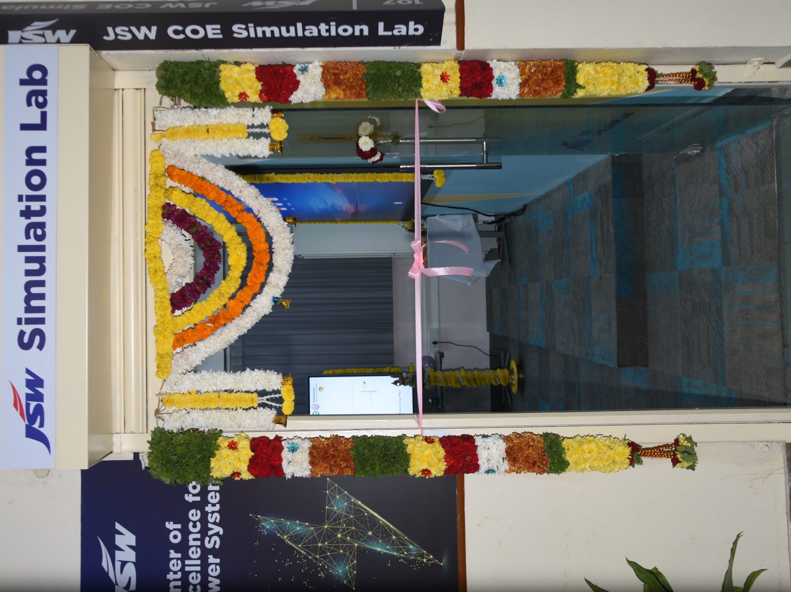
The JSW-CoE has been jointly established by JSW Group, Sharika Enterprises and MSRIT to address one of the most pressing challenges in the power sector today-maintaining grid stability amid the rapid growth of renewable energy.
India has made remarkable progress in adding solar, wind and Battery Storage Systems (BeSS). However, renewable energy brings variability and uncertainty that traditional grid systems were not originally designed to handle. This has created a gap between renewable energy generation, grid stability and market participation. The JSW-CoE has been set up with a clear purpose to bridge this gap through advanced system modelling, automation, analytics and real-time simulation.
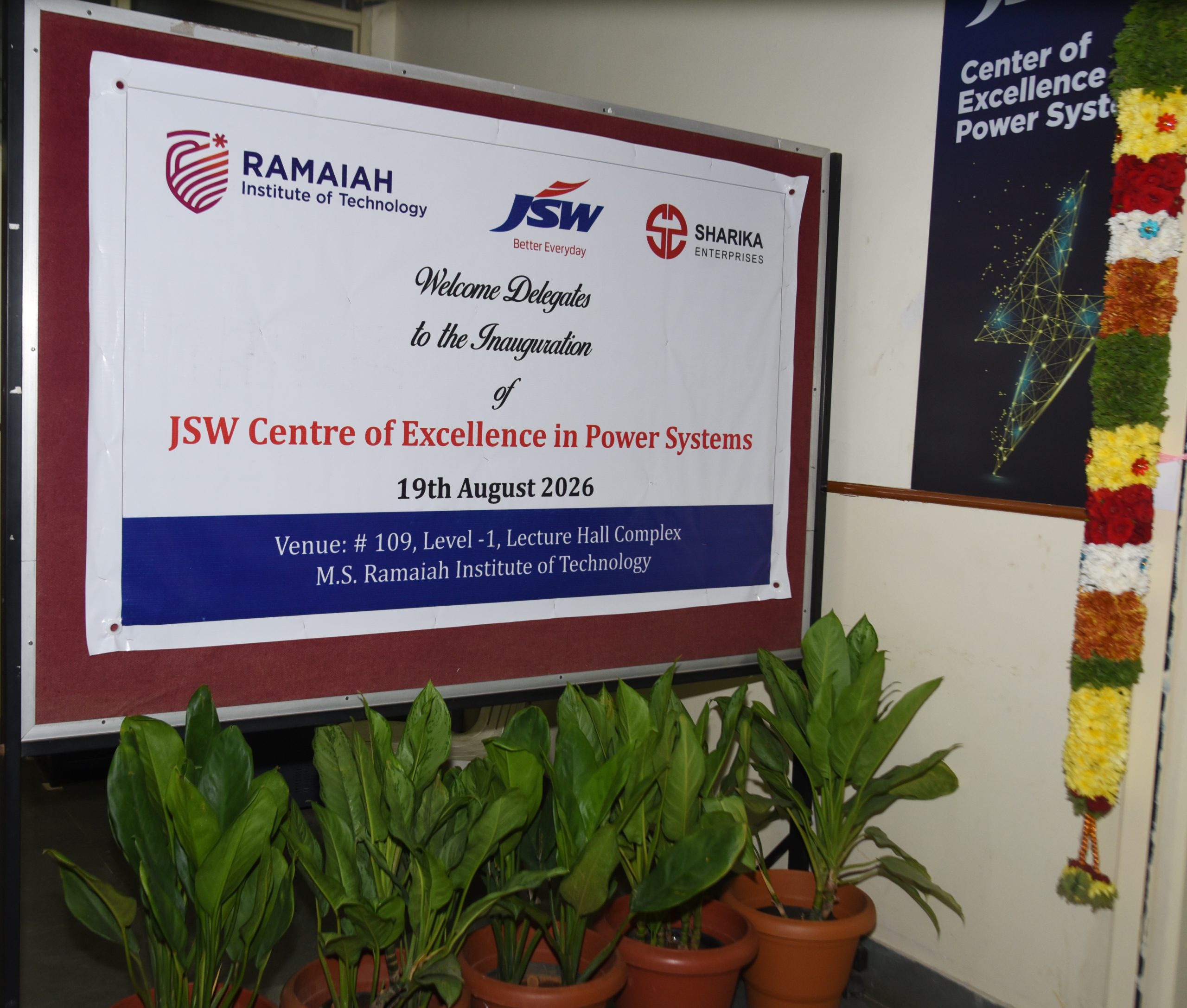
As per National smart grid mission under RDSS GOI has to establish several Centre of excellence in flexible power system across country to enhance capabilities in advanced power management practices to enhance operational efficiency and sustainability across our RE aggregation ecosystems. This Centre of Excellence in Power Systems reflects the commitment to strengthening the national grid infrastructure at a critical time. As renewable energy capacity grows, grid systems must become smarter, more stable and more market-ready. This initiative aims to support innovation, industry collaboration and the development of skilled professionals who can manage the complex power systems of the future.
The JSW-CoE operates on a unique Lab-as-a-Service model. JSW Group has funded the capital investment required to establish the advanced laboratory infrastructure. Sharika Enterprises has designed, set up and will manage the operations of the lab, drawing on its deep expertise in power automation, protection systems, Supervisory Control and Data Acquisition (SCADA) and international communication protocols such as IEC 61850 and IEC 60870. MSRIT hosts the JSW-CoE and provides the academic ecosystem to support research, certification and long-term skill development. The JSW-CoE has been structured as a non-profit entity, with a clear focus on capability building rather than commercial returns.
Mr. Rajinder Kaul, Chairman and Managing Director, Sharika Enterprises, said, “The power sector is undergoing a structural transformation. Utilities, renewable developers and system operators need access to real-world testing environments before deploying solutions in the field. This Centre has a capability to simulate a complete power system within a controlled lab environment, enabling stakeholders to simulate grid conditions, test automation solutions and prepare for market participation. Our goal is to build both technology readiness and human capability for the smart grids of tomorrow.”
The facility is designed to replicate generation, transmission and distribution systems in an integrated setup. It includes SCADA and dispatcher systems, renewable energy management platforms, PMU-based protection and wide-area monitoring and tools for real-time load flow studies, contingency analysis and energy market simulations. Industry players, startups, utilities and researchers can access the lab at a reasonable cost to test systems, validate solutions and prepare for deployment.
Convergence of academia and industry:
Beyond technology development, the Centre will focus strongly on skill building. Engineers of the future must understand power systems, communication protocols, real-time data management, automation, artificial intelligence and energy trading mechanisms. Through masters, certification courses and industry-linked projects, the JSW-CoE aims to create a pipeline of professionals equipped for India’s evolving power landscape.
Lauding the JSW-CoE, Dr. N V R Naidu, Principal, MS Ramaiah Institute of Technology, said, “The launch of the JSW-CoE at MSRIT represents a powerful convergence of academia and industry. As the power sector evolves with renewable integration and digital technologies, it is essential that our students and researchers gain hands-on exposure to real-world grid systems, automation platforms and advanced simulation environments. This collaboration will enable MSRIT to nurture the next generation of engineers who can contribute meaningfully to India’s smart grid and energy transition journey.”
The launch of the JSW-CoE positions Bengaluru as a growing hub for smart grid innovation and advanced power system research. By bringing together industry investment, academic strength and technical expertise, the initiative seeks to support India’s long-term power transition and ensure that renewable growth is matched by grid intelligence and market readiness.
The post JSW Centre of Excellence in Smart Grid and Automation Launched at MSRIT appeared first on ELE Times.
Ground broken on Alcoa-Sojitz Gallium Recovery Project in Western Australia
The Steam Deck has 3 PCBs per trackpad
 | submitted by /u/K0eg [link] [comments] |
Quintessent raises $40m in oversubscribed Series A funding round
Mouser website now blocks Linux users
 | Really baffling decision, my last order from them was only a few months ago. Apparently Linux is no longer a "standard" operating system! [link] [comments] |
🎥 У КПІ ім. Ігоря Сікорського урочисто відзначили День Державного Прапора України та День Незалежності України

🇺🇦 Сьогодні спільнота КПІ зібралася на площі Знань під синьо-жовтим прапором — одним із головних символів української державності.
TP-Link’s Tapo P125: A smart plug with an Apple HomeKit vibe

Does the addition of Apple smart home protocol support necessitate hardware augmentation and upgrade, or do firmware-delivered feature updates suffice?
After pausing my TP-Link smart plug teardown publication cadence in May, I temporarily paused again in July (although the company’s products weren’t completely overlooked last month, mind you). It’s August, and I’m back on the treadmill, this time with a look at the Tapo P125, which adds Apple HomeKit support to the Tapo P105 foundation I dissected at the beginning of June.

I’d bought a Tapo P125 two-pack from Amazon’s Resale website area last November during a 30%-off holiday promo sale, for $12.59. Here’s a stock shot of the Tapo P105 four-pack acquired at the same time, for comparison’s sake.

The two products are dimensionally identical (2.4 × 1.5 × 1.3 in, 60 × 38 × 33 mm) and more broadly visually similar, save for the Tapo P105’s front panel status LED, whose illumination-related information has been relocated to the side-located switch on the Tapo P125 (non-illuminated in the Tapo P105 predecessor).
A history revisitAs a reminder, as it’s been a while since I started this particular teardown-coverage sequence, my basic aspiration with this project is to ascertain to what degree (if any) differences in the company’s various smart plug products’ feature sets, broadly between the Kasa and Tapo product lines as well as between products within a given line, are due to hardware variability versus (or in addition to) software-implemented inconsistency.
Here’s the so-far published dissection list:
- TP-Link’s Kasa HS103: A smart plug with solid network connectivity
- TP-Link’s Kasa EP10: If at first it doesn’t connect, buy, buy again
- TP-Link’s Kasa EP25: Energy monitoring for a hoped-for utility bill nose-dive
- TP-Link’s Tapo P105: A Kasa EP10 clone, or evolutionarily derived?
Note that hardware changes can, of course, be developer-motivated not only by evolving feature set requirements but also by the phaseout and replacement of building block components inside these devices. Such supply chain impermanence also helps explain the multiple to-date hardware versions of each product as documented on TP-Link’s support site.
In the Kasa past, I made a two-notable-feature teardown jump from the EP10 to the EP25: not only added energy monitoring capabilities but also support for Apple HomeKit (and Siri, for that matter). In the more recent and ongoing Tapo era, the product feature iterations are more modest. As already noted, today’s Tapo P125 augments the baseline Tapo P105 with Apple HomeKit cognizance, while the Tapo P115 (dissection to come next month) instead adds energy monitoring capabilities.
And I’ll close out, hopefully before year end, with a teardown of the Tapo P110M: slightly wider albeit no taller (or shorter) or deeper (or shallower) than the Tapo 115 and also with energy monitoring support, but additionally offering Matter smart home ecosystem cognizance.
Enough of the background; let’s get to Tapo P125 tearing down. I’ll start with the remainder of the Amazon-hosted stock images, which for some unknown reason tend to be higher-resolution and otherwise higher quality than those on TP-Link’s own company and Tapo product sites.


This last one, always a pre-dissection favorite and in this case solely published on TP-Link’s own site, is the “conceptual teardown”.

Assuming it’s correct, it suggests a relocation of the mini-PCB containing digital circuitry from the upper corner of the device (seen below with the Tapo P105) back to the more common side locale.

As well as the re-integration of the LED onto that mini-PCB versus standalone and soldered to the main board in the Tapo P105 situation.

Let’s definitively confirm-or-deny the conceptual tease. Here are some box shots to start, as usual accompanied by a 0.75′′ (19.1 mm) diameter U.S. penny for size comparison purposes.


Per the obscured-but-still-faintly-visible box-bottom marking, the devices inside are based on v1.26 hardware (the initial release, per TP-Link’s support page, along with v1.6 and v1.8 successor versions). And what’s obscuring it is the as-usual additional sticker suggestive of, per its formerly-Warehouse origins, an initial customer return followed by an Amazon resale to me.

Often, albeit not always, such products were opened by their previous owners prior to being sent back (for various reasons, including malicious ones) for refund. So too was seemingly the case here, although the top of the box was still sealed (albeit damaged). When I instead initially opened it from the bottom, the cardboard around the then-left (normally right when upright) device’s plug was comparatively sullied versus that of its packaged companion.

Turning the box back over, cutting the clear plastic seal, and opening it revealed more evidence of the right-side device’s prior-owner disturbance.

So, I went with that one for the dissection.


Cute, huh?

Here’s our patient.


The bottom side perspective was as-usual the most informative from FCC ID (2AXJ4P125) and other info perspectives.


Time to dive inside, starting with the previously seen backside screw.


I’ve now done a few of these similar-form-factor dissections, and they seemingly get easier (for my body, if for no other reason) each time, since the first time.

This one was no exception to the trend…and yes, I realize I’ve just jinxed myself for future project(s) by typing those words.


Here comes the series of shots I know you’re all most interested in.


That blue-colored (this time) relay on the right, a common component (for…y’know…power switching reasons…) in all smart plugs I’ve taken apart to date as well as presumably also in the future, is this time a Churod A16-V-105DA2F, which we also found inside the Tapo P105.
Now for the smarts-packed mini-PCB on the left side.

Remove the foam square, zoom in, and:

That’s (once again) Realtek’s RTL8720, also previously found inside the Tapo P105, as well as in the Kasa EP25. Which might lead you to decide that although the mini-PCB and LED have been relocated (note the switch in the lower left corner this time, with the LED just to its right), the digital hardware is exactly the same as the Tapo P105. And which in fact seems to be a reasonable deduction, it turns out, although I’d initially thought otherwise.
The nexus of my initial confusion (putting aside my ever-present confusion about most if not all things) are the ICs you can’t see (clearly, at least) in my shots, on the mini-PCB backside, which was previously bare in the Tapo P105 case. Head back over to the FCC site, click on the Internal photograph link, and you’ll be able to see them for yourself.
The larger eight-lead chip, for example, is the exact same Eon Silicon Solution EN25Q32B 32 Mbit serial flash memory (marked QH32b-104HIP) as before. And the other, smaller, five-lead (two on one side, three on the other) SOT-packaged IC, marked FE1RYE and not noted (albeit still there) before, is function-unknown to me. On the Tapo P105, it (assuming my commonality assumption is correct) was marked ACeN2. Ideas, readers?
In closing, I as usual was unable to gain access to the PCB backside, although as you might be able to discern from these shots, there’s not much there to write home about, anyway.


If you really care, the FCC site is always there to alternatively satiate your solder-blob appetites. With that, I’ll wrap up for today. Reader thoughts are as-always welcome in the comments!
—Brian Dipert is the associate editor, as well as a contributing editor, at EDN.
Related Content
- TP-Link’s Tapo P105: A Kasa EP10 clone, or evolutionarily derived?
- Tapo or Kasa: Which TP-Link ecosystem best suits ya?
- TP-Link’s Kasa EP10: If at first it doesn’t connect, buy, buy again
- TP-Link’s Kasa HS103: A smart plug with solid network connectivity
- TP-Link’s Kasa EP25: Energy monitoring for a hoped-for utility bill nose-dive
The post TP-Link’s Tapo P125: A smart plug with an Apple HomeKit vibe appeared first on EDN.
US Rapid-Tracks ‘Containerised Laser’ Weapons for Drones and Missiles
The United States finalized two Joint High Energy Laser Weapon System contracts with nLIGHT Defence and Lockheed Martin Aculight on 9 th July 2026. This programme’s first contract awards are worth around $86 million, and its potential value is $847 million. With the help of this experimental display to be production-ready to oppose drone technologies along with travelling defence systems. High-energy lasers should be operating at the power range between 150 kilowatts for current designs and between 300 and 500 kilowatts required for advanced cruising defence engagement targets. Another incorporated system to operate at 500 kilowatts would be designed with the aid of tech established by the High Energy Laser Scaling Initiative.
Unlike interceptors, laser-powered weapons fire with no projectiles, travelling at the speed of light, and don’t need to launch missiles with every shot. So long as you have electricity for power, and a way to cool it down, a laser can have almost an effectively infinite capacity, and relatively low per-shot costs, perfect for swarms of large drones. The laser weapons will be relatively large and come in a modular, containerised format for placement on top of ground-based vehicles and for warships. The major hurdles to overcome include the effects of intervening air on the beam, focusing the weapons, getting it to cool down effectively, and consistently generating enough electricity.
The post US Rapid-Tracks ‘Containerised Laser’ Weapons for Drones and Missiles appeared first on ELE Times.
Indigenous Sonars Reinforce New Naval Warships
India has deployed indigenous sonars on board two newly inducted warships- the guided-missile stealth frigate INS Dunagiri and the anti-submarine warfare shallow water craft INS Agray- which were commissioned in Kolkata on 21 st June 2026, carrying more than 75% indigenous equipment. The sonar systems have been designed by the Naval Physical and Oceanographic Laboratory, Kochi, of DRDO, and are manufactured by Bharat Electronics. INS Dunagiri is fitted with the HUMSA system known as HUMSA-2020, which is otherwise known as HUMSA-NG Mk II, employing contemporary electronics architecture for the purpose of long-range underwater detection and target acquisition capability. It has already undergone laboratory, factory, and ship-acceptance tests, and the sonar systems have been successfully accepted for deployment on board Indian Naval platforms.
INS Agray is equipped with Abhay PG shallow-water sonar suite. It is a light, hull-mounted suite that is meant for service in the littoral zones, where underwater terrain variations, reefs, shallow waves reflection and civilian ships produce lots of underwater acoustic clutter and acoustic interference. The sonar suite will be installed on 16 shallow water boats. It is to act as the underwater ‘ears and eyes of vessels’ to help track, classify and hunt submarines and other underwater threats, thereby aiding its anti-submarine warfare (ASW) capabilities, while minimizing India’s dependence on foreign sensors.
The post Indigenous Sonars Reinforce New Naval Warships appeared first on ELE Times.
TigerShark Set to Implement F1 Engineering Techniques on Extended-Range Missions.
The British company MGI Engineering is developing TigerShark- an autonomous, long-range offensive drone seen as a cheaper solution than cruise missiles. TigerShark is inspired by innovations from Formula One racing and other advanced engineering sectors, allowing it to serve as a quickly assembled, highly modular unmanned aircraft. Apparently, TigerShark is 5.5 meters in length, with a wingspan of 4.3 metres, and powered by two small turbojet engines. The aircraft is launched by a rocket booster from a mobile ground installation, can reach a speed of 750 kilometres per hour, can be equipped with up to 300 kilograms of modular loads, and can fly to a distance of about a thousand or more kilometres.
Aircraft include Auterion Skynode flight computer along with software. Inertial navigation and terrain-following are conceived to aid operation in areas of GPS-denied or interference. The weapon’s modular payloads bay is said to be large enough for traditional, EW or specialized warheads. Groups of TigerShark would be considered for an attack in an attempt to overwhelm and force an enemy air defence net and/or to prosecute a specific high-value target. These announced capabilities and production plans are expected to undergo additional development and client evaluation. This program is similar to the growing trend of developing rapidly produced, cheap, and software-denied deep strike weapon systems.
The post TigerShark Set to Implement F1 Engineering Techniques on Extended-Range Missions. appeared first on ELE Times.
Japan Set to Demonstrate Helsing’s AI-Based HX-2 Strike Drone
Japan’s Ground Self-Defence Force will field test the HX-2 strike drone from Helsing, and the trials will run till the end of the Sept 2026. Rakuten is helping the German defence technology company navigate Japan’s procurement environment to secure a possible supply contract. The HX-2 is a software-defined all-electric loitering munition which could be used to attack artillery, armor, and fixed military targets, has a maximum range of 100 km and a weight of around 12kg; the drone could be configured with multipurpose, anti-tank and anti-structure warheads.
However, its cutting-edge technology is the on-board artificial intelligence; Helsing maintains the drone’s search-reacquisition capability without a persistent data link, allowing it to operate under a jammed satellite navigational and communication system, but critical engagement decisions still rest with man. In addition, HX-2 will integrate with Altra software, which is a reconnaissance-strike system, enabling remotely piloted aircraft (RPVs), reconnaissance, and cooperation with one another. OTA software updates enable the software to meet evolving threats. Thus, it is concluded that Japanese trials reflect the increasing need for a mass-produced UAV in a high electronic warfare domain.
The post Japan Set to Demonstrate Helsing’s AI-Based HX-2 Strike Drone appeared first on ELE Times.
Сторінки




![[link]](https://i.redd.it/aq9khnvndklh1.png)
![[link]](https://i.redd.it/3zdj7yhz7clh1.jpeg)