
Збирач потоків
Graphene in Focus: How Nanotechnology is Transforming Electronics?
As miniaturisation and increasingly complex design architectures continue to define modern technology, nanotechnology is emerging as a frontier discipline shaping the trajectory of innovation—from medical and electronic devices to energy infrastructure and beyond. Simply stated, as the focus of electronics development shifts towards the engineering and application of materials at the atomic and molecular scale—typically between 1 and 100 nanometres—certain physical, chemical, and electrical limitations begin to surface. When conventional materials such as silicon and copper are miniaturised to the nanoscale, they often encounter issues such as increased resistance, heat generation, and reduced performance. To address these limitations, Graphene, an sp²-hybridized two-dimensional honeycomb lattice, has emerged as one of the most promising materials for next-generation electronic systems.
Amid rapid advances across the nanotechnology landscape, graphene is increasingly regarded as a flagship material in nanoscale engineering, attracting significant attention, particularly in electronics.
While Graphene continues to attract significant research interest due to its exceptional properties, the transition from laboratory-scale breakthroughs to commercially viable semiconductor technologies remains a complex challenge. Industry players such as Weebit Nano emphasise that beyond material performance, factors such as manufacturability, process compatibility, and scalability are equally critical. This creates a dynamic balance in nanoelectronics—between exploring high-potential emerging materials and developing solutions that can be seamlessly integrated into existing semiconductor fabrication ecosystems.
Owing to its exceptional electrical conductivity and extremely high electron mobility, graphene is being explored for a wide range of electronic components, including high-speed transistors, flexible circuits, and highly sensitive biosensors. The material is both electrically and thermally efficient, enabling electronic devices to operate with improved performance while generating less heat. These properties have positioned graphene as a promising complement—and in some cases a potential alternative—to conventional materials such as silicon in applications including touchscreens, sensors, and next-generation electronic interfaces.
When nanotechnology converges with electronics, the field is commonly referred to as Nanoelectronics. Nanoelectronic systems require extremely high switching speeds and efficient charge transport while minimizing heat buildup in densely packed circuits. In this context, Graphene offers exceptional carrier mobility—reaching approximately 100,000 cm²/V·s under ideal conditions—making it an attractive material for high-frequency electronic applications. Additionally, as electronic components become increasingly dense in nanoelectronic architectures, thermal management becomes a critical challenge. Graphene’s remarkably high thermal conductivity enables efficient heat dissipation, thereby helping maintain the reliability and performance of nanoscale electronic systems.
Let’s look into some applications of Graphene in nanoelectronics:
Graphene Field-Effect Transistors (GFETs)
Graphene Field Effect Transistors are advanced, ultra-sensitive electronic components comprising a channel made of a single-atom-thick layer of graphene, enabling modulation of current by an electric field.
Structure: A GFET typically consists of three things: Source, drain & a gate (top or back).
- Channel: The space between the Source & the Drain makes up a channel where a 2D Sheet of Graphene is placed.
- Gate Control: The gate voltage modifies the electric field, changing the charge carrier density in the graphene channel.
How does it work?
It operates by controlling the flow of electrical current through the Graphene channel. When a voltage is applied between the source and drain, charge carriers in the graphene layer begin to move, creating a current. The gate electrode, separated from the graphene by an insulating dielectric layer, is used to control this current. By applying a positive or negative voltage to the gate, an electric field is generated that changes the concentration of electrons or holes in the graphene channel.
A positive gate voltage increases electron concentration, while a negative gate voltage increases hole concentration, thereby modulating the conductivity of the channel and controlling the amount of current that flows between the source and drain. Because graphene has extremely high carrier mobility, electrons can move through the channel very quickly, allowing GFETs to operate at very high frequencies, which makes them particularly promising for radio-frequency and high-speed electronic applications.
Applications
GFETs are used in various fields due to their high performance:
- Biosensors & Chemical Sensors: For detecting DNA, proteins, and gases at low concentrations.
- Flexible Electronics: For wearable sensors and devices.
- Radio Frequency (RF) Electronics: Due to high-speed charge transport.
Nano-Electro- Mechanical Systems (NEMS)
Nano-Electro -Mechanical Systems are highly miniaturized devices that integrate electrical and mechanical functionality at the nanoscale, enabling the development of devices that are smaller, more sensitive, and more efficient as compared to the traditional silicon-based ones.
Structure: The structure of a Graphene-based Nanoelectromechanical System (graphene NEMS) generally consists of a few key components integrated on a microfabricated substrate. It Includes:
- Silicon Base: At the base is a Silicon or silicon-oxide substrate in which a small cavity or trench is created.
- Electrodes: Metal source and drain electrodes are patterned on the surface to provide electrical contacts. A thin insulating layer may also be included to isolate different parts of the device.
- Graphene Sheet: The central element is a suspended sheet of Graphene, which spans the cavity and connects the electrodes, forming a bridge-like membrane.
- Gate Electrode: In some designs, a gate electrode is positioned beneath the graphene, separated by a dielectric layer.
How does it work?
A Nanoelectromechanical System (NEMS) functions by converting mechanical motion at the nanoscale into electrical signals, or vice versa. These devices integrate mechanical structures—such as beams, membranes, or resonators—with electronic components on a very small scale.
When voltage is applied between electrodes (such as source, drain, or gate), electrostatic forces drive the mechanical motion of the nanoscale structure, and with this, the mechanical component begins to deflect, vibrate, or resonate. This mechanical movement changes certain electrical properties of the system—such as resistance, capacitance, or current flow—which can then be detected and measured by the electronic circuitry. As a result, NEMS devices operate as ultra-sensitive sensors, resonators, or switches, capable of detecting extremely small physical changes at the nanoscale.
Applications:
NEMS are used in various applications, including:
- Ultra-Sensitive Sensors: NEMS devices, such as AFM tips, detect forces, vibrations, and chemical signals at the atomic level. They are used as highly sensitive accelerometers for inertial navigation and motion detection.
- Bio-nanotechnology & Medical: NEMS enables lab-on-a-chip devices for diagnostics, biomolecule detection, and precise, targeted drug delivery systems.
- Nano-switches and Relays: NEMS switches serve as mechanical, low-power alternatives to traditional semiconductor logic switches, offering near-zero leakage current.
Conclusion
As the electronics industry continues to push the boundaries of miniaturisation and performance, materials engineered at the nanoscale will play an increasingly central role in shaping the next phase of technological evolution. Among these, Graphene stands out for its exceptional electrical, thermal, and mechanical properties, offering solutions to several limitations faced by conventional semiconductor materials.
However, the path from material innovation to large-scale deployment remains complex. While graphene continues to demonstrate immense potential in nanoelectronic applications—from high-frequency transistors to ultra-sensitive nanoscale systems—its integration into mainstream semiconductor manufacturing is still an evolving challenge. In contrast, industry players such as Weebit Nano are focusing on developing technologies that align closely with existing fabrication ecosystems, underscoring the importance of manufacturability alongside performance.
As nanotechnology matures, the future of electronics will likely be shaped by a careful balance between breakthrough materials and practical implementation—where innovation is not only defined by what is possible at the nanoscale, but also by what can be reliably produced at scale.
The post Graphene in Focus: How Nanotechnology is Transforming Electronics? appeared first on ELE Times.
The 6G clock ticking: Why silicon architecture for 2030 must start in 2026

The 6G transition is no longer a distant theoretical exercise; it’s a commercial inevitability driven by fundamental requirements for cellular standards to keep moving forward. 5G penetration has already surpassed 75% and is on a trajectory to reach 95% within a few years. We are witnessing an appreciation for continued call quality and data throughput improvements despite an explosion in mobile traffic.
However, the wireless ecosystem projects that even this capacity will soon overload due to accelerating AI content, the integration of satellite communications (SATCOM) into the cellular fold, and the rise of physical AI. 6G is the industry’s response to keep pace with that exponential growth in data communication demand.
The 2030 countdown: Why 2026 is the crucial starting line
To understand the urgency, one must look at the decadal cycle of cellular evolution. History shows it takes about five years to finalize a standard and fold its requirements into a functional ecosystem. While 6G is anticipated to take off commercially by 2030, the work-back schedule reveals a tight timeline for product builders. By 2029, hardware must be ready for compliance testing, meaning component technologies must be finalized by 2028.
Consequently, underlying embedded systems must be built in 2027, necessitating that architectural definitions start as early as 2026. As an example of what is going on in the industry, Qualcomm’s CEO recently hinted at the Snapdragon Summit that 6G-capable devices could appear as early as 2028 for trials, making the 2028 Olympics a perfect arena for tech demos.
Unlocking the “Golden Band”: FR3 and the business of spectrum
Beyond architectural shifts, 6G introduces the Frequency Range 3 (FR3) spectrum, spanning 7.125 GHz to 24.25 GHz. Often called the “Golden Band for 6G,” FR3 offers the perfect balance between the wide coverage of lower bands and the massive capacity of mmWave.
This spectrum is expected to be a major business driver, enabling the 10x higher data rates targets (up to 200 Gbps) and supporting “massive MIMO evolution” to handle the projected 4x traffic growth by 2030 (going over 5.4 zettabytes as indicated by the GSMA Intelligence report).
Sustainable networks
Sustainability is a core pillar of 6G, with network operators seeking to reduce OpEx, as 25% of it is driven by power demand. 6G moves from an “always-on” to a “smart-on” philosophy, aiming for 30-50% increase in power efficiency. Key techniques include:
- Enhanced deep sleep modes: Enabling base stations to achieve near-zero power consumption when no active users are present, and reduction in periodic signaling (current 5G standard mandates high periodic signaling that in practice keeps a lot of the RF and power amplifier components active at all times).
- AI-driven beamforming: Using AI to direct signals precisely to users, reducing energy waste from broad, inefficient broadcasting.
- AI-driven resource management: Using AI at the higher protocol layers for effective radio resources management.
The AI-native revolution: Moving intelligence to the air interface
One of the most significant shifts in 6G is the move toward an AI-native air interface. Unlike 5G’s rigid mathematical models, 6G uses deep learning to dynamically adapt signal processing blocks. This enables “adaptive waveforms” that adjust modulation in real-time to environmental conditions.
It also facilitates integrated sensing and communication (ISAC), where RF reflections provide precise spatial awareness, allowing the network to proactively adjust beamforming based on user movement.
The coordination challenge: Managing two-sided AI
This transition introduces a complex challenge in how the transmitter (base station) and receiver (device) coordinate their intelligence. Unlike traditional algorithms, AI components must be synchronized through AI lifecycle management (LCM). The industry is weighing one-sided models (device-only optimization) against two-sided architectures (essential for tasks like CSI compression).
In two-sided designs, the device acts as a neural encoder and the base station as a decoder; these must be coordinated pairs to some extent. The level of coordination is still in study, as there are few optional schemes. Examples for those schemes are fully matched neural networks couples, or alternatively, independent at the NN architecture level but trained on the same dataset.
This raises critical questions on the protocol level: should the network use model ID-based selection (activating pre-loaded models) or model transfer (pushing new neural weights over the air) or weights transfer?
Programmable intelligence: Why DSPs are the preferred path
Because 3GPP specifications remain fluid, the need for flexibility through programmability has never been higher. Developing 6G on hard-wired logic is risky, as spec changes could render silicon obsolete. This is why digital signal processors (DSPs) are the preferred architecture. Modern DSPs are uniquely suited for the AI-native physical layer; they possess the massive number of MACs required for matrix operations and are highly efficient at the vector processing necessary for neural networks.
Leading technology vendors also offer dedicated AI ISA for accelerated NN activation functions. A fully programmable modem powered by AI-native DSP offers a “safe bet,” allowing developers to adapt as 6G settles while maintaining the performance needed to lead the market.
Elad Baram is director of product marketing for the Mobile Broadband Business Unit at Ceva.
Related Content
- Get ready for 6G
- 5G & 6G: Adoption, technologies and use cases
- 5G-Advanced to 6G: What’s next for wireless networks
- Making waves: Engineering a spectrum revolution for 6G
- The aspects of 6G that will matter to wireless design engineers
The post The 6G clock ticking: Why silicon architecture for 2030 must start in 2026 appeared first on EDN.
FormFactor and Rohde & Schwarz Advance their Partnership for on-wafer RF Component Characterisation
FormFactor and Rohde & Schwarz have announced a strategic co-marketing partnership as part of FormFactor’s MeasureOne partner program, a solution-integration initiative designed to deliver validated, turnkey on-wafer test systems. The collaboration combines advanced probing technology from FormFactor with industry-leading RF test instrumentation from Rohde & Schwarz, providing manufacturers with comprehensive solutions spanning early design verification through production. With RF device complexity and operating frequencies continuing to increase, this expanded collaboration formalises a tightly integrated on‑wafer test solution designed to lower integration effort and risk, reduce overall cost, and accelerate time-to-market for customers across development and production.
Reduced costs and faster time-to-market
On-wafer device characterisation of RF components such as 5G frontends or filters enables design validation during development, as well as product qualification and verification in production. Identifying faulty devices before packaging can significantly help reduce costs and improve yield. Through their integrated solutions, Rohde & Schwarz and FormFactor help manufacturers detect issues early in the process, which can result in faster time-to-market.
Seamlessly integrated test solutions
Rohde & Schwarz and FormFactor have been working together for several years to deliver powerful, seamlessly integrated solutions. Rohde & Schwarz provides instruments like the R&S ZNA, a versatile high-end VNA capable of measuring all key RF parameters, which can easily be combined with frequency converters extending frequencies up to the THz range. FormFactor complements this with a comprehensive portfolio of manual, semi-automated, and fully automated probe systems, including advanced thermal control, high-frequency probes, precision probe positioners, and robust calibration tools.
This combined approach allows manufacturers to validate product performance directly during wafer runs, leveraging the expertise of both companies. The tight integration of hardware and software components from both companies is designed to enable fast and reliable testing. The complete solution includes advanced instruments, reliable wafer and die fixuring, and high-precision probe positioning throughout the entire test cycle, strengthening confidence in product quality and performance.
Jens Klattenhoff, SVP and GM of the Systems Business Unit at FormFactor, said: “By expanding our collaboration with Rohde & Schwarz through the MeasureOne program, we are delivering integrated on‑wafer RF test solutions designed to help customers reduce risk, improve efficiency, and accelerate development. This partnership brings together advanced wafer probing and proven RF measurement technologies to address the growing complexity of next‑generation semiconductor devices.”
Michael Fischlein, Vice President, Spectrum & Network Analysers, EMC and Antenna Test at Rohde & Schwarz, stated: “We are delighted to be part of MeasureOne, a strategic Co-Marketing partner program that unites FormFactor – one of the world’s leading probe station providers – with Rohde & Schwarz, a global leader in test and measurement. Together, we are set up to deliver turnkey on-wafer solutions enabling crucial and demanding test capabilities for next-generation semiconductors.”
The MeasureOne partnership encompasses a wide range of Rohde & Schwarz instruments, including the R&S ZNA, R&S ZNB, R&S ZNBT, R&S ZVA and R&S ZNL VNA families, alongside signal and spectrum analysers such as the FSW, FSWX, R&S FSV3000 and R&S FSVA3000. Integration also extends to signal generators (R&S SMA100B, R&S SMB100B, R&S SGS100A, R&S SGU100A) and selected frontends and converters for advanced calibration workflows, all working seamlessly with FormFactor’s traditional plus speciality probe stations for cryogenic and vacuum applications.
The post FormFactor and Rohde & Schwarz Advance their Partnership for on-wafer RF Component Characterisation appeared first on ELE Times.
Anritsu and SK Telecom Jointly Verify AI-Based Antenna Optimisation, POSTECH and Bluetest
ANRITSU CORPORATION has jointly verified AI-based antenna optimisation technologies with SK Telecom, South Korea’s leading mobile network operator, Pohang University of Science and Technology (POSTECH), and Bluetest of Sweden.
In this verification, MIMO measurement data were acquired in a real user environment using Anritsu’s Radio Communication Test Station MT8000A and Universal Wireless Test Set MT8870A. Based on AI-based analysis and optimisation technologies, the effectiveness of antenna performance optimisation was confirmed.
Details of this joint verification were also presented at MWC Barcelona 2026 (MWC 2026), one of the world’s largest mobile communications exhibitions.
This verification analysed antenna performance based on throughput and ECC (Error Correlation Coefficient) data collected from real user environments. It reflected practical usage conditions, including free-space scenarios, handheld operation, and head-proximate usage scenarios. By incorporating a variety of user grip conditions, it quantitatively evaluated performance variations under time-varying RF conditions.
Through AI-based analysis, RF performance differences according to antenna tuner states were modelled, and the optimal antenna switching configuration was automatically identified. This enabled dynamic optimisation of antenna performance while maintaining communication quality in real user environments.
Based on measurement-driven evaluation results, significant throughput improvements were confirmed across various user scenarios in an 8Rx (eight-receive-antenna) configuration, while in a 4Tx (four-transmit-antenna) configuration, throughput improvement of up to more than two times was observed.
Verification Overview
This verification presented an AI-based antenna optimisation workflow built on real measurement data collected in an Over-the-Air (OTA) test environment.
The verification covered the following processes:
- Analysis of RF performance variations according to user scenarios and tuner state changes
- Comparison of power and performance characteristics for each antenna path
- Derivation of optimal switching states based on throughput and ECC data
- Verification of performance improvement through AI analysis based on measurement data
This approach goes beyond conventional static antenna design-centric evaluation, enabling data-driven optimisation verification that reflects real environmental conditions.
MT8000A (5G NR Test Platform)
MT8000A is an integrated RF and protocol-based test platform for 5G NR device validation. In this verification, it was used for MIMO performance analysis and throughput evaluation in an OTA environment.
Key features include:
- 4×4 / 8×8 MIMO signal generation and OTA data acquisition
- Multi-port synchronised measurement based on digital IQ capture
- Throughput evaluation under controlled 5G NR link conditions
- Provision of a repeatable and stable RF test environment
MT8000A provided high-precision signal generation and analysis capabilities for measurement-based performance verification, supporting the acquisition of highly reliable data required for AI modelling.
MT8870A (RF Measurement Platform)
MT8870A is a general-purpose wireless measurement platform supporting non-signalling RF measurements. In this verification, it was used for RF characteristic analysis by antenna path and comparative measurement of switching states.
Key features include:
- RF power measurement by antenna path under various tuner states
- TX/RX path control and RF characteristic measurement
- Collection of measurement data across antenna paths and switching states
- Support for multi-port RF measurement configurations
The path-specific RF characteristic data obtained through MT8870A is used as core input data for AI-based optimisation analysis.
The post Anritsu and SK Telecom Jointly Verify AI-Based Antenna Optimisation, POSTECH and Bluetest appeared first on ELE Times.
Western Electric 704A Subminiature UHF Diode Radar Mixer/Detector
Just finished repairs on an ESI 252 LCR meter
 | Measuring an 8 picofarad capacitor. [link] [comments] |
Polar Light awarded €1.1m EU grant for 18-month 2ndGenMicroLED project
Taiwan Semiconductor introduces AEC-Q-qualified 1200V SiC Schottky rectifiers in SOD-128 packages
Guerrilla RF launches 6–8.5GHz GRF2118 X-band LNA
3D printing a solderpaist screen with a Ender3V2 printer.
 | Well, I made a post awhile back about 3D printing a solder paist mask. I was finally able to mod/tune my 3d printer enough to get something usable. I outfitted my Ender3 V2 printer with a 0.2mm nozzle and gave my layer height a setting of 0.1mm. Please note that this was never for production boards as I am only doing 2 or 3 prototype boards with it. There is one or two glitchy areas with it which i attribute to not having dry filliment. Doing this will definitly save a lot of time manually putting paist on the boards. [link] [comments] |
🎓 STEM-стипендія для студентів НН ІПСА від фінтех-компанії Solidgate

Національний технічний університет України «Київський політехнічний інститут імені Ігоря Сікорського» та Solidgate оголошують про запуск першої STEM-стипендії для студентів Навчально-наукового інституту прикладного системного аналізу.
🉐Відкрито набір на довгостроковий курс японської для початківців!
Курс складається з 64 занять. Увага приділяється всім аспектам мови: Ви вивчите 2 японських алфавіти, базовий набір ієрогліфів, основи граматики, а головне — звісно, основи комунікації японською мовою.
1MHz 555 VFC

For decades, I’ve had a fascination with voltage-to-frequency converters and the 555 analog timer chip, and therefore a double obsession with VFCs based on the 555. In fact, my first Design Ideas (DI) submission (in 1974) was for a 555 VFC. It was not only published but also selected as the best DI of the year. That was it, I was thenceforth hooked forever.
Wow the engineering world with your unique design: Design Ideas Submission Guide
The simple 555 VFC design to be presented here, so far as I know and as unlikely as it sounds for so *ahem* “mature” a part as the 555, is novel. It runs with good linearity and accuracy at 1 MHz, with even faster operation possible. That’s 100x faster than that 1974 555 frequency converter.
I hope you’ll find its details interesting. Here’s how it works. The story begins with Figure 1.

Figure 1 Starred components are precision, including the +5 V supply, but something’s missing.
There’s nothing novel about the input current source comprising A1, Q1, and surrounding parts. It supplies 0 to 1 mA to the U1 current-to-frequency converter in response to its input voltage, as scaled and offset by R1 and R2. The values shown set a 0 to +5 V input span. R1 = 1.8M and R2 = 200k would make it -5 V to +5 V.
A capacitor added in parallel with R2 will provide extra noise rejection. But the inherent noise immunity of the VFC analog-to-digital conversion is good, so you probably won’t need it.
Moving further into the circuit is when things do start to get weird, because the usual two resistors associated with 555 oscillators are missing. Also missing is the usual astable 555 1/3V+ peak-to-peak voltage swing. This topology generates a 2/3V+ Vpp linear sawtooth waveform that resets, not to V+/3, but to zero. Unfortunately, while the sawtooth is nicely linear, due to U1’s internal switching delays Td, the frequency versus Q1 current Iq1 relationship is not very linear. Figure 2 shows how bad it is:
Frequency of oscillation (FOO) = 1.0/((VthC2/Ir3 + Td) = 1.0/(1.0ns/Ir3 + Td)

Figure 2 Nonlinear red curve versus ideal black shows ~20% linearity error from LMC555 internal delays.
Luckily, as derived in another recent DI: “Improve 555 frequency linearity.“
…it’s an easy fix. It consists of a single resistor, R4, connected between the Dch (discharge) and Thr (threshold) pins. R4 is used to linearize the current-versus-frequency function by biasing the Thr pin upward by IcR4. That cuts short the duration of the positive-going timing ramp and thereby the sawtooth period by the same amount that the delays lengthen it: IcR4/(Ic/C2) = R4C2 = Td.
Thus, if R4 is chosen so R4C2 = Td as shown in Figure 3, nonlinearity compensation will be (at least theoretically) complete over the full range of control current. The frequency of oscillator (FOO) for this circuit:
FOO = 1/((VthC2)/Iq1 + 212ns – Td) = 1/(1.0ncb/Iq1 + 212ns – 212ns) = 1/(1.0ncb /Iq1) = 1000 Iq1 MHz = 1MHz(+5v – Vin)/+5v

Figure 3 R4C2 = Td = 212ns = nonlinearity compensation for 555 internal delays.
Now FOO will linearly track Iq1 and therefore Vin as shown in Figure 4.

Figure 4 Nonlinearity disappears if R4 = Td/C2 =212 ns/300 pF = 706 ohms.
Stephen Woodward‘s relationship with EDN’s DI column goes back quite a long way. Over 200 submissions have been accepted since his first contribution back in 1974. They have included the best Design Idea of the year in 1974 and 2001.
Related Content
- Improve 555 frequency linearity.
- Tune 555 frequency over 4 decades
- 555 VCO revisited
- Inverted MOSFET helps 555 oscillator ignore power supply and temp variations
- Gated 555 astable hits the ground running
The post 1MHz 555 VFC appeared first on EDN.
Gartner Predicts That by 2030, Performing Inference on an LLM With 1 Trillion Parameters Will Cost GenAI Providers Over 90% Less Than in 2025
By 2030, performing inference on a large language model (LLM) with one trillion parameters will cost GenAI providers over 90% less than it did in 2025, according to Gartner, Inc., a business and technology insights company.
AI tokens are the units of data that GenAI models process. For the purposes of this analysis, a token is 3.5 bytes of data, or approximately 4 characters.
“These cost improvements will be driven by a combination of semiconductor and infrastructure efficiency improvements, model design innovations, higher chip utilisation, increased use of inference-specialised silicon, and application of edge devices for specific use cases,” said Will Sommer, Sr. Director Analyst at Gartner.
As a result of these trends, Gartner forecasts that LLMs in 2030 will be up to 100 times more cost-efficient than the earliest models of similar size developed in 2022.
The forecasted model results are split between two sets of semiconductor scenarios:
- Frontier scenarios: Model processing is based on a representation of cutting-edge chips.
- Legacy blend scenarios: Model processing is based on a representative blend of available semiconductors benchmarked to Gartner forecasts.
Modelled costs in the “blend” forecast scenarios are considerably higher than in the “frontier” scenarios, given lower computational power (see Figure 1).
Figure 1: Gartner GenAI Inference Cost Scenario Forecasts
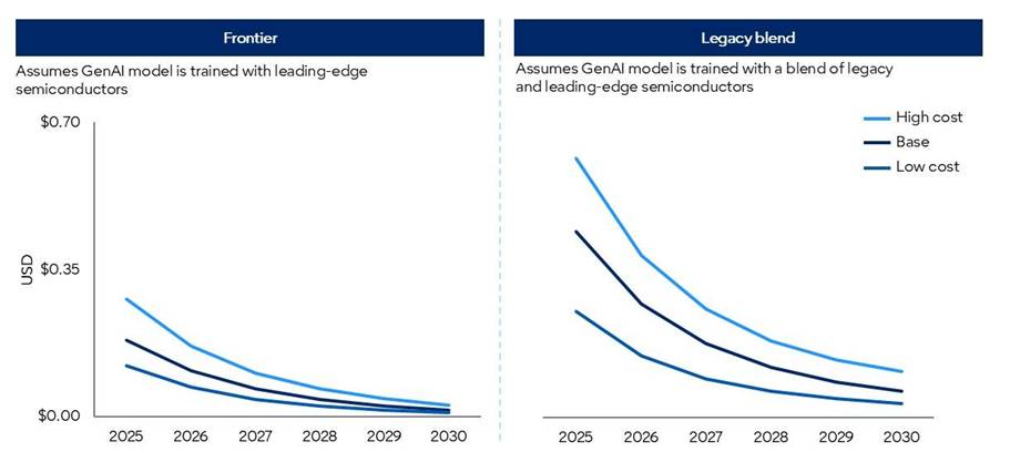
Source: Gartner (March 2026)
Falling Token Costs will not Democratize Frontier Intelligence
However, falling GenAI provider token costs will not be fully passed on to enterprise customers. Moreover, frontier intelligence will demand significantly more tokens than current mainstream applications. Agentic models, for example, require between 5-30 times more tokens per task than a standard GenAI chatbot, and can perform many more tasks than a human using GenAI.
While lower token unit costs will enable more advanced GenAI capabilities, these advancements will drive disproportionately higher token demand. As token consumption rises faster than token costs fall, overall inference costs are expected to increase.
“Chief Product Officers (CPOs) should not confuse the deflation of commodity tokens with the democratisation of frontier reasoning,” said Sommer. “As commoditised intelligence trends toward near-zero cost, the compute and systems needed to support advanced reasoning remain scarce. CPOs who mask architectural inefficiencies with cheap tokens today will find agentic scale elusive tomorrow.”
Value will accrue to platforms that can orchestrate workloads across a diverse portfolio of models. Routine, high-frequency tasks must be routed to more efficient small and domain-specific language models, which perform better than generic solutions at a fraction of the cost when aligned to specialised workflows. Expensive inference of frontier-level models must be heavily gated and reserved exclusively for high-margin, complex reasoning tasks.
The post Gartner Predicts That by 2030, Performing Inference on an LLM With 1 Trillion Parameters Will Cost GenAI Providers Over 90% Less Than in 2025 appeared first on ELE Times.
Infineon partners with Zenergize on power electronics for India’s energy transition
Київський політехнік Ігор Ментюков на Всесвітніх іграх майстрів

Київський політехнік Ігор Ментюков виступив у складі української футбольної команди ветеранів, яка виборола першість на Всесвітніх іграх майстрів. Нещодавно в місті Абу-Дабі (ОАЕ) відбулися Всесвітні ігри майстрів – ветеранів спорту.
Chiplets: 8 best practices for engineering multi-die designs

Semiconductor design is in the midst of a structural shift. For decades, performance gains were achieved by packing more transistors into single, monolithic dies. But the physical limitations of these dies—and the process technologies used to create them—are at odds with the ever-increasing compute, memory, and I/O demands of modern workloads. In other words, process technology advances alone are not enough to keep up with modern workloads.
Stepping in to address these demands are multi-die designs, which combine several smaller dies (known as chiplets) inside a single standard or advanced package. These multi-die architectures are reshaping how engineers build everything from AI accelerators to automotive ADAS systems. By disaggregating compute, memory, and I/O, teams can mix and match chiplets—often from different process nodes—to optimize performance, energy efficiency, size, or cost.
However, multi-die designs introduce new engineering complexities and design considerations, spanning packaging, verification, thermal dynamics, and more.
Here are eight best practices for developing chiplet designs.
- Leverage the ecosystem
Chiplet design is evolving through collaboration. Standards bodies such as the UCIe Consortium and JEDEC are defining interoperability, test, and reliability specifications. Research organizations like imec and ASRA are shaping automotive-grade chiplet guidelines. Leveraging this ecosystem reduces integration risk and helps ensure long-term compatibility.
Partnering with experienced IP and packaging vendors is also recommended. These providers can help teams fill resource and expertise gaps, focus on meaningful differentiation, and accelerate time to market.
- Partition with purpose
Every successful chiplet design for multi-die systems begins with smart partitioning. This means dividing the system into functional domains—such as compute, memory, and I/O—and determining the best process technology for each. Advanced nodes typically provide the highest performance and density, while mature nodes can often be used for less demanding functions to help reduce cost.
Establishing a partitioning strategy early in the design process helps prevent late-stage trade-offs and simplifies future upgrades. And using standards-based interfaces between chiplets keeps the architecture scalable, allowing future upgrades (using newer chiplets) without major redesign.
- Match node to function
The newest process node isn’t always the right one. Memory may not benefit from extreme scaling the way logic does, and analog or mixed-signal blocks often perform better on proven geometries. Selecting process nodes strategically—based on power, area, and yield targets—balances performance with manufacturability.
Design topology should also be considered. In 3D stacking, compute functionality based on the most advanced process nodes is typically placed on the top die, while I/O and SRAM functionality based on older, more cost-effective process nodes are placed on the bottom die. This approach lowers interconnect latency and power consumption but increases thermal complexity. Conversely, a 2.5D design—where chiplets are placed side-by-side—simplifies cooling and routing but often results in higher interconnect latency and power consumption.
- Treat packaging as part of the design
The package is no longer a container—it’s part of the circuit—and teams must choose from several options. Organic substrates, silicon interposers, and full 3D stacks offer varying levels of signal density, cost, and yield. As such, they should be evaluated alongside system architecture in the earliest phases of design exploration.
Testing and yield must also be considered. Each chiplet should be thoroughly validated as a known good die (KGD) prior to integration to ensure reliability. Incorporating hierarchical test features within each chiplet enables effective post-packaging verification.
Additionally, designing die-to-die interfaces with built-in redundancy and repair capabilities can help recover yield during assembly and address potential link failures throughout the product’s lifecycle. Because packaging materials and lead times vary among suppliers, early and proactive coordination with the supply chain is key to avoiding unexpected delays and ensuring a smooth production process.
- Engineer the interconnect like a subsystem
In multi-die designs, the communication between dies often defines overall performance. Die-to-die connectivity, bandwidth, latency, and signal integrity should be planned long before layout.
While standards such as UCIe are emerging to guide interoperability, each implementation faces unique physical challenges—including optimizing the “beachfront” area for micro bump placement, ensuring precise clock alignment, and managing routing density constraints.
- Verify the entire system
Traditional block-level verification is insufficient for multi-die designs. Integration across process nodes, tool flows, and packaging layers demands system-level verification from the outset. Multi-physics analysis should be performed on the die and complete multi-die system in a package.
Hardware-assisted verification, emulation, and fast simulation environments can reveal timing or interoperability issues that static tests miss. Hierarchical testing validates individual dies, then re-verifies the assembled system to confirm consistent performance. Adding thermal and crosstalk analysis closes the loop between electrical and mechanical design domains.
- Secure every interface
Multiple dies mean multiple entry points. Each chiplet must authenticate itself to the system and protect its data links. Embedding a root of trust (RoT) in a main or system chiplet can enable secure key management and firmware validation.
Encrypting traffic between chiplets prevents tampering, while a secure boot sequence ensures the system initializes only trusted code. Designing these controls at the architecture stage is far more effective than stitching them in later.
- Design for control and reliability
Complex packages benefit from a dedicated control and management subsystem, a small processor that handles initialization, telemetry, and security functions. This control layer also manages reliability, availability, and serviceability (RAS), gathering data from sensors across chiplets to detect issues before they escalate.
Telemetry from this subsystem helps engineers tune performance and maintain uptime, especially in data center and automotive environments where predictability is everything.
From integration to innovation
As the semiconductor industry transitions from monolithic dies to multi-die architectures, engineering teams must adopt new strategies to address the unique challenges and opportunities of chiplet-based designs. By leveraging industry ecosystems, partitioning systems purposefully, matching nodes to functions, treating packaging as integral to the design, engineering robust interconnects, verifying at the system level, securing every interface, and implementing dedicated control and reliability measures, organizations can maximize the benefits of chiplets—achieving enhanced performance, flexibility, and scalability.
Embracing these best practices will not only accelerate innovation but also ensure that multi-die solutions meet the demands of tomorrow’s complex applications.
Rob Kruger is product management director for multi-die strategy at Interface IP Product Management Group of Synopsys.
Special Section: Chiplets Design
- What the special section on chiplets design has to offer
- Chiplet innovation isn’t waiting for perfect standards
- Scoping out the chiplet-based design flow
- Demystifying 3D ICs: A practical framework for heterogeneous integration
The post Chiplets: 8 best practices for engineering multi-die designs appeared first on EDN.
Keysight Launches Local Manufacturing in India to Accelerate Global Innovation
Keysight Technologies has announced plans to begin local manufacturing in India, expanding its global production footprint to provide locally manufactured solutions for the country’s mission-critical industries. This strategic expansion enables Keysight to better serve its long-standing customer base—including aerospace and defence, government R&D, industry and academic research institutions—by providing streamlined procurement of world-class technology.
As India emerges as one of the world’s fastest-growing innovation economies, demand for advanced test and measurement technologies is increasing across all industrial and research sectors. India’s electronics manufacturing sector is expected to exceed $300 billion by 2026, driven by a surge in domestic production and advanced research initiatives.
The phased rollout of the new facility will focus on test equipment, serving both Indian and global customers while enhancing supply chain resilience. The move reinforces Keysight’s long-term commitment to India and aligns with the country’s flagship initiatives, including Make in India, Semicon India, the National Quantum Mission, as well as aerospace and defence modernisation programs.
“India is entering a once-in-a-generation innovation decade,” said Sudhir Tangri, Vice President and General Manager, Asia Pacific at Keysight. “Establishing local manufacturing allows Keysight to better support customers in India while strengthening our global supply chain. Building in India for the world will accelerate technology development across a broad spectrum of industries.”
Keysight’s manufacturing operations in India will support innovation across key sectors:
- Semiconductors: Enabling design validation and production testing as India expands its semiconductor industry under the Semicon India program.
- Quantum Technologies: Supporting research institutions and national laboratories advancing quantum computing under the National Quantum Mission.
- Aerospace and Defence: Providing advanced, locally manufactured test solutions for radar, electronic warfare, and satellite systems supporting India’s defence modernisation.
- Next-Generation AI and Wireless: Accelerating development and deployment of 5G and future 6G infrastructure, AI infrastructure and data centres.
- Research and Academia: Equipping universities and national laboratories with world-class tools for advanced engineering research and scientific discovery.
Keysight will continue to collaborate with Indian government agencies, research laboratories, and leading engineering universities to accelerate technology development and strengthen the country’s innovation ecosystem. The expansion reflects Keysight’s long-term strategy to invest in high-growth technology hubs that support customers developing the next generation of computing, communications, and national security systems.
The post Keysight Launches Local Manufacturing in India to Accelerate Global Innovation appeared first on ELE Times.
TAP Game - My DIY Reaction Game
 | This is TAP Game — my fully homemade pocket-sized two-player reaction game. How to play: Central SIGNAL LED blinks 3 times — get ready! After a random delay the signal lights up First player to smash their big tactile button wins the round Each player has 3 heart LEDs for score tracking First to 3 points wins the match Built-in anti-cheat / spam protection It runs on a single CR2032 coin cell using a bare ATmega328P (internal 8 MHz). Fully custom KiCad PCB, hand-soldered SMD components. Super compact and makes an excellent keychain for your keys! [link] [comments] |
Сторінки


![[link]](https://i.redd.it/stp0z36bd9rg1.jpeg)
![[link]](https://i.redd.it/3ypizzhrr7rg1.jpeg)