


Збирач потоків
Codex Micro PCB Done..
It's my codex macro not micro with mic , rotary encoder and joystick and low profileswitches. Ready to solder all parts came and I am printing the enclosure now ..
[link] [comments]
Sumitomo Chemical Advanced Technologies to provide epiwafers for Aeluma
Altum RF showcasing products and expertise at EuMW
A design path to success exists for ultra-low-voltage SoCs

Beyond low-power design and beyond multi-threshold-voltage libraries, clock and power gating, and voltage-frequency scaling lies the strange land of ultra-low-power systems. Here, power comes from tiny, semi-permanent batteries or energy scavenging, and it comes in microwatts or nanowatts, not milliwatts.
For system-on-chip (SoC) designers, this is the alien realm of ultra-low voltage (ULV): supply voltages near or below transistor threshold voltages. In this realm, many things are unfamiliar to conventional SoC designers. Foundational IP must be different. Familiar-looking tool flows may hide important differences in tools and skills. New challenges appear—threats that could sink a project.
ULV design explored
All differences in ULV design begin with the definition: ULV circuits use a VDD near or below the threshold voltage of the process’s MOSFETs. This leads to several important effects.
First, of course, is energy savings, the whole reason for ULV design. ULV works because instantaneous power is quadratic in supply voltage. So, the instantaneous power consumed when a circuit is active, and hence the energy required to complete a task, can be significantly lower at lower VDD.
Usually, designers will talk not about power consumption, but about the energy required to complete an operation, typically in nanoJoules. This is a preferred metric because, in ultra-low-power systems, ULV SoCs are usually quiescent for long periods, wake to perform specific tasks, and then reenter their trance. This activity pattern makes peak and average power figures poor indicators of energy consumption and, therefore, battery life or drain on energy scavengers.
But this energy benefit comes with challenges. Near threshold voltage, a MOSFET gate exerts only weak control over channel current. Leakage can be high, and the difference between ION and IOFF is small.
Maintaining the separation—the values of 1 and 0—throughout each net’s stages and across clock trees becomes a fundamental undertaking for the design team. The separation is already low, and other factors conspire against it. Interconnect parasitics, noise, and process variations can prevent circuits from working reliably. So, ULV design requires special measures.
Foundational IP
One of the first challenges designers will face is that conventional low-power libraries will not work for most ULV designs. Cells in standard libraries may be optimized for performance or packing density, but not for operation at ultra-low voltages. Some cells in the library are likely to fail or become unreliable simply because they cannot maintain the distinction between 1 and 0, even under ideal conditions. Add in parasitics, noise, and variations, and the library cells cannot cope. New, custom cell designs are needed.
In addition, some cells, such as high-fan-in gates, may work correctly but impose so much delay that they become useless. Such cells need to be eliminated from libraries. Other cells—ULV-level shifters, in particular—must be designed for the specific voltage range the design requires.
SRAM is another problem. The standard 6T SRAM cell usually cannot perform reliable reads and writes at ULV. Adding custom assist circuitry can help, as can simply enlarging the bit cell. The dual-rail design will work better (Figure 1). And some designers avoid the issue by making the SRAM a high-voltage island surrounded by level shifters, sacrificing energy efficiency for simplicity.

Figure 1 The dual-rail SRAM design highlights array on HV, periphery on ULV, and level shifter on the WL path. Source: Faraday Technology
Fine-grained characterization
Cells that work at ULV are necessary, but far from sufficient. Traditional delay modeling at a few process corners is hopelessly inadequate to achieve timing closure in a ULV design. In this voltage region, delay can vary exponentially with voltage, often in a non-Gaussian distribution. A traditional approach using a few corners would result in hopelessly large design margins.
We have found that fine-grained characterization of the foundational libraries, using voltage increments no larger than 50 mV and often finer, is a minimum requirement. This data must be captured in an advanced format such as Liberty Variation Format with Moments (LVFM). This allows statistical timing tools—using knowledge of the intended supply voltage range of the finished system—to produce design margins that are not overly pessimistic.
So, use knowledge of the intended supply voltage range of the finished system to produce design margins that are not overly pessimistic (Figure 2).

Figure 2 This data must be captured in an advanced format such as LVFM. This lets statistical timing tools produce design margins that are not overly pessimistic. Source: Faraday Technology
The bottom line for design teams is that ULV SoC design requires custom ULV foundational libraries, characterized over the expected operating range with very fine granularity.
Tool flow
Fortunately, ULV SoC design can use standard modern synthesis and place-and-route tools compatible with the LVFM format (Figure 3). But the standard flow still requires additional ULV expertise. For example, the synthesis tool must support the custom ULV libraries.

Figure 3 Standard Tools must possess critical ULV expertise. Source: Faraday Technology
All tools must recognize that, at ULV, timing will be extremely sensitive to routing paths due to both parasitic impedance and noise. Static timing tools must be variation-aware and able to consume LVFM data to exploit the libraries’ fine-grained characterization and minimize design margins.
Special attention must also be given to noise: crosstalk, supply transients, and even substrate noise. This may come down to the designers’ skill in floorplanning and in guiding placement and routing tools to anticipate and avoid noise sources.
The concluding steps
The ULV SoC design requires additional work to reach signoff. But then, both silicon bring-up and manufacturing test also have special requirements at ULV. Test equipment needs high accuracy at low voltages and, of course, a low-noise floor. So, load boards must be designed with extra care about leakage and parasitics.
During both silicon evaluation and manufacturing test, pay special attention to the power-on reset sequence across the entire operating voltage range, as it’s particularly vulnerable in ULV designs. Also, carefully test those ULV-level shifters.
Finally, the OSAT organization or internal manufacturing test facility must use the advanced binning strategy. Because process variations—even across a wafer—are so significant at ULV, it’s necessary to perform accurate voltage-speed binning (Figure 4). This separates chips that meet the requirements across the intended operating voltage range from those that work only at higher voltages.

Figure 4 Accurate voltage binning separates chips that meet requirements across the intended operating range from those that work only at higher voltages. Source: Faraday Technology
Why ULV expertise matters
ULV design facilitates SoCs that can operate almost indefinitely on tiny batteries or scavenged power. Custom libraries, fine-grained characterization, advanced design tools, and ULV-experienced designers make these projects achievable. Moreover, deep foundry and OSAT relationships make volume production realistic.
Some large design groups have these resources, expertise, and relationships in-house and can confidently undertake ULV SoC designs independently. But in many cases, an organization will want to deploy its assets across the overall low-energy system rather than to the specialized needs of the SoC design. In these cases, a traditional SoC design team can partner with an organization with extensive ULV experience.
The right ULV expert must be ideally positioned to partner with a traditional SoC design team entering ULV land. The land is indeed strange and strewn with risks. But with the right partner, it’s the land through which the path to technical and commercial success lies.
 C.H. Chien has dedicated 33 years to IC design; his industry experience includes IP development and IC design flow. He also has 10 years of experience managing overseas R&D teams. Chien worked as a director at MediaTek and GlobalFoundries before joining Faraday Technology Corp.
Related Content
- Low power design is here to stay
- Scaling the Power Wall: Low-Power SOC Design
- Designing with ultra-low voltage MOSFET arrays
- The why, where and what of low-power SoC design
- Low Power Design Techniques, Design Methodology, and Tools
The post A design path to success exists for ultra-low-voltage SoCs appeared first on EDN.
DAC implementations: The spread-bit PWM strikes back

Taking various considerations into account, the theoretical advantage of the spread bit PWM can be challenging to translate into practice.
A recent Design Idea (Reference 1) addressed the implementation of digital-to-analog converters using both common “clustered-bit” and less common “spread-bit” pulse-width modulation (PWM) techniques. Within a repetitive clustered PWM cycle, all of the ones appear in succession, as do all of the zeroes. In the spread PWM, the ones and zeroes are distributed more or less evenly within a cycle.
Wow the engineering world with your unique design: Design Ideas Submission Guide
The clustered PWM tends to concentrate energy at lower frequencies, while the spread PWM moves energy towards the higher frequencies, allowing for faster-settling analog ripple-suppression filters. Given PWMs with individually-customized filters of the same complexities, clocks and cycle periods, the latter has clear advantages. Such is the case for hardware-based implementations such as FPGAs. However, while most microcontrollers can advance a clustered-bit PWM with the speed of their CPU clock, they cannot do so for a spread PWM. Effective clocks for these PWMs are slower because a microcontroller must implement them with multiple CPU instructions.
Clocks are further slowed by any code required to support features other than the PWM. Note that all code blocks must execute in invariant periods of time to prevent jitter from degrading the accuracy of the output. So including interrupts in the code is problematic. Another concern is the error which accrues to unequal rise and fall times, leading to mismatched logic one and zero durations. In a clustered cycle, there is only one rising and one falling transition, leading to an error considerably less than one bit. Unfortunately, the multiple transitions in a spread cycle make this type of PWM more subject to this type of error, which will be worst at a 50% duty cycle.
This all being said, the prior article investigated a claim that a microprocessor-implemented spread-bit PWM with a single resistor-capacitor pair filter outperformed a clustered-bit PWM with a three component-pair filter. This claim was shown to be true only for PWMs of 16 bits or more, and then only for a microcontroller which supported no features other than the PWM. But it’s unfair to tie one hand behind the back of the spread PWM, limiting it to first-order filters. This Design Idea compares spread and clustered alternatives driving individually customized filters of the same third order three-R/C-pair complexities.
The rules of the gameThe b-bit PWMs discussed here can be thought of as having repetitive sequences of length N = 2b, where 1/N is the PWM resolution. N is an integer, but b needn’t be one for the clustered type. For the spread PWM, however, b typically is an integer for reasons of coding efficiency. See a discussion of why and of one way to code a spread-bit PWM in Reference 2.
Analog filters are employed to suppress PWM waveform-induced ripple. They exhibit a settling time in response to a duty cycle (DC) change. Some particular DC change will yield the maximum settling time TS to within VST of some fully settled voltage, and some duty cycle DC will produce the absolute maximum steady state error Vrip due to the ripple.
I’ve required that Vrip = ½ · 1/N and that VST = 1/N. Optimized-for-settling-time clustered-bit PWM filters are covered in Reference 3 and are easily designed. For the design of optimized spread-bit 3rd order filters (Figure 1), I’ll briefly describe the math involved at the end of his Design Idea.

Figure 1 These first (left) and third order (right) low-pass analog filter structures are buffered with op amps because their inputs employ resistors of high values. This is done to limit the errors imposed by the unequal resistances (Reference 4) of the logic high and low outputs of ICs such as the 74AC04 which drive the filter inputs.
The graph in Figure 2 is based on the data in Table 1. We see the expected superiority in settling time of the spread approach in comparison to the clustered alternative for PWMs with the same b (and therefore N) values and a clock frequency of 1 MHz. This relationship also holds for different frequencies as long as the clocks are identical.

Figure 2 In this comparison of b-bit PWMs clocked at 1 MHz, spread and clustered PWMs are investigated with individually optimized third order filters compliant with the information in the “Rules of the game” section. Additionally, the spread with a first order ( one R, one C ) filter (see Figure 1) is shown for reference. With third order filters, the improvement in settling time of the spread over that of the clustered PWM is apparent and grows with b and N.
|
Number of bits |
Settling time (mS), spread, first order filter |
Settling time (mS), spread, third order filter |
Settling time (mS), clustered, third order filter |
Spread/clustered improvement, third order filters |
|
2 |
5.00E-03 |
3.09E-03 |
3.32E-03 |
1.08 |
|
3 |
1.80E-02 |
7.31E-03 |
1.01E-02 |
1.39 |
|
4 |
5.20E-02 |
1.65E-02 |
2.93E-02 |
1.77 |
|
5 |
1.34E-01 |
3.89E-02 |
8.32E-02 |
2.14 |
|
6 |
3.29E-01 |
9.29E-02 |
2.34E-01 |
2.52 |
|
7 |
7.78E-01 |
2.00E-01 |
6.53E-01 |
3.27 |
|
8 |
1.80E+00 |
4.23E-01 |
1.81E+00 |
4.28 |
|
9 |
3.74E+00 |
8.89E-01 |
4.98E+00 |
5.60 |
|
10 |
8.42E+00 |
1.87E+00 |
1.36E+01 |
7.28 |
|
11 |
1.87E+01 |
3.94E+00 |
3.71E+01 |
9.40 |
|
12 |
4.13E+01 |
8.32E+00 |
1.00E+02 |
12.07 |
|
13 |
9.03E+01 |
1.87E+01 |
2.71E+02 |
14.47 |
|
14 |
1.85E+02 |
4.02E+01 |
7.28E+02 |
18.11 |
|
15 |
4.00E+02 |
8.40E+01 |
1.95E+03 |
23.21 |
|
16 |
8.61E+02 |
1.74E+02 |
5.21E+03 |
29.88 |
|
17 |
1.84E+03 |
3.61E+02 |
1.39E+04 |
38.36 |
|
18 |
3.94E+03 |
7.50E+02 |
3.68E+04 |
49.09 |
|
19 |
8.01E+03 |
1.56E+03 |
9.75E+04 |
62.46 |
|
20 |
1.70E+04 |
3.43E+03 |
2.58E+05 |
75.14 |
|
21 |
3.59E+04 |
7.15E+03 |
6.80E+05 |
95.12 |
|
22 |
7.58E+04 |
1.52E+04 |
1.79E+06 |
117.43 |
|
23 |
1.59E+05 |
3.11E+04 |
4.71E+06 |
151.57 |
|
24 |
3.23E+05 |
6.33E+04 |
1.24E+07 |
195.18 |
Table 1 The data in this table forms the basis of the graphs shown in Figure 2.
A comparison based on identical clock rates would be appropriate if the two PWM alternatives were implemented in hardware, such as with an FPGA. But a microcontroller implementation of the spread, unlike that of the clustered, requires code execution. Comparatively, a microcontroller’s spread clock frequency is lower than that of the clustered (which requires no code to support an initialized, constant duty cycle PWM), especially if the microcontroller is performing tasks in addition to the spread PWM implementation.
Using the dataDefining a PWM whose full-scale output is “1” starts with specifying its 1 / N = 2-b resolution. With a 1 MHz clock, a PWM’s b bits correspond to points on each of the settling time curves in Figure 2. These are the maximum settling times TS, 1MHz to an error of 1/N. For a desired settling time of Tdes ≠ TS, 1MHz, the clock frequency must be changed. Defining a frequency scaling factor FSF equal to TS, 1MHz / Tdes, the PWM clock PWMclk becomes FSF · 1MHz.
If the clustered PWM has been selected, the spreadsheet in Reference 5 can be used to design the filter. Its parameter peak-peak Ripple, Fraction Frac of Full Scale should be set to 1/N, and the parameter PWM frequency, Hz to PWMclk/N. This spreadsheet executes the job with the press of a button, and it also runs an LTspice simulation of the filter’s worst-case transient response and ripple with the press of another button.
But if the spread PWM with a third order filter is selected instead, things are more complex (the first order spread PWM was discussed in Reference 6). Table 2 supplies three pairs of resistor and capacitor values to be used to implement a third order filter. These values will need to be modified to meet certain requirements. Recalling FSF, the actual component values are the table’s capacitor values divided by FSF · ZSF and the table’s resistor values multiplied by ZSF. ZSF is a positive, unit-less impedance scale factor which can be selected to meet requirements’ needs.
|
Number of bits |
N ( 1/resolution) |
r1, ohms (c1 = 10nF) |
r2, ohms (c1 = 10nF) |
r3, ohms (c1 = 1nF) |
|
2 |
4 |
163.1000885 |
71.68292585 |
427.1087404 |
|
3 |
8 |
343.433862 |
271.9382005 |
828.4900535 |
|
4 |
16 |
716.8099067 |
681.854738 |
1497.328378 |
|
5 |
32 |
1444.093716 |
1398.000657 |
2966.654472 |
|
6 |
64 |
2816.731051 |
2186.864174 |
6876.068023 |
|
7 |
128 |
5619.092479 |
4103.426809 |
14167.24162 |
|
8 |
256 |
11229.51857 |
7684.085243 |
29082.22862 |
|
9 |
512 |
22464.62272 |
15027.67815 |
58621.97919 |
|
10 |
1024 |
45100.99781 |
27402.70118 |
120390.8368 |
|
11 |
2048 |
90360.13359 |
53513.94391 |
242063.9576 |
|
12 |
4096 |
182059.6186 |
99434.32312 |
490140.5768 |
|
13 |
8192 |
368094.4499 |
184124.8578 |
986470.2649 |
|
14 |
16384 |
736189.1063 |
368249.819 |
1972941.083 |
|
15 |
32768 |
1466466.446 |
755969.6418 |
3940496.058 |
|
16 |
65536 |
3005457.305 |
1320906.538 |
7870364.119 |
|
17 |
131072 |
5976310.761 |
2716759.439 |
15771899.07 |
|
18 |
262144 |
11952685.17 |
5433547.811 |
31543966.12 |
|
19 |
524288 |
24043631.67 |
10567240.53 |
62962842.83 |
|
20 |
1048576 |
47816245.75 |
21736693.78 |
126190392.7 |
|
21 |
2097152 |
95636270.97 |
43475105.66 |
252390759.7 |
|
22 |
4194304 |
191158658.6 |
86898441.34 |
504480973.5 |
|
23 |
8388608 |
384771591.2 |
169108145.2 |
1007597919 |
|
24 |
16777216 |
741230589.8 |
427594752.1 |
1990907707 |
Table 2 This table’s prototypical component values can be as-needed modified to implement a third order, spread-bit PWM filter (see text and Figure 1).
One of the requirements is that r1 should be large enough to swamp out the errors due to the difference rdiff between the logic high and logic low resistances of the digital ICs driving r1. A little math shows that this means that r1 > rdiff · (N -1) / 2 for an error of less than 1/ (2·N) = Vrip.
Don’t drive the circuit directly from a microcontroller, whose outputs generally won’t swing adequately close to the rails because of voltage drops across the IC’s bonding wires that accrue from the device’s supply currents. Consider buffering the output with a 74AC04. Five 74AC04 inverters connected in parallel and powered from 3V or more have a maximum rdiff of 9 ohms and a far lower typical value.
Another requirement is that the sum of r1, r2 and r3 should not be so large as to incur voltage drops in excess of Vrip due to op amp input current. All resistors should be metal film. As for the capacitors, ceramic NPO / C0G and polyester film types are sufficiently stable with temperature and voltage. Capacitor values should be more than 330pF so as to swamp out PCB and op amp input capacitances.
The freedom to choose a ZSF value might not be sufficient to meet the listed requirements. The addition of an op amp buffer stage (see Figure 3) between the 74AC04 and the filter transfers the filter’s r1 > rdiff · (N – 1) / 2 requirement to the buffer stage where it can be more easily met; the filter is now being driven from a low dynamic, constant- impedance op amp output.
Another way to ease requirement satisfaction is to sum the outputs of a “least significant” and a “most significant” PWM, also shown in Figure 3. This relaxes the r1 > rdiff · (N – 1) / 2 requirement to r1 > rdiff · (sqrt(N) – 1) / 2 and speeds settling time by a factor of sqrt(N).

Figure 3 In this circuit, ra, ca and U1 provide a means to eliminate the spread filter’s r1 > rdiff · (N – 1) / 2 requirement. Optionally, the entire circuit allows the addition of contributions from the outputs of separate PWMs weighted by factors of 1/257 and 256/257. It is recommended that the MS PWM be buffered by five 74AC04 inverters in parallel and the LS PWM by a single inverter.
This section is supplied for completeness and can be skipped if desired.
The following is the transfer function of a third order low-pass filter, all of whose poles are constrained to have identical real parts so that they contribute more or less equally to the overall settling time.
H(s) = .5 · ω03 / Q / [ ( s + .5·ω0/Q ) · ( s2 + s·ω0/Q + ω02) ]
A worst-case settling time occurs when the filter input transitions at t = 0 from DC = 1 to DC = 0. The time domain transient response is calculated using the following equation.
ytr(t) = e-a·t · [ ( cos(a·β·t) – 4·Q2 ) / β2 – sin(a·β·t) / β ]
where a = .5·ω0/Q and β = sqrt(4·Q2 – 1)
The biggest ripple occurs, perhaps surprisingly, with the input of a single one (or zero) in a cycle.
x(t) = 1
for (k · N) · T ≤ t ≤ (k · N + 1) · T, k = 0, 1, 2…, and T = 1/PWMcllk
x(t) = 0
otherwise.
This is well approximated by a truncated Fourier series.
x(t) = 1/N + (2/N) · Σ sinc ( π·k/N ) · cos ( 2·π·k·(t – T) / (N·T) )
where k = 0, 1, 2… 15.
The resulting steady state output ySS(t) is obtained by multiplying the amplitude and time-delaying each harmonic in x(t) by amounts determined by H( 2·π·k·j / (N·T) ). The total output y(t) is the sum of ytr(t) and ySS(t).
To design the filter, the maximum absolute values of ySS(t) – 1/N are constrained to be less than .5/N. They are examined for Q values between .5 and 2, and solved in each case for ω0. That Q, ω0 value pair is selected which corresponds to the smallest settling time of y(t) – 1/N to an absolute error less than 1/N.
The numerical values of H(s) now being determined, its analytic form expressed in terms of r1, r2, r3, c1, c2, and c3 is examined and solved through numerical techniques to obtain the resistor values (for the capacitor values shown) that appear in Table 1.
ConclusionThere’s no question that the spread PWM offers a substantially shorter settling time than the clustered alternative when same b-bit PWMs are driven by identical clocks and succeeded by topologically similar but individually optimized filters. The ratio of improvement increases with the number of PWM bits. If a PWM is to be implemented in hardware such as an FPGA, the spread PWM is probably the better choice.
The caveat comes when a microcontroller is doing the implementation. A clustered PWM can run at the CPU clock rate. The spread PWM effective clock is slower, with this type requiring the execution of X instruction cycles, including that needed to implement an infinite loop. So, the spread PWM clock is the CPU clock divided by X, and its filter’s settling time will be increased by that factor X.
Clock period and settling time are further increased if functions other than the PWM are to be implemented. And care must be taken to ensure that PWM code execution occurs at a consistent rate; a jittery clock will degrade accuracy. Accordingly, implementing interrupts is problematic.
Another concern is the error which accrues to unequal rise and fall times, leading to unequal durations of logic ones and zeroes. In a clustered cycle, there is one rising and one falling transition only, leading to an error considerably less than one bit. Unfortunately, the multiple transitions in a spread cycle make this type of PWM more subject to this type of error, which will be worst at a 50% duty cycle.
When considering PWMs with larger numbers of bits (16, for instance), minimized settling times favor the approach of using a pair of resistors to sum the contributions of two independent 8-bit PWMs. This PWM pair’s filter can settle 256 times faster than a single 16-bit PWM’s filter can do. Most microcontrollers support a pair of independent clustered PWMs running off the same counter, an approach which could be duplicated in an FPGA.
But spread PWMs, whether in hardware or on a microcontroller, demand entirely independent means of support. When these considerations are taken into account, it can be seen that the theoretical advantage of the spread bit PWM can be challenging to translate into practice.
References:
- Implementing a DAC: The battle of the PWMs
- Ibid
- Custom design PWM filters easily
- Ibid, see the SN74AC04-induced errors section.
- Ibid
- Implementing a DAC: The Battle of the PWMs
Christopher Paul has worked in various engineering positions in the communications industry for over 40 years.
Related Content
- Implementing a DAC: The battle of the PWMs
- Custom design PWM filters easily
- A nice, simple, and reasonably accurate PWM-driven 16-bit DAC
- Parsing PWM (DAC) performance: Part 1—Mitigating errors, Part 2—Rail-to-rail outputs, Part 3—PWM analog filters, and Part 4 – Groups of inhomogeneous duty cycles
The post DAC implementations: The spread-bit PWM strikes back appeared first on EDN.
INFAC Develops 800V-to-48V Power Conversion Technology to Targets Higher EV Efficiency
South Korea’s INFAC Corporation has introduced a new 800V battery pack design block for electric vehicles that integrates an 800V-to-48V high-power isolated and regulated DC-DC converter. The new design will enhance range, power efficiency and vehicle performance by reducing the need for high-voltage cables and connectors.
Instead of having the DC-DC conversion stage as a distributed, separated subsystem, INFAC’s approach is to convert the battery’s high voltage from 800V to 48V near the battery source so that it can be distributed as a 48V SELV supply across the vehicle. This simplified approach allows lower voltage, versatile, more modular 48V zonal architectures for different EV platforms without replacing battery cells or impacting range.
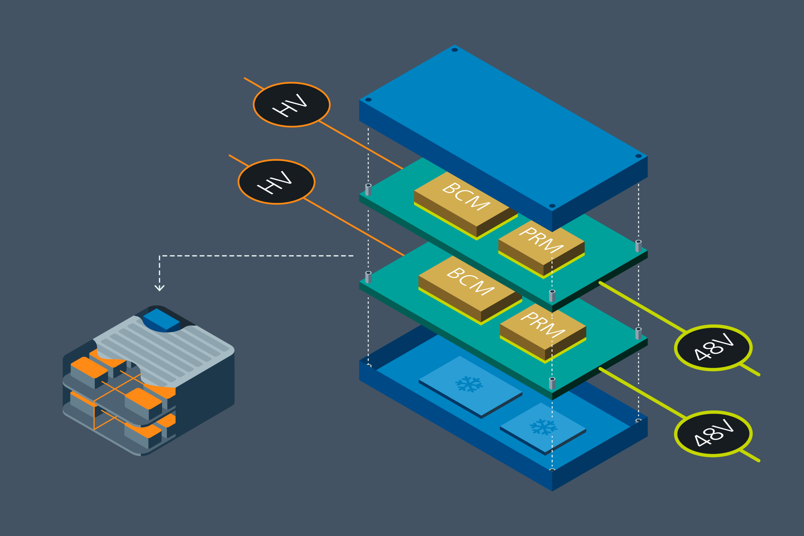
INFAC recognized that traditional approaches to power delivery were misaligned with industry goals for weight reduction, cost optimization and design simplicity.
High voltage DC-DC converters are typically mounted outside the high-voltage (800V or 400V) battery assembly system (BAS), requiring additional safety and thermal management systems. The EV motor and inverter systems demand hundreds of kilowatts of power and require high-voltage wiring harnesses, brackets and enclosures. Other powertrain subsystems and body and chassis electronics require 3.5 – 12kW, and can be easily powered from a 48V SELV zonal power distribution network.
Physically separating the high-voltage source and DC-DC conversion power system unnecessarily duplicates power distribution and management systems, which wastes space, weight and cost and doubles the liquid cooling systems required.
The innovation: Moving DC-DC conversion inside the battery packINFAC’s key insight was that the battery pack already incorporates a robust liquid cooling system for managing thermal loads. By integrating the high voltage DC-DC converter inside the battery, and leveraging the existing infrastructure INFAC eliminated the separate cooling system which traditionally resides outside the battery pack for the DC-DC converter. This departs from conventional “silver-box” design approaches by positioning the battery pack as a central, intelligent power hub rather than a passive energy source.
The change was made using Vicor high-density BCM6135 DC-DC converters and PRM3735 regulators, which provide HV-to-48V conversion and regulation and enable a high-power, fully isolated and regulated bus for the zonal architecture.
Previously, housing the DC-DC conversion function inside the battery pack was impractical as size constraints forced designers to grapple with power management issues, electrical isolation, safety requirements and power module packaging robustness.
Benefits of battery-integrated DC-DC conversionBy co-locating the DC-DC converter within the battery pack, INFAC realized a series of benefits that increased performance at the system level:
- By leveraging the battery’s liquid cooling network, the power module eliminates redundant coolant loops and reduces thermal interfaces.
- High-voltage cable length and thickness are significantly reduced, simplifying high-voltage harness routing and layout.
- Fewer brackets, enclosures and cooling components reduce BOM costs, and weight.
- Minimizing connections and cooling paths reduces leak points and electrical failure risks.
- Fewer external interfaces mean faster, more consistent manufacturing processes.
Vicor high-density, modular power architecture provides the efficiency, scalability and compact form factor required to make battery-integrated 48V distribution practical at scale. In doing so, it positions the battery pack as the central power management and distribution hub for next-generation electric vehicles and enables INFAC to align its EV battery pack designs with the industry’s broader transition toward 48V zonal power architectures.
The post INFAC Develops 800V-to-48V Power Conversion Technology to Targets Higher EV Efficiency appeared first on ELE Times.
🖼 Всеукраїнська виставка «Київ — місто, яке має подобатись»

🖼 У картинній галереї імені Григорія Синиці Центру культури та мистецтв КПІ ім. Ігоря Сікорського відкрилася Всеукраїнська виставка художників та архітекторів «Київ — місто, яке має подобатись».
EPC issues white papers on GaN power conversion for AI data centers and advanced motor drives
Візит задля українсько-японського партнерства

КПІ ім. Ігоря Сікорського прийняв делегацію Палати представників Японії на чолі з її головою Морі Ейсуке, членом Палати представників Масахіто Моріяма, а також Надзвичайним і Повноважним Послом Японії в Україні Осумі Йо разом із представниками Посольства Японії.
Caliptra-enabled hardware security solution eyes AI SoCs

A production-ready root-of-trust and security orchestration solution provides dedicated hardware-level security for mission-critical data center and AI system-on-chips (SoCs). This enterprise-grade solution also accelerates design deployment with a complete hardware and software integration framework that includes dedicated drivers, APIs, and system-level security applications.
Rambus’ CryptoManager Root of Trust provides dedicated hardware-level security in an SoC design by combining a secure RISC-V processor, protected memory, secure key and data storage, cryptographic accelerators, and secure interfaces.
CryptoManager operates alongside an unmodified open-source Caliptra Project core, mediating interactions between the Caliptra Project core, the host processor, and other SoC components. This ensures security-sensitive operations remain within a protected boundary while extending trust across the wider platform.
CryptoManager’s root-of-trust and security orchestration are interoperable with Caliptra, an open-source security framework for silicon root of trust designed for integration into data center-class SoCs. Originally an Open Compute Project (OCP) initiative, it’s currently developed within the CHIPS Alliance.
Caliptra combines hardware, firmware, and specifications to provide a common foundation for device identity, measured boot, and attestation across CPUs, GPUs, AI accelerators, DPUs, networking devices, and other infrastructure components.
“As the Caliptra ecosystem gains momentum, organizations need a practical path to deploy scalable and supportable security solutions in demanding production environments,” said Simon Blake-Wilson, senior VP and GM of silicon IP at Rambus. “CryptoManager Root of Trust supporting the Caliptra specification provides the hardware, software, advanced protections and commercial support needed to accelerate deployment of differentiated enterprise-grade security that is interoperable with the Caliptra framework.”

CryptoManager Root of Trust combines enterprise-grade security with simplified integration and certification readiness for data center and AI SoCs. Source: Rambus
CryptoManager supports classical, post-quantum, and regional cryptographic algorithms. It also provides advanced protections against side-channel and fault-injection attacks, as well as certification support for security standards such as FIPS 140-3 and SESIP.
Furthermore, CryptoManager employs specialized drivers and security applications to offer platform-level awareness, enabling security monitoring, policy enforcement, secure lifecycle management, and coordinated protection of critical system resources.
This platform-wide security awareness, combined with proven side-channel and fault-injection protections, facilitates cryptographic agility for a low-risk path to volume implementations of highly secure data center and AI semiconductor devices.
Related Content
- When AI Meets Hardware Security
- IoT security: Challenges and solutions
- Hardware Root of Trust Essential for AI Chip Integrity
- Hardware security verification must go beyond functional testing
- Hardware Security Requirements for Embedded Encryption Key Storage
The post Caliptra-enabled hardware security solution eyes AI SoCs appeared first on EDN.
Захар Гарник (1998 – 2026)

🇺🇦 Захар Гарник - студент першого курсу Навчально-наукового фізико-технічного інституту КПІ ім. Ігоря Сікорського.
Богдан Канєвський (24.05.1998 – 08.09.2026)

Богдан Канєвський здобув освіту в Навчально-науковому видавничо-поліграфічному інституті КПІ ім. Ігоря Сікорського за спеціальністю «Видавництво та поліграфія». Згодом вступив до аспірантури та викладав на кафедрі репрографії.
КПІ ім. Ігоря Сікорського — переможець конкурсу CampeX з розбудови кампусів досконалості в Україні

🚀 КПІ став одним із 12 університетів — переможців конкурсу CampeX з-поміж 27 учасників за напрямом «Космічні технології».
UK’s Battalion and Penn State launch research collaboration focused on national security
Eggtronic introduces high-efficiency 140W USB-C Power Delivery reference design
🔊 Вступ до кафедри військової підготовки КПІ

На кафедрі військової підготовки КПІ продовжується додатковий набір з підготовки громадян України за програмою підготовки офіцерів запасу за 7 спеціальностями:
Європейський досвід для України: літня академія в Баварії

Асистентка кафедри біоенергетики, біоінформатики та екобіотехнології ФБТ Діна Колтишева цього літа взяла участь у літній академії Баварської адміністрації з охорони навколишнього середовища (Summer academy of the Bavarian environmental administration). Навчання, чи, радше, стажування це проходило в місті Хоф.
SEMI joins ReSiLient consortium to strengthen Europe’s silicon and SiC raw material value chains
VU meter with LM324N Quad op-amps
 | Components required: Breadboard (optional) 1× LM324N 4× 1kΩ Resistors 1× 220kΩ Potentiometer (to adjust reference voltage) 4× LEDs (I'm using random colours because this is a prototype) 1× 220Ω Resistor 5V Supply Earphone Jack (as an input) Some cables and staplers (used by me) Audio Amplifier* wiring diagrams will be posted here, or visit the link in the comment section ^-^ *Connect the input of the VU meter to an audio amplifier with separate power supply [link] [comments] |
Radon sensor embeds sizeable alpha particle detector

PIN photodiode collects, counts, and discriminates alpha energies to determine residences’ radon gas-caused cancer danger degrees.
Back in late July, when I was working on last month’s published piece on radon gas analysis, I longed to see what was inside the battery-operated sensing device I’d recently started using.

But I resisted the temptation to fire up the spudger and screwdriver set, because:
- I’d bought it myself, for $100+, and
- I intended to continue using it long-term, since radon gas concentrations vary over time.
Even if I trusted my ability to disassemble it and then put it back together again in still-full-functional form (which I don’t), I didn’t want to interrupt the data-logging cadence even briefly.
But Providence seemingly intervened on my behalf, as counterbalance to my reticence. Less than a week after my post appeared, a PR contact from Chinese company X-Sense, who swore she hadn’t even seen my coverage yet, reached out to see if I was interested in reviewing its latest consumer-tailored smart radon alarm, the just-introduced XR0A-iR. The device is so new that it only showed up on the company website a few days ago, as I write this on September 10, 2026.


Spooky, eh?


I accepted the invitation with the as-usual qualifiers in such situations: that the company would not see my coverage until it appeared in publicly published form on EDN’s website, and that X-Sense would have no ability to influence the content either in-advance or post-publication. The PR contact agreed.
I also asked for two units; one for hands-on testing (for which I planned to recruit my next-door neighbor, both because he didn’t have one yet and because I wanted to get a non-techie’s take on activation and ongoing use) and the other to satisfy my own teardown curiosity.
Smart equals pervasive data accessX-Sense agreed again. And late last month, two units showed up at my front door. My next-door neighbor successfully activated his yesterday; stay tuned for his hands-on observations to come in a future post. And that same (yester)day, I took the other one apart.
X-Sense is a smart home device manufacturer of which I wasn’t previously aware. The company’s products are analogous to those (for example) of TP-Link, whose Kasa and Tapo temperature, humidity and fluid leak sensors I’ve dissected in recent months. X-Sense already had two radon sensors in its product portfolio, the XR0A-SR and higher-end XR0B-SR, but they’re standalone-use units. The XR0A-iR is its first “connected” radon-related product.
I’ll as-usual start with some outer box shots, accompanied by a 0.75″ (19.1 mm) diameter U.S. penny for size comparison purposes. Top.

Front.

Left side.

Back.

Right side.

And bottom.

The first thing you’ll see after removing the box lid is a comprehensive and consumer-comprehensible (those adjectives rarely get used together, in a positive sense, at least!) user guide.

Underneath it is our patient.

Surrounded by two mysterious baggies.

I jest; they’re not mysterious, because they’re labeled. One, containing silica gel, I commonly encounter to absorb humidity, thereby keeping the electronics dry. The other, marked as indicating that inside it was activated charcoal, was a bit more of an initial head-scratcher.

But then I recalled the mail-in radon lab test (mentioned in my prior writeup) that my wife and I ordered prior to purchasing our home a decade-plus ago, and which looked something like this.

I rattle sound-suspected at the time, and subsequent research has confirmed, that inside it was activated charcoal, used both for short-duration testing and (interestingly, at least to me) for filtering radon out of well water. That said, it’s not recommended for ongoing residential-air radon gas cleansing purposes. Here, I’m guessing, it absorbs ambient radon gas at warehouses and retailer shelves that would otherwise end up on the device’s sensor, adversely affecting subsequent initial-powerup measurement results in the process.
Onward. Here’s our patient, now freed from its previous cardboard captivity. Top (note the grille; hold that thought).

Front.

Left side (note the vents).

Back.

Right (ditto).

And bottom.

Before beginning the dissection, here’s an obligatory company-supplied conceptual image of the supposed “guts”, that I know you all love so much (me too).

The battery compartment often effectively does double-duty as the pathway inside the device. Let’s see if it pans out again.


Those four screw heads, one at each corner, look promising. The unit specs a 2-year (and user-replaceable) battery life claim, by the way. Not too shabby!

Before proceeding, though, let’s zoom in on the always-informative FCC ID (2AU4DDDM).

And now for those pesky screws.


Ladies and gentlemen, we’ve hit the jackpot!


Those white glue deposits at both flex cable-to-connector junctions initially gave me pause. Was I not going to be able to keep this teardown non-destructive, always my preference?


Not so “gluey” after all, it turned out. Never mind. Keep calm and carry on.

Let’s focus our attention first on the top panel and interior of the upper enclosure.

Four more visible screw heads suggest a way to detach the former from the latter. Let’s see.


Bingo!

And now for another perspective, after flipping the enclosure over.

Setting the top panel aside for the moment, we now see that two more screws hold the display assembly in place.

You know what comes next.


And there she goes.


Removing four more screws, I’m betting, will give us a glimpse of the display backside.


I’m on a roll! It’s usually at about this time of inflated self-confidence, by the way, when I short out something, or cut myself and bleed all over everything. Consider yourself warned.


Now for the top panel, and maybe the most baffling aspect of this design. Look back at the earlier top-side overview shot, and you’ll see what appears to be a grille. We already know from the box-bottom notations that this is a passive diffusion design; no (noisy and battery-draining) fans, only natural airflow through the device. Does it flow through the top?
The fact that the documentation only notates the earlier-seen enclosure side vents as “air intake areas” is head-scratching. And when you look at the grille from the inside, you see a black piece of plastic nearly completely covering it. So “nope” is apparently the answer to my question.


So, then, why is it here at all? The earlier-mentioned high-end standalone XR0B-SR model has a speaker up top and behind the grill, for audible-alert purposes.

But it’s also got buttons up top, versus in the front with this particular model, so it’s not like X-Sense can reuse any particular assemblage piece across multiple models.

My only other possible conclusion is that the company is striving to establish a common cosmetic “look” across all models. To wit, ironically, I suspect that the purpose of that black plastic piece is to prevent ambient airflow from going in and/or out the top, forcing it to instead route from one side to the other, presumably over the sensor in the process. Other reader ideas are welcomed in the comments!
Speaking of which, that varying black foam-and-shiny silver plastic circular region up top, held in place by an also-plastic brace, looks promising as a potential radon sensor location.

Let’s see what’s inside it, after first perusing other varying-location perspectives of the overall internal assemblage. Front.

Left side.

Back.

And right side.

I’ve delayed entry, thereby building suspense, more than enough at this point. Here goes nothing.


This looks promising.

We’ve hit pay dirt (although a subsequent Google search on the “CD2026MAR6729” mark wasn’t, alas, even remotely fruitful)!


Upside-down temporary reinsertion into the cavity affords us a closer perspective.

Again, referencing the bottom packaging information, which described the unit’s measurement method as “continuous alpha spectrometry”, this is, I believe (readers?) a solid-state PIN photodiode, described along with other possible implementation approaches in a useful online reference that I came across during my research.
As the acronym suggests, the heavily doped p-type and n-type semiconductor regions, used (among other things) as ohmic contacts, are separated by an intermediary un-doped intrinsic semiconductor region.

The conceptual visual similarity with a multi-pixel image sensor is likely already obvious.

In this case, however, where (i.e. in a particular x:y pixel grid coordinate combination) an alpha particle has struck the semiconductor medium isn’t relevant; that one has struck is all that’s necessary to determine. The sensor normally points downward; the surrounding plastic is obviously no functional impediment. In the following photo, I put the assembly back together so you can see the routing of the seeming single-wire (surprisingly, at least to me) harness out of it.

We still haven’t found the system’s intelligence and wireless connectivity, however. The prior internal assembly front view image suggests there’s a PCB underneath the sensor. Let’s see.


Here it is.


Let’s next see what’s underneath that shiny plastic cover.


A mess of passives (along with a few five-lead ICs, likely single-package dual-transistor devices) is admittedly not what I expected to find. Then again, as I’ve confessed plenty of times before, analog is admittedly not my area of particular expertise.


Two more screws to go.


And the comparatively boring PCB backside is now accessible for visual perusal.


Yawn…unless you’re into switches, test points and/or battery terminals, that is. Let’s give the PCB frontside one more now-standalone look.

The combo 2.4 GHz Wi-Fi plus Bluetooth LE module at left, with a common-frequency, combo-protocol antenna sticking out of it, is the Ai-WB2-32S kit from a previously-unknown-to-me company called AI-Thinker. Is there something explicitly AI-related to this particular product (and/or the manufacturer, more generally)? Or is it just one of those cases nowadays where anything sounds more important if you tack “AI” onto it? The under-Faraday-Cage photo published at the webpage is woefully low-res, but hey, there’s also a spec sheet.

And at center is the system’s processing nexus, the 32-bit Arm Cortex M4-based N32L406MBL7 microcontroller from another new-to-me supplier, Nations Technologies. It has onboard flash memory and SRAM, thereby explaining why I don’t see any discrete memories on the PCB.
Last, but not least, after carefully putting everything back together, the device fired right up.

It’s a miracle!
That’s a wrap for today, folks. As always, reader insights are welcomed in the comments!
—Brian Dipert is the associate editor, as well as a contributing editor, at EDN.
Related Content
- Radon: Level detection, risk determination, and as-needed mitigation
- Improve HVAC efficiency with accurate sensors
- My Geiger counter doesn’t count (sob sob)
- Design femtoampere circuits with low leakage, part 1 and part 2
The post Radon sensor embeds sizeable alpha particle detector appeared first on EDN.
Сторінки




![[link]](https://i.redd.it/3dv6aiiehhph1.jpeg)