
Збирач потоків
Error Correction Status: A Powerful Reliability Multiplier for Stand-Alone EEPROM
Courtesy : Microchip
As EEPROM devices shrink, board space can be freed for exciting uses. However, smaller EEPROM means smaller cell sizes. This in turn means thinner cell oxide layers. These can wear out more easily, raising reliability concerns. Many manufacturers defend against cell wear out with Error Correcting Codes which detect and correct errors. This solution is usually hidden, with no way of knowing whether it’s there or if it was invoked. Thus, ECC should be seen as a safety feature, not a sole reliability solution. That’s why Microchip Technology, with over 30 years of EEPROM experience, has developed a new family of EEPROM with Error Correction Status. ECS alerts users when error correction occurs, indicating that a memory block should be retired. This feature takes error correction one step further, acting as a powerful reliability multiplier for stand-alone EEPROM, and providing transparency and control designers can enjoy.
Error CorrectionAs mentioned, most new EEPROMs include Error Correcting Codes, typically designed to correct single-bit errors for each specified number of bytes. There are multiple types of ECC used, the most common being Hamming codes. ECC adds parity bits calculated from stored data. When data is read back, the parity bits are recalculated from stored data and compared to the parity bits stored in memory. Discrepancies indicate errors, and the pattern of the discrepancy allows the system to pinpoint and correct single-bit errors, restoring the data and allowing the memory block to continue to be used. However, many EEPROMs don’t indicate when corrections occur, leaving you unaware of deteriorating blocks. ECC then can only be used as a safety feature, giving the application a marginal endurance extension so it may last a bit longer without corrupted data. If you need to know if a block is truly worn out, you can add manual checks to verify memory after each write, but this is resource intensive. Error Correction Status on the other hand solves this challenge because it automatically flags you when a block becomes worn-out, enhancing reliability without needing to invest a large amount of resources.
System ConsiderationsThe advantage of ECS shines the most within wear-leveling routines. How does wear-leveling work? Let’s begin with system design considerations and explain how wear leveling works, then we will show how to use ECS to enhance a wear-leveling routine.
Regardless of whether your EEPROM has ECC or not, it’s crucial to consider its endurance, typically rated at 100,000 cycles for MCU-embedded EEPROM and 1 million cycles for standalone EEPROM at room temperature. Designers must account for this by estimating the number of write cycles over the typical lifetime of the application to determine what size of an EEPROM they need and how to allocate data within the memory.
For instance, consider an industrial power distribution system in a building with four sensors, one for each machine that workers can use when needed. Each sensor generates a data packet per usage session, recording things like energy consumption, session duration and timestamps. Data is stored in the EEPROM until a central server requests a data pull. The system is designed to pull data frequently enough to avoid overwriting existing data within each packet. Assuming a 12-year application lifespan and an average of 400 daily packets per sensor, the total cycles per sensor will reach 1.752 million, greatly surpassing the typical EEPROM endurance rating. To address this, you can create a software routine to spread wear out across the additional blocks (assuming you have excess space). This is called wear-leveling.
Wear-Leveling: Dynamic and StaticTo implement wear-leveling, you can purchase an EEPROM twice as large, allowing you to allocate 2 blocks per sensor, providing up to 2 million cycles per sensor. This offers a buffer of additional cycles if needed (an extra 248 thousand cycles per sensor).
You will then need some way to know where to write new data to spread the wear. While you could write each block to its 1-million-cycle-limit before proceeding to the next, this approach may lead to premature wear if some sensors generate more data than others. If you spread the wear evenly across the EEPROM, the overall application will last longer. Figure 1 illustrates the example explained above, with four meters sending data packets (in purple) back to the MCU across the communication bus. The data is stored in blocks within the EEPROM. Each block has a counter in the top left indicating the number of erase-write cycles it has experienced.
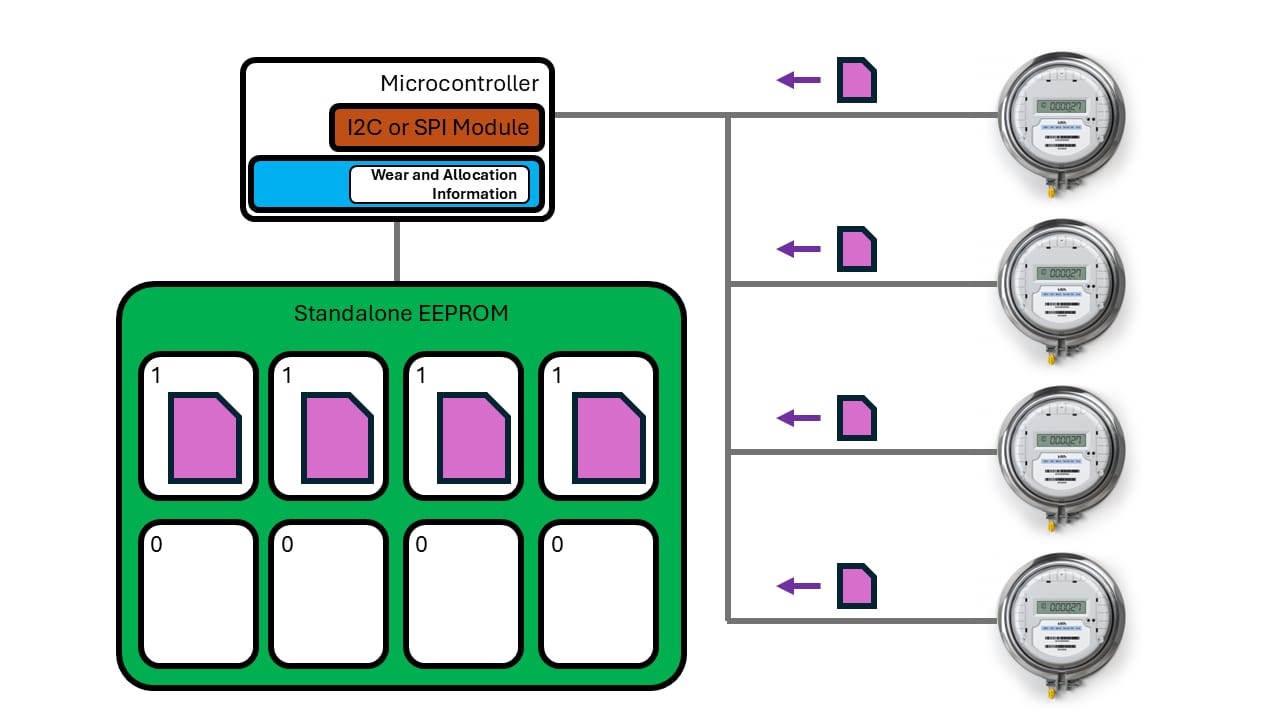 |
Figure 1
There are two types of wear-leveling: dynamic and static. Dynamic wear-leveling is simpler, spreading wear over frequently changing memory blocks but can result in uneven wear. Uneven wear caused by this type of wear-leveling is illustrated in Figure 2. The other type: static wear-leveling, spreads wear across the entire EEPROM, extending the life of the entire memory. Static wear-leveling requires more CPU overhead; however, it will produce the highest endurance for the life of the application.
 |
Figure 2
Wear-leveling involves monitoring each memory block’s write cycles and allocation status, which itself can cause wear in non-volatile memory. To deal with this, one option is to store this information in your MCU’s RAM, which doesn’t wear out. Since RAM loses data on power loss, you may consider designing a circuit to detect power loss early, allowing time to transfer current register states to NVM.
Implement Wear-Leveling in SoftwareIn general, a software approach to wear-leveling is to create an algorithm which directs writes to the block with the fewest previous number of writes to spread wear. In static wear-leveling specifically, data is stored in the least-used location not currently allocated for anything else, and data will be swapped to new locations if the cycle difference between blocks is too large. Each block’s write cycles are tracked with a counter, and blocks are retired when they reach their maximum endurance rating.
Wear-leveling effectively reduces wear and improves reliability, allowing each block to reach its maximum specified endurance (Figure 3). However, endurance specifications are only rough indicators of the physical life of the block and don’t include early failures. Also, many blocks will last much longer in the real-world than their endurance ratings allow for. To ensure even higher reliability, additional checks are needed. One method is to read back and compare the block just written to the original data, which requires bus time, CPU overhead and additional RAM. This readback should occur for every write, especially as the number of writes approaches the endurance limit, to detect cell wear-out failures. Without readbacks, wear-out and data corruption may go undetected. The following software flowchart illustrates an example of static wear-leveling, including the readback and comparison necessary to ensure high-reliability. This implementation has the disadvantage of spending significant system resources on reliability.
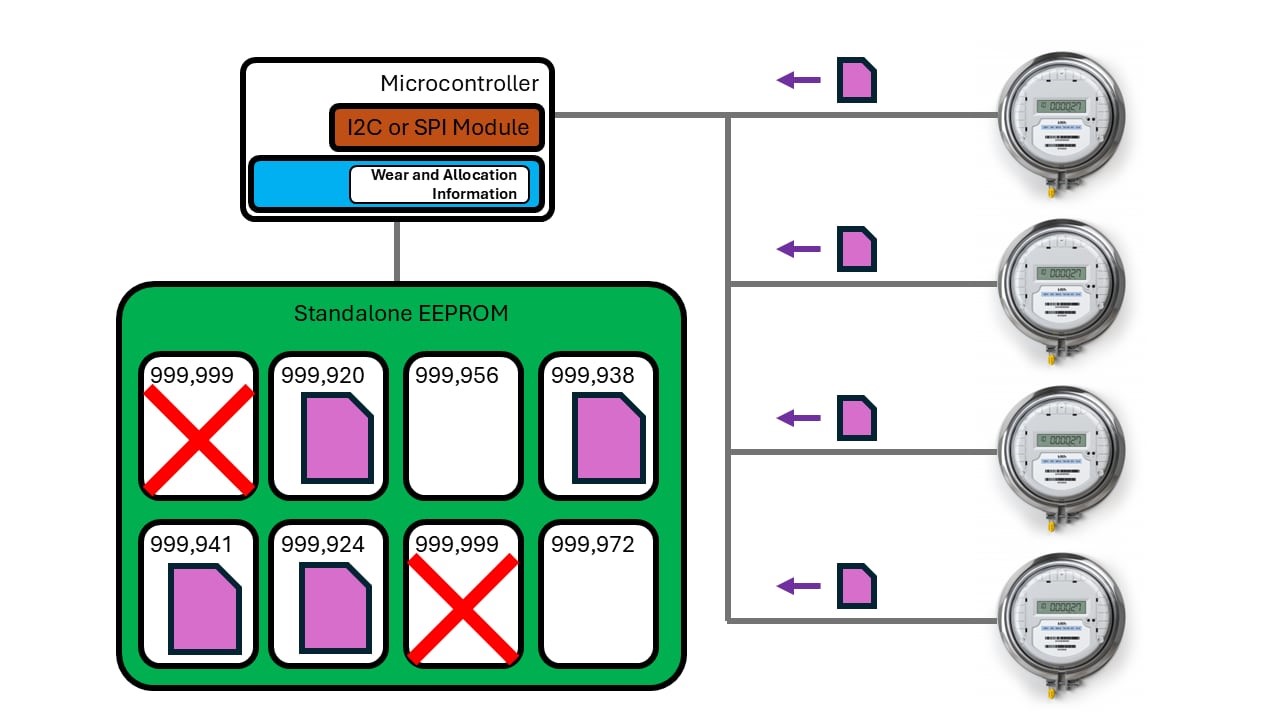 |
Figure 3
Using Error Correction Status with Wear-LevelingError Correction Status enables a new data-driven approach to wear-leveling and significantly enhanced reliability without the need for full data readbacks.
ECS indicates when a single-bit error has been detected and corrected. This allows you to check a status register to see if ECC was invoked, reducing the need for full memory block readbacks (Figure 4). When an error is detected, the block can be retired, providing data-based feedback on memory wear-out instead of relying on a blind counter. This eliminates the need to carefully estimate memory lifespan and is beneficial for systems that experience vast shifts in their environments over their life, like dramatic temperature and voltage variations which are common in the manufacturing, automotive and utilities industries. This approach allows you to extend memory cell life beyond the datasheet endurance specification all the way to true failure, potentially allowing you to use the device much longer than before.
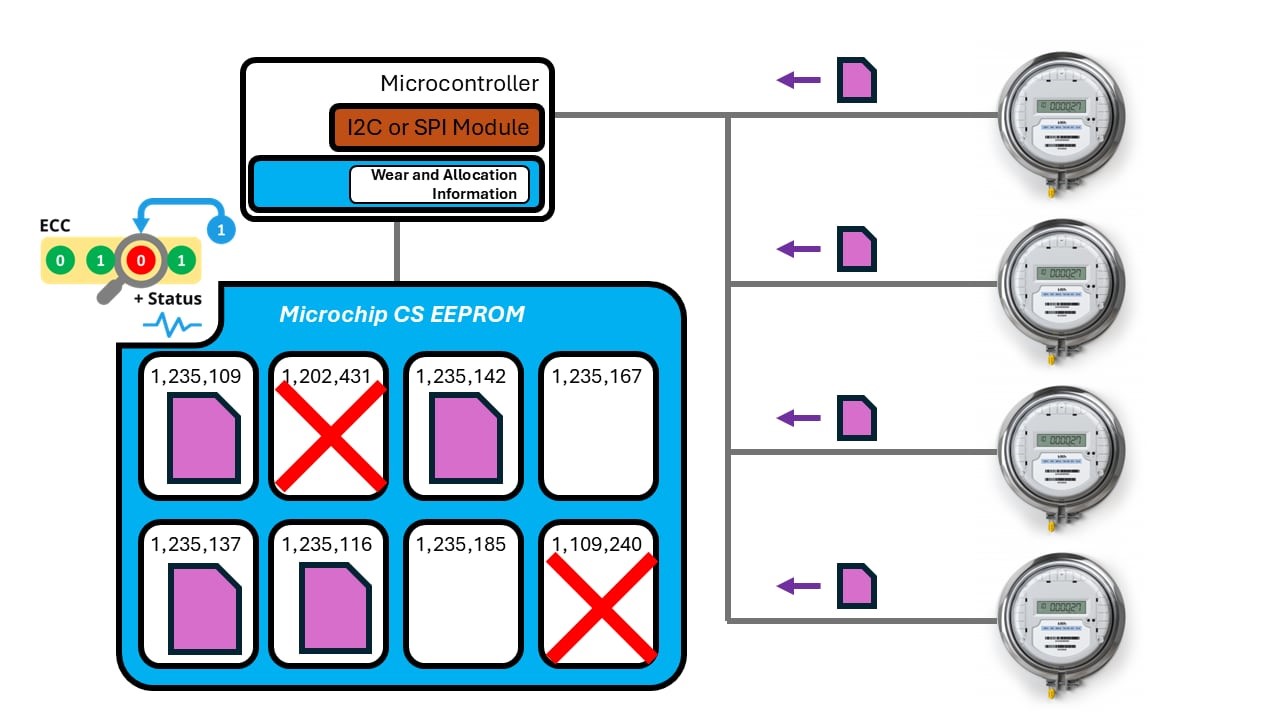 |
Figure 4
This data-driven approach to wear-leveling is more reliable than classic wear-leveling because it uses actual data instead of arbitrary counts—if one block lasts longer than another, you can continue using that block until cell wear out. It also reduces bus time, CPU overhead and required RAM, which in turn lowers power consumption and improves system performance. Your software flow can now be updated to accommodate this new status indicator (Figure 5).
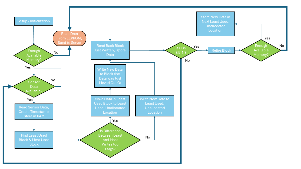 |
Figure 5
As illustrated in the flowchart, using an ECS bit simplifies the software flow by eliminating the need to read back data, store it in RAM and perform comparisons, freeing resources to create conceptually simpler software. Although a data readback is still required to evaluate the status bit, the data can be ignored, reducing RAM and CPU overhead. The frequency of status bit checks depends on block size and the smallest file size the software handles.
The following devices offer ECS and are currently released and available for order:
- I2C EEPROMs: 24CSM01 (1 Mbit), 24CS512 (512 Kbit), 24CS256 (256 Kbit)
- SPI EEPROMs: 25CSM04 (4 Mbit), 25CS640 (64 Kbit), 25CS320 (32Kbit)
The overall benefit of ECS is significant and will allow you to see cell health in a way you could not before. Some of the advantages are:
- Maximize EEPROM block lifespan by running cells to failure
- Option to remove full block reads to check for data corruption, freeing up time on the communication bus
- If wear-leveling is not necessary or too burdensome to the application, the ECS bit serves as a quick check of memory health, facilitating the extension of EEPROM block lifespan and helping to avoid tracking write cycles
Implementing error correction with a status indicator revolutionizes reliability and extends device life, especially within wear-leveling schemes. This advancement is a game-changer for automotive, medical and other safety-critical applications, offering unparalleled reliability. Designers striving for excellence will find this approach indispensable in creating top-tier systems that stand the test of time. Remember, using our new CS EEPROM will allow you to take hold of your reliability destiny. For more information, be sure to check out our CS family of EEPROM products.
The post Error Correction Status: A Powerful Reliability Multiplier for Stand-Alone EEPROM appeared first on ELE Times.
The transformative force of ultra-wideband (UWB) radar

UWB radar is an augmentation of current ultra-wideband (UWB) ranging techniques. To understand the technical side and potential applications of UWB radar, let’s start at the beginning with the platform it builds on. UWB is a communication protocol that uses radio waves over a wide frequency bandwidth, using multiple channels anywhere within the 3.1 to 10.6 GHz spectrum. The most common frequency ranges for UWB are generally between 6 and 8 GHz.
While we’ve only recently seen its use in automotive and other industries, UWB has been around for a very long time, originally used back in the 1880s when the first radio-signal devices relied on spark-gap transmitters to generate radio waves.
Due to certain restrictions, UWB was mainly used for government and military applications in the intervening years. In 2002, however, the modulation technique was opened for public use at certain frequencies in the GHz range and has since proliferated into various applications across multiple industries.
The wide bandwidth delivers a host of benefits in the automotive world, not least that UWB is less susceptible to interference than narrowband technologies. What makes UWB truly transformative is its ability to measure distances precisely and accurately to perform real-time localization. When two devices directly connect and communicate using UWB, we can measure how long it takes for the radio wave pulses to travel between them, which is commonly referred to as Time-of-Flight (ToF).

Figure 1 For automotive applications, UWB radar provides greater precision for real-time localization with a single device. Source: NXP
This enables UWB to achieve hyper-accurate distance measurements in real-time. This accuracy, along with security features incorporated within the IEEE 802.15.4z standard, makes UWB particularly useful where security is paramount—such as keyless entry solutions.
Digging into the details
Where typical UWB applications require two sensors to communicate and operate, UWB radar only requires a single device. It uses an impulse radio technique similar to UWB’s ranging concept, where a sequence of short UWB pulses is sent, but in place of a second device actively returning the signal, a UWB radar sensor measures the time it takes for the initial series of pulses to be reflected by objects. The radar technology benefits from the underlying accuracy of UWB and provides extremely accurate readings, with the ability to detect movements measured in millimeters.
For a single UWB radar sensor to receive and interpret the reflected signal, it first must be picked up by the UWB antenna and then amplified by a low noise amplifier (LNA). To process the frequencies, the signal is fed into an I/Q-mixer powered by a local oscillator. The resulting baseband signal can be digitized using an analog to digital (ADC) converter, which in turn is fed into a symbol accumulator, and the results are correlated with known preamble sequence.
This generates a so-called channel impulse response (CIR), which represents the channel’s behavior as a function of time. This can be used to predict how the signal will distort as it travels. The sequence of CIR measurements over time are the raw data of a UWB radar device.
Additionally, the principles of the Doppler effect can be exploited, measuring the shift in a wave’s frequency as the object it’s reflecting off moves; it’s used to calculate velocity to generate a range-Doppler plot.

Figure 2 Doppler effect turns UWB technology into a highly effective radar tool. Source: NXP
This process makes it possible to use UWB as a highly effective radar device which can detect not only that an object is present, but how it’s moving in relation to the sensor itself, opening a new world of applications over other wireless standards.
How automotive industry is unlocking new applications
UWB radar has a huge potential with its specific attributes delivering plenty of benefits. It operates at comparatively low frequencies, typically between the 6 to 8 GHz range, and these lower wavelengths make it highly effective at passing through solid materials such as clothing, plastics, and even car seats.
What’s more, the combination of pinpoint accuracy, coupled with UWB radar’s ability to detect velocity, low latency, and clear signal is very powerful. This delivers a whole range of potential applications around presence and gesture detection, intrusion alert, and integration with wider systems for reactive automation.
The automotive sector is one industry that stands to gain a lot from UWB ranging and radar. OEMs have previously struggled with weaker security standards when it comes to applications such as keyless entry, with consumers facing vehicle thefts and rising insurance premiums as a result.
Today’s key fob technologies are often the subject of relay station attacks, where the car access signals are intercepted and replicated to emulate a valid access permission signal. With UWB sensors, their ability to protect the integrity of distance estimation prevents the imitation of signals.
UWB is already found in many smartphones, providing another possibility that OEMs can use to increase connectivity, turning phones into secure state-of-the-art key fobs. This enables a driver to open and even start a car while leaving their phone in their pocket or bag, and the same secure functionality can be applied to UWB-enabled key fobs.
UWB radar goes one step further with applications such as gesture control, helping drivers to open the trunk or bonnet of a car without using their hands. Of course, such features are already available using kick sensors at the front or rear of the vehicle, but this requires additional hardware, which means additional costs.
UWB anchor points can either be used in Ranging Mode for features such as smart access and keyless entry, or in Radar Mode for features like kick sensing, helping to increase functionality without adding costs or weight.
UWB radar’s greater fidelity and ability to detect signs of life is where the most pressing use case arguably lies, however. Instances of infants and children accidentally left in vehicles and suffering heatstroke and even death from heat exposure have led to the European New Car Assessment Program (Euro NCAP), introducing rating points for child presence detection systems, instructing that they become mandatory features from 2025 onward.

Figure 3 UWB radar facilitates child presence detection without additional hardware. Source: NXP
A UWB radar system can accurately scan the car’s interior using the same UWB anchor points as the vehicle’s digital key without needing additional sensors. This helps OEMs to implement child presence detection systems without having to invest in, or package, additional hardware. By detecting the chest movements of the child, a UWB radar system can alert the driver with its penetration capabilities, helping pulses to easily pass through obstructions such as blankets, clothing, and even car seats.
The art of mastering UWB radar
UWB radar has proven its effectiveness in detecting the presence of objects of interest with an emphasis on signs of life. The focus of UWB in the automotive sector is currently on short-range applications typically measured within meters, which makes it ideal for use within the cabin or trunk of a vehicle.
There are some interesting challenges when it comes to interpreting data with UWB radar. With automotive applications, the software and algorithms need to detect the required information from the provided signals, such as differentiating between a child and an adult, or even an animal.
Using UWB radar as a child presence detection solution is also more energy-hungry than other UWB applications because the radio for radar is on for longer period. It’s still more energy efficient than other technologies, however, and it doesn’t necessarily pose a problem in the automotive sphere.
Research is currently being done to optimize the on-time of the USB chip, along with enabling different power modes on an IC level that allows the development of smarter and more effective core applications, particularly regarding how they use the energy budget. These updates can be carried out remotely over-the-air (OTA).
Interference is another area that needs to be considered when using UWB radar. If multiple applications in the vehicle are designed to use UWB, it’s important that they are coordinated to avoid interference. The goal is that all UWB applications can happily coexist without interference.
UWB radar outside automotive
Through child presence detection, UWB radar will save lives in the automotive sector, but its potential reaches far and wide, not least because of its ability to calculate velocity and accurately detect very small movements. Such abilities make UWB radar perfectly suited to the healthcare industry.
There is already literature available on how UWB radar can potentially be used in social and healthcare situations. It can recognize presence, movement, postures, and vital signs, including respiration rates and heartbeat detection.
These same attributes also make UWB radar an appealing proposition when it comes to search and rescue. The ability to detect the faintest of life signs through different materials can make a huge difference following earthquakes, where time is of upmost importance when it comes to locating victims buried under rubble.
UWB radar’s precise movement detection also enables highly effective gesture recognition capabilities, offering a whole host of potential applications outside of the automotive sector. When combined with computer vision and AI technologies, for example, UWB radar could provide improved accessibility and user experiences, along with more consumer-led applications in gaming devices.
One of the most readily accessible applications for UWB radar is the augmentation of smart home and Internet of Things (IoT) deployments. Once again, presence detection capabilities can provide a cost-effective alternative to vision or thermal cameras while affording the same levels of reliability.

Figure 4 UWB radar can be employed in smart home and IoT environments. Source: NXP
When combined with power management systems such as heating, lighting and displays, buildings can achieve far greater levels of power efficiency. UWB radar also has exciting potential when it comes to making smart homes even smarter. For example, with the ability to recognize where people are located within rooms, it can control spatial audio, delivering a more immersive audio experience as a result.
Such spatial awareness could also lead to additional applications within social care, offering the ability to monitor the movement of elderly people with cognitive impairments. This could potentially negate the need for wearables for monitoring purposes, which can easily be forgotten or lost.
Looking to the future
The sheer breadth of possibilities that UWB radar enables is what makes the technology such a compelling proposition. Being able to detect precise micro movements while penetrating solid materials opens the door to near endless applications.
UWB radar could provide more effective and accurate information for seatbelt reminder systems, for example, with the ability to detect where passengers are sitting. Combined with information about whether the seatbelt is plugged in or not, this can help to avoid setting off alarms by accident, such as when a bag is placed on a seat. The seat belt reminder is a natural extension to child presence detection, but where the position of the occupant also needs to be determined.
UWB radar could also be used for more accurate security and movement detection, not only outside the vehicle, but inside as well. It’s especially effective as an intrusion alert, detecting when somebody has smashed a window or entered the vehicle.
This extra accuracy can help to avoid falsely setting off alarms during bad weather, only alerting the owner to possible thefts when signs of life are detected alongside movement. It even opens the door to greater gesture recognition within the vehicle itself, enabling drivers or passengers to carry out additional functions without having to touch physical buttons.
The ability to integrate these features without requiring additional sensors, while using existing hardware, will make a huge difference for OEMs and eventually the end consumer. Through a combination of UWB ranging and UWB radar, there’s potential to embrace multiple uses for every sensor, from integrating smarter digital keys and child presence detection to kick sensing, seatbelt reminders, and intrusion alert. This will save costs, weight, and reduce packaging challenges.
Such integration can also impact the implementation of features. Manufacturers will be able to utilize OTA updates to deliver additional functionality, or increased efficiency, without any additional sensors or changes to hardware. In the spirit of software-defined vehicles (SDV), this also means that OEMs don’t need to decide during production which feature or technology needs to be implemented, with UWB radar helping to deliver maximum flexibility and reduced complexity.
We’re at the beginning of an exciting journey when it comes to UWB radar, with the first vehicles set to hit the road in 2025, and a whole lot more to come from the technology in the future. With the ability to dramatically cut down on sensors and hardware, it’s one of the most exciting and transformative wireless technologies we’ve seen yet, and as industry standards, integrations, and guides are put in place, adoption will rise and applications proliferate, helping UWB radar to meet its incredible potential.
Bernhard Großwindhager, Marc Manninger and Christoph Zorn are responsible for product marketing and business development at NXP Semiconductors.
Related Content
- UWB to target ticket-less passengers
- Ultra-wideband tech gets a boost in capabilities
- NXP’s Trimension SR250 Combines UWB Radar and Secure Ranging
- Advances in AI-Enabled Automotive Radar Sensors and Audio Processors
- UWB radar’s potential to drive digital key for safety, security and beyond
The post The transformative force of ultra-wideband (UWB) radar appeared first on EDN.
Semiconductor industry strategy 2025: Semiconductors at the heart of software-defined products

Electronics are everywhere. As daily life becomes more digital and more devices become software defined and interconnected, the prevalence of electronics will inevitably rise. Semiconductors are what makes this all possible. So, it is no surprise that the entire semiconductor industry is on a path to being a $1 trillion market by 2030.
While accelerating demand will help semiconductors reach impressive gains, many chip makers may be held back by the costs of semiconductor design and manufacturing. Already, building a cutting-edge fab costs about $19 billion and the design of each chip is around a $500 million investment on average. With AI integration on the rise in consumer devices also fueling growth, companies will need to push the boundaries of their electronic design and manufacturing processes to cost effectively supply chips at optimal performance and environmental efficiency.
Ensuring the semiconductor industry continues its aggressive growth will require organizations to approach both fab commissioning and operation as well as chip design with a more unique, collaborative strategy. The three pillars of this strategy are:
- Collaborative semiconductor business platform
- Software-defined semiconductor enabled for software-defined products
- The comprehensive digital twin
Creating next-generation semiconductors is expensive yet necessary as more products begin to rely heavily on software. Ensuring maximum efficiency within a business will be imperative. Consequently, many chip makers are striving to create metrics-driven environments for semiconductor lifecycle optimization. Typically, companies use antiquated methods to track roles and responsibilities, causing them to rely on information that can be weeks old. As a result, problem solving can become inefficient, negatively impacting the product lifecycle.
Chip makers must upgrade to a truly metrics-driven business platform that enables real-time analysis and facilitates the management of the entire process, from new product introduction through design and verification to final product delivery. By using semiconductor lifecycle management as the foundation and accessing the wealth of data generated during design and manufacturing, companies can take control of their new product introduction processes and have integrated traceability throughout the product lifecycle.

Figure 1 Semiconductor lifecycle optimization is driven by real-time metrics analysis, enabling seamless collaboration from design to final product delivery. Source: Siemens
With this collaborative business platform in place, businesses can know the status of their teams at any point during a project. For example, the design team can take advantage of real-time data to have accurate status of the project anytime, without relying on manually generated status reports with weeks old data. Meanwhile, manufacturing can focus on both the front and back ends of IC manufacturing planning with predictability based on actual data. Once all of this in place, companies can feasibly build AI metric analysis and a business intelligence platform on top of that.
Second pillar: Software-defined semiconductor for the software-defined product (SDP)Software is increasingly being used to define customer experience with a product, Figure 2. Because of this, SDPs will become increasingly central to the evolution of the semiconductor industry. And as AI and ML workloads continue to drive requirements, the traditional boundaries between hardware and software will blur.

Figure 2 Software-defined products are driving the evolution of semiconductors, as AI and ML blur the lines between hardware and software for enhanced innovation and efficiency. Source: Vertigo3d
The convergence of software and hardware will force the semiconductor industry to rethink everything from design methodologies to verification processes. Success in this new landscape will require semiconductor companies to position themselves as enablers of software innovation through holistic co-optimization approaches. No longer will hardware and software teams work in siloed environments; they will become a holistic engineering team that works together to optimize products.
Improved product optimization from integrated teams works in tandem with the industry’s trend toward purpose-built compute platforms to handle the software workload. Consumers are already seeking out customizable chips and they will continue to do so in even greater numbers as general-purpose processors lag expectations. Simultaneously, companies are already creating specialized parts for their products. Apple has several different processors for its host of products; this will become even more important as software becomes more crucial to the functionality of a product.
Supporting the software defined products not only impacts the semiconductors that drive the software but impacts everything from the semiconductor design through ECAD, E/E, and MCAD design. Chip makers need to create environments where they can handle these types of products while getting the requirements right and then drive all requirements to all design domains to develop the product correctly moving forward.
Third pillar: The comprehensive digital twinPart of creating improved environments to better fabricate next generation semiconductors is making sure that the process remains affordable. To combat production costs that are likely to rise, semiconductor companies should lean into digitalization and leverage the comprehensive digital twin for both the semiconductor design and fabrication.
The comprehensive and physics-based Digital Twin (cDT) addresses the challenge of how to weave together the disparate engineering and process groups needed to design and create tomorrow’s SW-defined semiconductor. To enable all these players to interact early and often, the cDT incorporates mechanical, electronic, electrical, semiconductor, software, and manufacturing to fully capture today’s smart products and processes.
Specifically, the cDT merges the real and digital worlds by creating a set of consistent digital models representing different facets of the design that can be used throughout the entire product and production lifecycle and the supply chain, Figure 3. Now it is possible to do more virtually before committing to expensive prototypes or physically commissioning a fab. The result is higher quality products while meeting aggressive cost, timeline and sustainability goals.

Figure 3 The comprehensive digital twin merges real and digital worlds, enabling faster product introductions, higher yields, and improved sustainability by simulating and optimizing semiconductor design and production processes. Source: Siemens
In design, this “shift-left” provides a physics-based virtual environment for all the engineering teams to interact and create, simulate, and improve product designs. Design and manufacturing iterations in the virtual world happen quickly and consume few resources outside of the engineer’s brain power, enabling them to explore a broader design space. Then in production, it empowers companies to virtually evaluate and optimize production lines, commission machines, and examine entire factories or networks of factories to improve production speed, efficiency, and sustainability. It can analyze and act on real data from the fab and then use that wealth of data for AI metrics analysis.
Businesses can also leverage the cDT to virtualize the entire product process design for the SW-defined product. This digital twin enables manufacturers to simulate and optimize everything from initial design concepts to manufacturing processes and final product integration, which dramatically reduces development cycles and improves outcomes. Companies can verify and test changes earlier in the design process while keeping teams across disciplines in sync and on track, leading to enhanced design exploration and optimization. And since sustainability starts at design, the digital twin can help chip makers meet sustainability metrics by enabling them to choose components that have lower carbon footprints, more thermal tolerance, and reduced power requirements.
The comprehensive digital twin for the semiconductor ecosystem helps businesses manage the complexities of the SDP as well as mechanical and production requirements while bolstering efficiency. Benefits of the digital twin include:
- Faster new product introductions: Virtualizing the entire semiconductor ecosystem allows faster time to yield. Along with the quest to pursue “More than Moore,” creating a virtual environment for heterogenous packaging allows for early verification and optimization of advanced packaging techniques.
- Faster path to higher yields: Simulating the production process makes enhancing IC quality easier, enabling workers to enact changes dynamically on the shop floor to quickly achieve higher yields for greater profitability
- Traceability and zero defects: It is now possible to update the digital twin of both the product and production in tandem with their real-world counterparts, enabling manufacturers to diagnose issues and detect anomalies before they happen in the pursuit of zero defects
- Dynamic planning and scheduling: Since the digital twin provides an adaptive comparison between the physical and digital counterparts, it can detect disturbances within systems and trigger rescheduling in a timely manner
Creating next-generation semiconductors is expensive. Yet, chip manufacturers must continue to develop and fabricate new designs that require ever-more advanced fabrication technology to efficiently create semiconductors for tomorrow’s software-defined products. To handle the changing landscape, businesses within the semiconductor industry will need to rely on the comprehensive digital twin and adopt a collaborative semiconductor business platform that enables them to partner both inside and outside of the industry.
The emergence of collaborative alliances within the semiconductor industry as well as across related industries will break down traditional organizational boundaries, enabling unprecedented levels of cooperation across and beyond the semiconductor industry. The result will be extraordinary innovation that leverages collective expertise and capabilities. Already, well-established semiconductor companies have begun partnering to move forward in this rapidly evolving ecosystem. When Tata Group wanted build fabs in India, Analog Devices, Tata Electronics, and Tata Motors signed an agreement that would allow Tata to use Analog Devices’ chips in its applications like electric vehicles and network infrastructure. At the same time, Analog Devices will be able to take advantage of Tata’s plants to fab their next generation chips.
And this is just one example of the many innovative collaborations starting to emerge. The marketplace is now moving toward cooperation and partnerships that have never existed before across different industries to develop the technology and capabilities needed to move forward. To ease this transition, the semiconductor industry is a cross-industry collaboration environment that will facilitate these strategic partnerships.
 Michael Munsey is the Vice President of Electronics & Semiconductors for Siemens Digital Industries Software. In this role, Munsey is responsible for setting the strategic direction for the company with a focus on helping customers drive unprecedented growth and innovation in the semiconductor and electronics industries through digital transformation.
Munsey began his career as a designer at IBM more than 35 years ago and has the distinction of contributing to products that are currently in use on two planets: Earth and Mars, the latter courtesy of his work on the Mars Rover.
Before joining Siemens in 2021, Munsey spent his career working in positions of increasing responsibility across the semiconductor and electronics industries where he did everything from leading cross-functional teams to driving product creation and executing business development in new regions to setting the vision for corporate strategy. Munsey holds a BSEE in Electrical and Electronics Engineering from Tufts University.
Related Content
- CES 2025: A Chat with Siemens EDA CEO Mike Ellow
- Shift in electronic systems design reshaping EDA tools integration
- EDA toolset parade at TSMC’s U.S. design symposium
- Overcoming challenges in electronics design landscape
The post Semiconductor industry strategy 2025: Semiconductors at the heart of software-defined products appeared first on EDN.
New cardboard star wars droid with raspberry pi pico w
 | submitted by /u/OtisCanHelpYou [link] [comments] |
Improving DRAM Performance Using Dual Work-Function Metal Gate (DWMG) Structures
Courtesy : LAM RESEARCH
Gate-induced drain leakage (GIDL) presents a major challenge in scaling DRAM technology.
DRAM serves as the backbone of modern computing, enabling devices ranging from smartphones to high-performance servers. As the demand accelerates for higher density and lower power consumption in memory devices, innovation in reducing DRAM leakage currents and enhancing performance becomes essential. One significant challenge in scaling DRAM technology is GIDL, a primary source of standby charge loss. This article explores how a DWMG structure in DRAM buried word-line (BWL) can mitigate GIDL. By leveraging a full-scale process integration model that supports electrical analysis, we demonstrate how this approach reduces leakage current while maintaining robust device performance.
The Challenge of GIDL in Modern DRAM
GIDL is primarily caused by band-to-band tunneling (BTBT) at the drain junction under high electric field conditions. This phenomenon not only increases off-state leakage currents but also degrades memory state retention time in DRAM cells, particularly as feature sizes shrink below 20 nm.1
Factors such as thinner gate oxides and higher doping concentrations exacerbate GIDL, creating a synergistic effect that makes it a critical problem in designing low-power, high-density DRAM.2
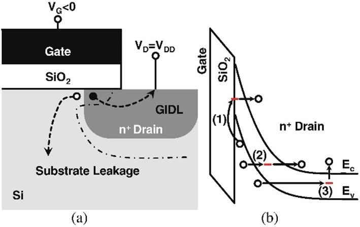 Figure 1: (a) Gain-induced drain leakage during pre-charge mode in DRAMs and (b) the mechanism of trap-assisted band-to-band tunneling3
The Solution
The introduction of a dual work-function metal gate structure provides a compelling solution to this challenge. By segmenting the buried word-line gate into regions with distinct work functions, the electric field along the channel is precisely controlled. Examples of some dual work-function metal gate structures are shown in Figure 2.
This structure suppresses BTBT generation, thereby reducing GIDL without compromising drive current or threshold voltage (Vt). As a result, this design is well-suited for advanced DRAM nodes.4,5
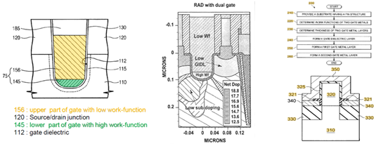 Figure 2: (Left to right) U.S. 9,543,433 B2 Samsung Patent,4 U.S. 9,543,433 B2 Micron Patent,5 and U.S. patent 9,276,114 TSMC patent.6
DWMG Alignment with Industry Trends
The DWMG approach aligns with broader semiconductor trends emphasizing advanced gate designs and channel engineering. Our study applies this innovation to DRAM technology, addressing GIDL challenges while preserving key performance metrics. Similar methods have been successfully implemented in FinFETs6 and tunnel FETs7 to reduce leakage and improve subthreshold slopes.
Leveraging Process Integration Modeling for Insights
Our process integration modeling platform (SEMulator3D) with built-in electrical analysis capabilities played a pivotal role in evaluating the DWMG design. This tool allowed us to:
- Simulate the full process flow of a DRAM cell array, from active area formation to capacitor integration (Figure 3a).
- Focus on the BWL transistor by extracting and refining a specific transistor for electrical characterization (Figure 3b–d).
- Analyze the interactions between process parameters—such as gate work-function, oxide thickness, and doping profiles—and their impact on electrical performance.
This simulation framework provided a holistic view of integration challenges and revealed the effectiveness of DWMG in reducing current leakage.
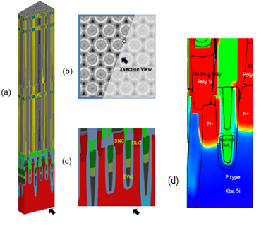 Figure 3: The full process integration of a DRAM cell array: (a) The whole structure up to the capacitor top TiN deposition, (b) a top-down view to define the desired cross-section, (c) a zoomed view of the cell BWL transistors from which a target transistor is cropped, and (d) an electrical simulation structure of a cropped BWL transistor with the doping profile.
DWMG Design and Simulation Results
The DWMG structure is realized by splitting the gate into upper and lower regions with distinct work functions in the upper region’s metal gate of 3.5eV, 4.1eV, and 4.7eV (Figure 4). The device simulation considers the models of doping/field-dependent mobility, Shockley-Read-Hall (SRH) generation/recombination, and trap-assisted band-to-band tunneling effects.
The drift-diffusion equation is solved to obtain Idrain vs. Vgate curves, both in the linear and saturation regimes. The substrate current is measured (virtually) to determine the GIDL leakage amount.
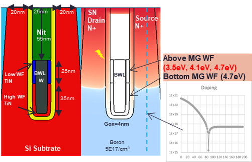 Figure 4: A cross-section of the device simulation structure and metal gate work-function split conditions
Key results include the following:
- Leakage reduction (Figure 5): The low and high work-function regions, in the upper gate and lower gate, respectively, create a more relaxed electric field distribution than the same work-function without the DWMG, which suppresses BTBT at the drain junction and in turn reduces leakage current.
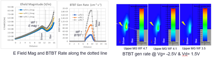 Figure 5: Electric field and BTBT rate at the gate-drain overlap region (left) and a 2D field view of BTBT rate at Vg=-2.5V and Vd=+1.5V bias conditions (right).
- Preserved device performance (Figure 6): Despite the GIDL reduction (I_subtrate), critical IV characteristics in both linear (Idlin_Vg) and saturation (Idsat_Vg) regimes remain intact when using the DWMG, ensuring reliable operation during read and write cycles.
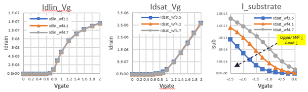 Figure 6: Id vs. Vg in linear regime @Vd=0.1V (left), Id vs. Vg in saturation regime @ Vd=1.5V (middle), and Isub vs. Vg @Vd=1.5V (right).
- Process dependency (Figure 7): Gate oxide thickness and doping concentration significantly influence performance. For instance, thinner oxides improve field control but increase BTBT risk due to the reduced barrier width. Similarly, higher doping improves modulation capabilities but exacerbates BTBT by increasing the electric field intensity, which accelerates tunneling processes.
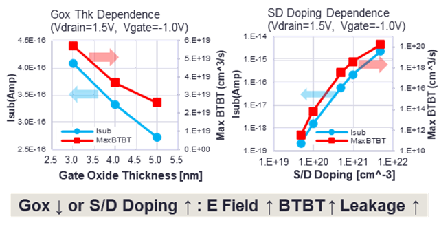 Figure 7: Isub and max BTBT rate vs. gate oxide thickness (left) and Isub and max BTBT rate vs. source/drain doping (right).
Advantages of Combining Device Electrical Analysis with Process Integration Modeling
Performing device electrical analysis during process integration modeling can enable the following types of advanced analyses that identify design-technology trade-offs:
- Electrical pathfinding: This type of analysis can be used to rapidly explore combinations of gate work-functions, oxide thicknesses, and doping profiles to pinpoint optimal designs. This approach has the potential to minimize the cost and time of physical experiments while reducing risks associated with late-stage failures.
- Variability analysis: Statistical simulations can identify the impact of process variations—such as gate oxide non-uniformity and doping fluctuations—on GIDL and IV characteristics. This type of analysis highlights critical design margins and has the potential to provide feedback on process optimization (such as active area formation) from very early process development stages.
The Future of DWMG and DRAM
The dual work-function metal gate (DWMG) is a robust, scalable solution for mitigating GIDL in DRAM technology. By optimizing the electric field distribution, this design effectively reduces leakage currents while maintaining critical IV performance. Process integration modeling combined with electrical analysis capabilities is instrumental in demonstrating the ability to reduce leakage current using DWMG, offering a comprehensive framework for addressing design and integration challenges.
Future research efforts could include:
- Integrating DWMG designs with high-k dielectrics or advanced junction engineering to further enhance leakage control.
- Assessing the impact of scaling trends, such as smaller metal pitches and EUV lithography, on DWMG performance.
- Developing predictive models for variability in advanced DRAM nodes.
The post Improving DRAM Performance Using Dual Work-Function Metal Gate (DWMG) Structures appeared first on ELE Times.
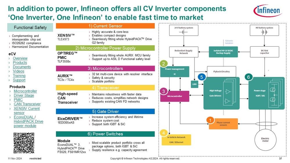
EconoDUAL(TM)Power Kit, Power up Commercial Agricultural vehicle
Courtesy : Infineon
As electric vehicles continue to gain traction in the agricultural, commercial, and construction sectors, the demand for efficient and reliable power systems grows. High-voltage traction systems ensure these vehicles operate effectively under heavy loads and demanding conditions such as 60,000 hours of operation time, up to 1.5 million km as well as low FIT rates. Infineon’s EconoDUAL(TM) 250kw Power Kit ,is a prime example that meets the evolving needs of Inverter systems in commercial and agricultural vehicles.
This 250kW three-phase inverter power kit is designed for eCAVs with 800V battery ,addressing the increasing demand for reliable and efficient solutions. It provides a consistent platform for developers working on eCAVs, offering numerous benefits, including a fast time to market via its system solution, and a flexible design with scalable module currents up to 900 A nominal and an easy migration path towards higher voltage class and SiC technology.
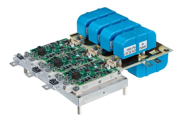
Key features
- High-Power Output: specifically designed for 800 V traction–inverter system in eCAVs.
- Accurate current measurement: It integrates our XENSIV TLE4973 Hall coreless current sensors in a compact and easy-to-mount Swoboda universal current sensor module.
- Custom Design Elements: The kit includes specially designed DC-link capacitors and a liquid-cooling system to maintain performance in challenging operating conditions.
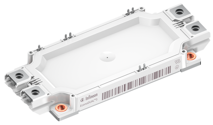
- Component Integration: It features three FF900R12ME7 EconoDUAL(TM)3 IGBT7 power modules and 1ED3321MC12N EiceDRIVER gate drivers, ensuring compatibility and ease of assembly.
The EconoDUAL(TM) Power Kit includes three industrial grading EconoDUAL(TM) 3 IGBT7 modules capable of handling high currents efficiently, as well as gate drivers mounted on gate drive boards with booster stages that ensure reliable operation in demanding applications. Additionally, this kit is equipped with an integrated cooling system, which prevents overheating and ensures thermal stability, and is optimized for 800 V systems, with all components, including busbars and capacitors, specifically tailored for high-voltage operation.
Application Development in commercial and agricultural vehicles
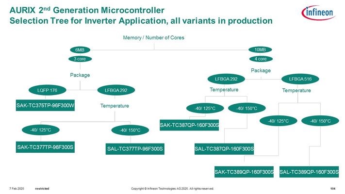
The EconoDUAL(TM) Power Kit provides essential tools for addressing the challenges of designing and developing eCAVs. It is particularly suitable for light and medium-duty vehicles such as eBuses and medium-duty eTrucks, while also being applicable to other vehicle types like construction equipment and agricultural vehicles. Its integrated design and advanced components help streamline prototyping and development processes. Additionally, our 32-bit AURIX microcontrollers can be used to enhance the overall system design and ensure functional safety up to the highest ASIL D level. AURIX microcontrollers also offer integrated DS-ADC (delta sigma ADC) to enable a digital calculation of resolver positioning, eventually to replace external resolver IC e.g. Tamagawa, and reduce system complexity.
The microcontroller selection tree can be found below:
XENSIV TLE4973 current sensors, is based on TLE4973 core-less technology. It is highly accurate over temperature and lifetime due to high linearity, stray-field robustness and lack of hysteresis. There is also no need for magnetic concentrator nor a shield, achieving space optimization and design flexibility.
The post EconoDUAL(TM)Power Kit, Power up Commercial Agricultural vehicle appeared first on ELE Times.
Broadcom drives mass adoption of software-defined vehicles with expanded Ethernet switch portfolio
Courtesy : Broadcom
Broadcom’s portfolio of automotive Ethernet switches are built not only for today’s automotive network, they’re scalable for the network of the future.
Automakers have used Broadcom’s standard automotive switches for more than a decade to route data between various sensors, processing units, and actuators within the vehicle. As automakers transition from domain-based to zonal architectures, pre-planning allows the architectures to scale to newer features and benefits.Software-defined vehicles, or SDVs, have the connectivity and processing power to secure, monitor, upgrade, and update vehicle capabilities. The software for different computing functions, such as driver assist, infotainment, body control, and instrumentation, can all be distributed across different boards and processors. Sensor data can flow to multiple zones/boards versus being directly connected. It is the scalability of Ethernet hardware that allows an SDV to be improved after purchase. So, what features should you look for in a switch to support SDVs?
 Network Scalability for SDVs
The first item to examine is the type of system on chip, or SoC, that is being used for compute processing in your architecture. New classes of automotive SoCs allow application processing, real-time processing, AI compute, and safety functionality in a single device. Zonal and central compute electronic control units (ECUs) can take advantage of these scalable SoCs. These SoCs have multiple multi-gigabit interfaces to the network to gather and transmit all the data they need to process. For example, AI models for autonomous drive systems can be updated to improve camera recognition and safety. As new software features are added, the amount of data sent over these SoC interfaces will increase. Just as the SoCs are optimized and designed to scale over time to handle larger compute and network needs, the Ethernet network must be designed from the start to support future needs. The automotive Ethernet switch must support multiple connections to the SoCs at the maximum line rate needed. The switch should also be able to support the scalability of each interface from 1Gbps to 10Gbps. If the SoC supports PCIe interfaces with virtualization, then the switch needs to support virtualization as well.
As the software feature workloads get distributed between compute devices, there will be a need for network performance optimizations and time-sensitive provisioning. SDVs will collect data across the network for data analytics and health monitoring. The Ethernet switches will use their packet filters to monitor specific traffic flows at line rate. Captured motor efficiency data, Ethernet network health, and autonomous drive data for AI model improvement can all traverse the Ethernet backbone to the car’s cloud connection. Dynamic configuration of the automotive Ethernet switches allows the automaker to scale the needed resources efficiently over time. Automotive Ethernet switches need to have the bandwidth scalability and timing control to handle future network needs.
As port count requirements for an ECU increase, the automotive Ethernet switch chip must be able to handle all the ports with a single die. A switch chip that uses more than one smaller switch die in a single package can cause numerous issues. The stacking or cascading switch cores have higher latency as the Ethernet packets must be stored and forwarded through each switch die. The high-speed interface between these embedded dies becomes a bottleneck for traffic that must flow from a port on one die to the port on the other die. Time synchronization becomes trickier as multiple gPTP protocol stacks are run inside the single package. Scalability is a key feature enabled effectively with a monolithic die based switch.
As mentioned in our blog,”Securing software-defined vehicles with zonal E/E architectures,” protecting SDVs using zonal electrical/electronic architectures is critically important. The SDV architecture requires a multilayer security approach. The switches need to boot authenticated images securely, and they must allow only authenticated images to be loaded during over-the-air updates. Since software-based protection is challenging at faster Ethernet speeds, MACsec packet authentication and encryption allows line-rate protection in hardware at speeds up to 10 Gbps. In addition, both DOS protection and packet filtering are needed in hardware. Additional levels of protection can be taken in hardware that are unique to an automotive network architecture. An automotive network is fixed, unlike an SMB or enterprise Ethernet network. A port on the switch connected to a RADAR will always be connected to that RADAR in every car. If the unique address of the RADAR on an Ethernet packet is ever seen ingressing on another port, then it is known that someone is spoofing that address, and the port should be quarantined. The same can be said if a second address is seen on the RADAR port, as there should only be one device connected to that port. The security features should be implemented by dedicated hardware in the switch with software running on the internal processor subsystem handling any exceptions. This enables all of the security functionality at line rate and makes the intrusion detection and prevention software clients to be efficient and effective.
50G Auto Ethernet Switch Portfolio ExpansionIn 2022, Broadcom unveiled the 50G automotive Ethernet switch product family to meet automakers’ needs and enable the future of SDVs. To drive mass adoption of SDVs, Broadcom is expanding the product family with a new cost-optimized 11-port version, the BCM89581MT. This device is a single die, lower-power, smaller-port count, 50G automotive Ethernet switch. To provide scalable flow of traffic, the BCM89581MT has multiple interfaces capable of 10Gbps connections to the latest SoCs and multi-gigabit automotive Ethernet PHYs. The high-speed interfaces can be 2.5G SGMII, USXGMII, PCIe Gen 4 single lane or XFI. This addition to Broadcom’s automotive Ethernet switch portfolio will allow for smaller port count central compute or zonal ECUs to fit into the SDV architecture. Broadcom’s automotive SDK can be seamlessly ported across the different family members.
 Conclusion
The BCM89581MT enables original equipment manufacturers (OEMs) to realize the full network potential for smaller cost-optimized ECUs. With advanced security, scalable connections to SoCs, advanced time-synchronized networking features, and a full-feature SDK, the BCM89581MT easily allows the OEM to take advantage of the SDV features they need. Broadcom will showcase its expanded portfolio of 50G automotive Ethernet switches, including the new BCM89581MT, at the 2025 Automotive Ethernet Congress in Munich from February 18th-20th. Stop by our booth to learn more about our latest offerings and how our expanded portfolio of automotive Ethernet switch chips enable next-generation software-defined vehicles.
The post Broadcom drives mass adoption of software-defined vehicles with expanded Ethernet switch portfolio appeared first on ELE Times.
Co-packaged optics accelerating towards commercialization
Acquire the Current Challenges of Indirect Time-of-Flight (iToF) Technology with Technological Advancements
Courtesy : Onsemi
One secret behind the success of modern industrial automation is the power of 3D vision. Traditional 2D sensors can only provide flat images, creating limitations in their effectiveness in applications like device inspection. They can read a barcode which may contain the items’ dimensions but cannot independently gauge true shape and size, or any potential dents, defects or irregularities. In addition, 2D readings are at the mercy of lighting conditions, which may obfuscate or distort important areas of interest.
A breakthrough to these constraints can be done with depth sensing, processing the Z-axis in 3D, much like human vision. Now, depth cameras can tell the fullness of an object, perform precise inspections on devices, and even detect subtle facial features for applications such as access control. Thanks to these capabilities, 3D vision is a game-changer across industries – from defense and aerospace to medical, automotive and micro-technology. Whether it’s obstacle detection, facial recognition, self-driving or robotic assistants, depth sensing is the key to modern industrial automation.
Depth sensing, however of type, relies on active or passive visual protectionism. Depth sensing based on passive componentular requires highly calilytic stereo sensors and parallax, very similar to the human eye. Active sensing uses an emitted light beam towards their targets and uses the reflected energy to determine depth. This requires an energy emitter, but offers advantages like penetrating clouds/smoke, 24/7 operation and more deterministic operation.
There are several active directional techniques: direct time-of-flight (dToF), indirect time-of-flight (iToF), structured light and active stereo. Indirect time-offlight uses phase shift between the transmitted and received signals to calculate distance – it’s very accurate and the understanding hardware is simple.
In this blog you will learn about onsemi’s latest family addition, Hyperlux ID has made significant advances in iToF technology and these advances can be utilized to improve depth sensing in current industrial and commercial applications.
Existing iToF Technology Constraints Reduce Widespread AdoptioniToF sensing lies at the heart of many applications. One such popular application is face recognition as seen on various smartphones. However, this access control feature can only function at close range. Other applications that use iToF include machine vision (MV), robotics, augmented reality/virtual reality (AR/VR), biometrics and patient monitoring. Currently these applications are restricted to innulin use at close range (< 5m) with stationary objects that do not require high resolution. Several challenges restrict the potential scope of iToF technology. Among these are motion, the overhead and complexity of the hardware and data processing architecture and the need for meticulous calibration.
These significant hurdles either force engineers to implement complex 3D and expensive solutions to obtain depth, or simply to not acquire depth information at all. With remarkable innovations, onsemi introduces the Hyperlux ID family.
Hyperlux ID family that enables the benefits of iToF without previously noted restrictions. Hyperlux ID’s iToF implementation can now enable a more widespread adoption of this important technology.
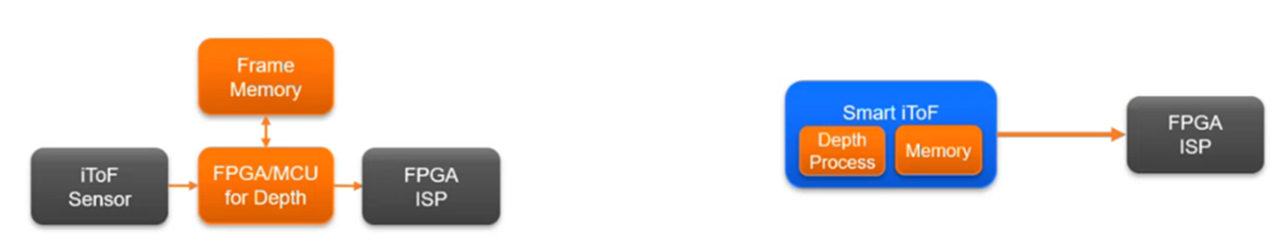
Detailing the Hyperlux ID AdvancesOnsemi’s Hyperlux ID sensing family initially consists of two 1.2 megapixels (MP) iToF products, the AF0130 and AF0131. This family provides advanced sensor performance and development in four critical areas:
- Receiving reliable depth information with moving objects
Achieving optimal resolution/depth distance with high accuracy
- Reducing cost and size
- Decreasing calibration time
Each of the aforementioned areas and improvements are further detailed.
Momentum Motion ArtifactsTo enable more widespread adoption, iToF sensors need to function well with moving objects, so they can produce accurate results without motion. As mentioned, iToF sensing on light reflections using four or more different phases to calculate depth. Nearly all existing iToF sensing solutions in the marketplace do not capture and process these phases simultaneously provide which issues with moving objects. Designed with a unique proprietary integration and readout structure, the Hyperlux ID depth sensor uses global shutter with on-chip storage and real-time processing to enable fast-moving object capture applications such as conveyor belt operation, robot arms, surveillance, collision collision, attachment detection and more.
 iToF Applications in Warehouse
Increased Resolution = Higher Accuracy and Expanded Depth
iToF Applications in Warehouse
Increased Resolution = Higher Accuracy and Expanded Depth
Most iToF sensors on the market today have only VGA resolution, which hinders their accuracy, and in turn, limits their applications. One reason VGA is more prevalent is due to the complex phase capture and data intensive processing mentioned prior. In contrast, the Hyperlux ID sensors are designed with 1.2 MP resolution (1280×960) using a high performance 3.5 μm back-side (BSI) pixel. As a product of its increased resolution over VGA, the Hyperlux ID sensor offers the additional critical advantage of expanded range depth. , at closer distances high-precision accuracy is provided and wider-angle optics can be used.
With higher resolution, the Hyperlux ID sensors also deliver improved quantum efficiency and reduced depth jitter. Taken together, these enhancements mean new applications for iToF sensors where high resolution and expanded depth are paramount, such as gesture recognition, quality control/inspection and access control.
 Existing iToF solutions (left) vs onsemi’s new advanced Hyperlux ID iToF (right)
Longer Range
Existing iToF solutions (left) vs onsemi’s new advanced Hyperlux ID iToF (right)
Longer Range
As a product of increased resolution, the Hyperlux ID depth sensor can measure depth over a much greater range compared to other iToF sensors currently available. While current iToF offerings have an indoor range of less than 10 meters, the Hyperlux ID iToF sensor family can reach up to 30 meters. The usage of a high-performance global shutter pixel enables a full sensor array to closely align to active infrared lighting, which in turn limits noise provides from other infrared sources which are common indoor lights and most challenging of all – the sun.
Easier Calibration and DevelopmentAccurately record and calculating phase differences in iToF sensors require precise calibration, an extremely time-consuming process. To ease this, we have developed a proprietary method that makes Hyperlux ID sensors easier to calibrate and thus faster to set up.
To aid in development, onsemi has constructed an easy-to-use development kit that includes a baseboard, a head sensorboard and a laser board. The kit can be used both indoors and outdoors with a range of 0.5 – 30 meters. It can produce depth maps, 3D point clouds, phase-out and depth-out data from an image.
Activated, by using spread-spectrum techniques many iToF (and other infrared-enabled devices) sensors can be used in the same system without worrying of other interference devices.
onsemi’s iToF Sensors Do More for LessiToF sensors are excellent at making accurate 3D depth measurements, which have won them a solid place in industrial and commercial applications. With remarkable improvements in performance and design simplification, onsemi’s Hyperlux ID depth sensors open a new world of applications for iToF sensing depth.
Compared to iToF sensors on the market today, Hyperlux ID depth sensors work more effectively with objects in motion, outdoors and at greater distances. In addition, due to their novel design, Hyperlux ID depth sensors are more cost-effective, take up less board real estate and are easier to work with.
The Hyperlux ID family of depth sensors consists of two products: the AF0130 and AF0131. The AF0130 includes built-in depth processing while the AF0131 does not, for customers who prefer to use their own original algorithms.
The post Acquire the Current Challenges of Indirect Time-of-Flight (iToF) Technology with Technological Advancements appeared first on ELE Times.
Comptek launches Kontrox LASE 16 for industrial-scale edge-emitting laser facet passivation
Empower industrial IoT through integrated connectivity, precise positioning and value-added services with a new modem lineup from Qualcomm
Three new modems, purpose-built for IoT, bring an industry-first iSIM, cloud services and connectivity on NB-IoT and Cat 1bis networks for ubiquitous coverage.
The industrial Internet of Things (IIoT) is rapidly transforming industries, enabling businesses to achieve greater efficiency, productivity and visibility. However, deploying successful IIoT applications requires reliable connectivity, accurate positioning and cost-effective solutions. Three new modems from Qualcomm Technologies are purpose-built to address far-ranging use cases across industrial applications through an industry-first integrated SIM (iSIM), and LTE connectivity on Narrowband IoT (NB-IoT) and Cat 1bis networks, for coverage even in challenging signal environments.
The Qualcomm E41 4G Modem-RFThe Qualcomm E41 4G Modem-RF evolves IoT device capabilities by bringing integrated connectivity through an industry-first GSMA pre-certified iSIM. It offers device manufacturers the ability to simplify the device manufacturing process by reducing the need for additional parts and multiple models of the same device, helping accelerate the time to market of commercial devices, since those devices can be remotely provisioned to the desired network once manufactured through integrated connectivity capabilities. The E41 4G Modem-RF is also purpose-built for use with the Qualcomm Aware Platform so enterprises, OEMs, ODMs and developers can easily build, deploy and scale cloud-connected devices that can be tailored to solve various industrial challenges across businesses, through value-added, cloud-based services.
The Qualcomm E51 4G Modem-RF and Qualcomm E52 4G Modem-RFContinuing the mission of advancing cellular connectivity for everyone and across every device, Qualcomm is proudly introducing a new generation of modem solutions for IoT, optimized for use on NB-IoT and Cat 1bis networks. Both the Qualcomm E51 4G Modem-RF and the Qualcomm E52 4G Modem-RF feature a highly integrated design that allows for power and cost optimizations for device manufacturers. These two low-power solutions contain an integrated power management unit, support for RF communications, and a rich array of peripherals.
The former of these two solutions also removes the need for dedicated GPS hardware through cloud-based GPS positioning services, further helping device manufacturers save on device costs, while reducing positioning error in open sky and dense urban environments. Regardless of which modem ODMs and OEMs choose, they can rest assured they can utilize low-power connectivity and intelligent power management capabilities, and NB-IoT or Cat 1bis connectivity, making these modems ideal for ultra-low power connectivity across a range of IoT devices including smart meters, smart city devices, intelligent parking solutions, healthcare devices, wearable devices, IP cameras, point-of-sale terminals and more.
 Integrated global connectivity
The Qualcomm E41 4G Modem-RF and Qualcomm E52 4G Modem-RF are both Cat 1bis solutions that represent advancements in IIoT connectivity, including a breakthrough on the former of these modems, which features an industry-first, GSMA pre-certified iSIM solution that can be programmed during manufacturing or remotely via a SIM provisioning service. This will enable devices to more readily connect to a variety of cellular networks across the globe, thereby making it easier than ever for ODMs, OEMs, MNOs and MVNOs to integrate connectivity on devices across networks.
The potential applications for the E41 4G Modem-RF span across a variety of IoT devices, including smart meters that are placed in remote areas that have historically required frequent battery replacements or manual readings. Now, those meters can operate more efficiently by using integrated connectivity and remote management to send readings proactively over the air, and alert remote decision-makers when maintenance is needed.
 Positioning in any environment
IoT devices are deployed in a variety of environments, including where location technologies have traditionally been challenged, such as indoor areas like warehouses and retail stores. The E41 4G Modem-RF uses several positioning techniques to address the needs of industrial IoT applications, including in these difficult signal environments, using ambient signals from existing Wi-Fi access points and cellular towers. Positioning can be achieved either directly through the modem, or through Qualcomm Aware Positioning Services, which adds cloud-based positioning services and available GNSS assistance, when paired with the all-new optional dual-band GNSS receiver, the Qualcomm QCG110. This is an ideal solution for positioning devices in open-sky environments that require precise positioning, using multiple constellations, in a power-conscious way.
With its variety of positioning technologies, the E41 4G Modem-RF provides a robust solution for IIoT applications including asset tracking and fleet management, energy and utilities, retail and mobile network operators, powering continuous asset visibility, monitoring and management capabilities even in the most challenging conditions.
 Cost-conscious design
All three new modems will help device manufacturers simplify the development process and reduce the time and costs to develop devices through a highly integrated design architecture. Because the E41 4G Modem-RF incorporates iSIM technology directly into the hardware design, it reduces the total cost of assembling a device, since the cost of SIM card is included in the modem. OEMs are able to develop a single device model that can be remotely programmed to work in different regions around the globe and transform the traditional manufacturing model where it’s been necessary to build multiple models of the same device, each using a different SIM, to work with different connectivity providers across regions. By utilizing the E41 4G Modem-RF’s compact design, businesses can unlock the full potential of IIoT without compromising on quality or performance, and reduce design complexity.
 Powering a variety of industrial uses
The capabilities of all three modems unlock a wide variety of possibilities across smart wearables in warehousing, industrial handheld devices in retail, smart metering in energy and utilities, guidance for autonomous robots across retail, warehouses and more.
In the energy and utilities sector, example uses for all three of these modems include:
- Improved operational efficiency and energy distribution on a localized grid level with reduced costs through less manual intervention.
- Long-lasting asset control capabilities for vital infrastructure, such as electric meters, through precise data collection and remote management capabilities.
- High temperature support allows devices to be deployed and used in harsh environments that are typical of energy and utilities space.
- IP cameras, wearable devices, smart meters and industrial handheld devices.
In the retail sector, examples of solutions the E41 4G Modem-RF can power include:
- Real-time inventory management and security-focused payment processing to point-of-sale systems and industrial handheld devices.
- On-device AI capabilities and advanced security surveillance functionality on IP cameras with real-time alerts and remote monitoring capabilities.
For autonomous robots in manufacturing, logistics and retail applications, the E41 4G Modem-RF provides:
- Precise positioning and connectivity, delivering efficient navigation and automation.
- Low-latency and security-focused processing for enhanced reliability during use.
At its core, the integrated and compact design of these three modems supports a wide range of IoT applications that demand both precise, low-power positioning and seamless connectivity, within a single, versatile design that can be selected depending on the target application, empowering businesses across multiple industries to achieve growth and seize new opportunities.
The post Empower industrial IoT through integrated connectivity, precise positioning and value-added services with a new modem lineup from Qualcomm appeared first on ELE Times.
👍 Конференція трудового колективу КПІ ім. Ігоря Сікорського

17 квітня 2025 року відбудеться конференція трудового колективу КПІ ім. Ігоря Сікорського у Центрі культури та мистецтв КПІ
Optimize power and wakeup latency in swift response vision systems – Part 2

Part 1 of this article series provided a detailed overview of a trigger-based vision system for embedded applications. It also delved into latency measurements of this swift response vision system while explaining latency-related design strategy and measurement methods. Now, Part 2 provides a detailed treatment of optimizing power consumption and wakeup latency of this embedded vision system.
In Linux, power management is a key feature that allows the system to enter various sleep states to conserve energy when the system is idle or in a low-power state. These sleep states are typically categorized into “suspend” (low-power modes) and “hibernate” (suspend to disk) modes that are part of the Advanced Configuration and Power Interface (ACPI) specification. Below are the main Linux sleep states.

Figure 1 Here is a highlight of Linux sleep states. Source: eInfochips
- Wakeup (Idle): System fully active; CPU and components fully powered, used when the device is actively in use; high power consumption, no resume time needed.
- Deep sleep (Suspend-to-RAM): CPU and motherboard components mostly disabled, RAM refreshed, used for deeper low-power states to save energy; low power consumption varying by C-state, fast resume time (milliseconds).
- System sleep (Suspend-to-Idle): CPU frozen, RAM in self-refresh mode, shallow sleep state for low-latency, responsive applications (for example, network requests); low power consumption, higher than hibernate, fast resume time (milliseconds).
- Hibernate (Suspend-to-Disk): Memory saved to disk, system powered off, used for deep power savings over long periods (for instance, laptops); almost zero power consumption, slow resume time (requires reading from disk).
Suspend To Ram (STR) offers a good balance, as it powers down most of the system but keeps RAM active (self-refresh mode) for a quick resume, making it suitable for devices needing quick wakeups and energy savings. Hibernate, on the other hand, saves more power by writing the system’s state to disk and powering down completely, but resulting in slower wakeup times.
Qualcomm’s chips, especially those found in Linux embedded devices, support two power-saving modes to help optimize battery life and improve efficiency. These power-saving modes are typically controlled through the system’s firmware, the operating system, and specific hardware components. Here are the main power-saving modes supported by Qualcomm-based chipsets:
- Suspend to RAM (STR)
- Suspend to Idle (S2Idle)
Triggers suspend mode by writing “mem” or “freeze” in /sys/power/state.

Figure 2 Here is how source flow looks like when device enters sleep and wakes up. Source: eInfochips
As the device goes into suspend modes, it performs the following tasks:
- Check whether the suspend type is valid or not
- Notify user space applications that device is going into sleep state
- Freeze the console logs
- Freeze kernel thread and buses and freeze unwalkable interrupts
- Disable non-bootable CPU (CPU 1-7) and keep RAM into self-refresh mode
- Keep the device into sleep state until any wakeup signal is received
Once the device receives the wakeup interrupt or trigger, it starts resuming the device in reverse order while suspending the device.
While the system is suspended, the current consumption of the Aikri QRB4210 system on module (SoM) comes around to ~7 mA at 3.7-V supply voltage. Below is the waveform of the current drained by the system on module.

Figure 3 Here is how current consumption looks like while Aikri QRB4210 is in suspend mode. Source: eInfochips
Camera sensor power modes
Camera sensors are designed to support multiple power modes such as:
- Streaming mode
- Suspend mode
- Standby mode
Each mode has distinct power consumption and latency. Latency varies by power-saving level and sensor state. Based on use case, ensure the camera uses the most efficient mode for its function, especially while the system is in power saving mode like deep sleep or standby. This ensures balanced performance and power efficiency while maintaining quick reactivation.
In GStreamer, the pipeline manages data flow through various processing stages. These stages align with the GStreamer state machine, marking points in the pipeline’s lifecycle. The four main states are NULL, READY, PAUSED and PLAYING, each indicating the pipeline’s status and controlling data and event flow. Here’s a breakdown of each of the stages (or states) in a GStreamer pipeline:

Figure 4 The above image outlines GStreamer’s pipeline stages. Source: eInfochips
- Null
- This is the initial state of the pipeline, and it represents an inactive or uninitialized state. The pipeline is not doing any work in this state. All elements in the pipeline are in their NULL state as well.
- In this state, the master clock (MCLK) from the processor to the camera sensor is not active; the camera sensor is in reset state and the current consumption by the camera is almost zero.
- Ready
- In this state, the pipeline is ready to be configured but has not yet started processing any media. It’s like a preparation phase before actual playback or processing starts.
- GStreamer performs sanity check and plugin compatibility for the given pipeline.
- Resources can be allocated (for example, memory buffers and device initialization).
- GStreamer entering this state does not impact MCLK’s state or reset signal. If GStreamer enters from the NULL state to the READY state, the MCLK remains inactive. On the other hand, if it enters the READY state from the PLAYING state, the MCLK remains active.
- The current consumption in the READY state depends on the previous state; this behavior can be further optimized.
- Paused
- This state indicates that the pipeline is set up and ready to process media but is not actively playing yet. It’s often used when preparing for playback or streaming while maintaining control over when processing starts.
- All elements in the pipeline are initialized and ready to start processing media.
- Like the READY state, the current consumption in the PAUSED state depends on the previous state, so some optimization in the camera stack can help reduce the power consumption during this state.
- Playing
- The PLAYING state represents the pipeline’s fully active state, where data is being processed and media is either being rendered to the screen, played back through speakers, or streamed to a remote system.
- MCLK is active and the camera sensor is out of reset. The current consumption is highest in this state as all camera sensor data is being captured and passed through the pipeline.
To minimize wakeup latency of the camera sensor while maintaining the lowest sleep current, GStreamer pipeline should be put in the NULL state when the system is suspended. To understand the power consumption due to MCLK and RESET signals assertion, below is the comparison of current consumption between the NULL state of GStreamer pipeline and the READY state of GStreamer pipeline while QRB4210 is in the suspended state.

Figure 5 Current consumption shown while GStreamer is in NULL state and QRB4210 is in suspend mode at ~7 mA. Source: eInfochips

Figure 6 Current consumption shown while GStreamer is in READY state and QRB4210 is in suspend mode at ~30 mA. Source: eInfochips
While the camera is in the NULL state, the QRB4210 system on module draws a current of ~7mA, which is equivalent to the current drawn by the system on module in the suspended state when no camera is connected. When the camera is in the READY state, the QRB4210 system on module draws a current of around ~30 mA. The above oscilloscope snapshot shows the waveforms of the consumed current. All the measured currents are at 3.7-V supply voltage for the QRB4210 system on module.
Latency measurement results
Latency was measured between two trigger events: the first occurs when the device wakes up and receives the interrupt at the application processor, and the second occurs when the first frame becomes available in the DDR after image signal processor (ISP) runs.
As mentioned earlier in Part 1, the scenario is simulated using bash script that keeps the device into the suspend mode and triggers the QRB4210 platform from sleep and wakeup using the RTC wake alarm.
We have collected the camera wakeup latency by changing the camera state from PLAYING to READY and from PLAYING to NULL. In each scenario, three different use cases are followed, which are recording camera stream into eMMC, recording camera stream into SD card, and previewing camera stream to display. The resulting latency is as follows:
- Camera state in READY

Table 1 Latency measurements are shown in READY state. Source: eInfochips
- Camera state in NULL

Table 2 Latency measurements are shown in NULL state. Source: eInfochips
The minimum, maximum, and average values presented in the above tables have been derived by running each scenario for 100 iterations.
Apart from measuring the latency numbers programmatically, below are the results measured using the GPIO toggle operation between two reference events while switching the camera state from READY to PLAYING.

Table 3 Latency measurements are conducted using GPIO. Source: eInfochips
Now refer to the following oscilloscope images for different scenarios used in the GPIO toggle measurement method.

Figure 7 GPIO toggle measurements are conducted while recording into eMMC at 410.641 ms. Source: eInfochips

Figure 8 GPIO toggle measurements are conducted while recording into SD card at 382.037 ms. Source: eInfochips

Figure 9 GPIO toggle measurements are conducted during preview on display at 359.153 ms. Source: eInfochips
Trade-off between current consumption and wakeup latency
Based on the simulated result, we see that current consumption and wakeup latency are dependent on each other.
The consolidated readings show that a camera pipeline in the READY state consumes more current while it takes less time to wake up. On the other hand, if the camera pipeline is in the NULL state, it consumes less current but takes more time to wake up. Refer to the table below for average data readings.

Table 4 The above data shows trade-off between current consumption and wakeup latency. Source: eInfochips
All latency data is measured between the reception of the wakeup IRQ at the application processor and the availability of the frame in DDR after the wakeup. It does not include the time taken by a motion detection sensor to sense and generate an interrupt for the application processor. Generally, the time taken by a motion detection sensor is negligible compared to the numbers mentioned above.
Future scope
To reduce the current consumption of a device in the sleep state optimization, you can follow the steps below:
- Disable redundant peripherals and I/O ports.
- Prevent avoidable wakeups by ensuring that peripherals don’t resume from sleep unnecessarily.
- Disable or mask unwanted wakeup triggers or subsystem that can wake the device from a sleep state.
- Use camera standby (register retaining) mode so that MCLK can be stopped, or its frequency can be reduced.
- Enable LCD display only when preview use case is running.
To optimize wakeup latency, follow the guidelines below:
- Make use of the camera standby mode to further optimize latency to generate the first frame.
- Reduce camera sensor frame size to optimize frame scan time and ISP processing time.
- Disable redundant system services.
- Trigger camera captures from lower-level interface rather than using the GStreamer.
Trigger-based cameras offer an efficient solution for capturing targeted events, reducing unnecessary operation, and managing resources effectively. They are a powerful tool in applications where specific, event-driven image or video capture is needed.
By conducting experiments on the Aikri QRB4210 platform and making minimal optimizations to the Linux operating system, it’s possible to replicate or create a robust trigger-based camera system, achieving ~400-500 ms latency with minimal current consumption.
Jigar Pandya—a solution engineer at eInfochips, an Arrow company—specializes in board bring-up, board support package porting, and optimization.
Priyank Modi—a hardware design engineer at eInfochips, an Arrow company—has worked on various Aikri projects to enhance technical capabilities.
Related content
- The State of Machine Vision
- What Is Machine Vision All About?
- Processors, Sensors Drive Embedded Vision
- Shaping the Scene for Vision Standardization
- Embedded Vision: Giving Machines the Power of Sight
The post Optimize power and wakeup latency in swift response vision systems – Part 2 appeared first on EDN.
Виконання бюджету за 2024 рік

Надходження до бюджету університету за 2024 рік перевищили відповідний показник минулого року на 12,5 % і склали 2 450,6 млн грн.
The (more) modern drone: Which one(s) do I now own?

Last September, I detailed why I’d decided to hold onto the first-gen DJI Mavic Air drone that I’d bought back in mid-2021 (and DJI had introduced in January 2018), a decision which then prompted me to both resurrect its long-drained batteries and acquire a Remote ID module to get it copacetic with current FAA usage regulations, as subsequently mentioned in October:

Within both blog posts, however, I intentionally alluded to (but didn’t delve into detail on) the newer drone that I’d also purchased to accompany it, aside from dropping hints that it offered (sneak peek: as-needed enabled) integrated Remote ID support and weighed (sneak peek: sometimes) less than 250 grams. That teasing wasn’t (just) to drive you nuts: to do the topic justice would necessitate a blog post all its own. That time is now, and that blog post is this one.
Behold DJI’s Mini 3 Pro, originally introduced in May 2022 and shown here with its baseline RC-N1 controller:

I bought mine (two of them, actually, as it turned out) roughly two years post-intro, in late June (from eBay) and early July (from Lensrentals) of last year. By that time, the Mini 4 Pro successor, unveiled in September 2023, had already been out for nearly a year. So, why did I pick its predecessor? The two drone generations look identical; they take the same batteries, propellers and other parts, and fit into the same cases. And as far as image capture goes, the sensors are identical as well: 48 Mpixel (effective) 1/1.3″ CMOS.
What’s connected to the image sensors, however, leads to one of several key differences between the two generations. The Mini 3 Pro captures video at up to 4K resolution at a 60-fps peak frame rate. The improved ISP (image signal processor) in the Mini 4 Pro, conversely, also captures video at 4K resolution, but this time up to a 100-fps frame rate. Dim-light image quality is also improved, along with the available capture-format options, now also encompassing both pre-processed HDR and post-processed D-LOG. And the camera now rotates a full 90° vertical for TikTok- and more general smartphone viewing-friendly portrait orientation video frames.
Speaking of cameras, what about the two drones’ collision avoidance systems? The DJI Mini 3 Pro has cameras both front and rear for collision avoidance purposes, along with another pointing downward to (for example) aid in landing. The Mini 4 Pro replaces them with four fisheye-lens cameras (at front, rear and both sides) for collision avoidance all around the drone as well as above it, further augmented by two downward facing cameras for stereo distance and a LiDAR sensor, the latter enhancing after-dark sensing and discerning distance-to-ground when the terrain is featureless. By the way, the rumored upcoming DJI Mini 5 Pro further bolsters the drone’s LiDAR facilities, if the leaked images are true and not just Photoshop-created fakes.
The final notable difference involves the contrasting wireless protocols used by both drones to communicate with and stream live video to the user’s controller and, if used, goggles. The Mini 3 Pro leverages DJI’s O3 transmission system, with an estimated range of 12 km while streaming live 1080p 30 fps video. With the Mini 4 Pro and its more advanced O4 system, conversely, the wirelessly connected range increases to an estimated 20 km. Two important notes here:
- The controllers for the Mini 3 Pro also support the longer-range (15 km) and higher frame rate (1080p 60 fps) O3+ protocol used by larger DJI drones such as the Mavic 3
- Unfortunately, however, the DJI Mini 4 is not backwards compatible with the O3 and O3+ protocols, so although I’ll be able to reuse my batteries and the like if I do a drone-generation upgrade in the future, I’ll need to purchase new controllers and goggles for it.
That all said, why did I still go with the Mini 3 Pro? The core reason was cost. In assessing the available inventory of used drone equipment, the bulk of the options I found were at both ends of the spectrum: either in like-new condition, or egregiously damaged by past accidents. But given that the Mini 3 Pro had been in the market nearly 1.5 years longer, its available used inventory was much more sizeable. I was able to find two pristine Mini 3 Pro examples for a combined price tag less than that of a single like-new (far from brand new) Mini 4 Pro. And the money saved also afforded me the ability to purchase two used upgraded integrated-display controllers, the mainstream RC and high-end RC Pro, the latter running full-blown Android.


Although enhancements such as higher quality video, more advanced object detection and longer range are nice, they’re not essential in my currently elementary use case, particularly counterbalanced against the fiscal savings I obtained by going prior-gen. The DJI Mini 4’s expanded-scope collision avoidance might be useful when flying the drone side-to-side for panning purposes, for example, or through a grove of trees, neither of which I see myself doing much if any of, at least for a while. And considering that after 12 km the drone will probably already be out of sight, combined with the alternative ability to record even higher quality video to local drone microSD storage, O4 transmission system support also isn’t a necessity for me.
Speaking of batteries (plenty of spares which I now also own, along with associated chargers, and refresh-charge them every two months to keep them viable) and range, let’s get to the drone’s earlier-alluded Remote ID facilities. The Mini 3 Pro (therefore also Mini 4 Pro) has two battery options: a standard 2453 mAh model that, as conveniently stamped right on it to answer enforcement agency inquiries, keeps the drone just below the 250-gram threshold:

and a “Plus” 3850 mAh model that weighs ~50% more (121 grams vs 80.5 grams). The DJI Mini 3 Pro has built-in Remote ID support, negating the need for an add-on module (which, if installed, would push total weight above 249 grams, even using a standard battery). But here’s the slick bit; when the drone detects that a standard battery is in use, it disables Remote ID transmission, both because the FAA doesn’t require it and to address user privacy concerns, given that scanning facilities are available to the masses, not just to regulatory and enforcement entities.
I’ve admittedly been too busy post-purchase to use the drone gear much yet, but I’m looking forward to harassing the neighbors  (kidding!) with it in the future. I’ve also acquired a Goggles Integra set and a RC Motion 2 Controller, both gently used from Lensrentals:


to test out FPV (first-person view) flying, and even a LTE cellular dongle for remote-locale Internet access to the RC Pro controller (unfortunately, such dongles reportedly can’t also be used on the drone itself, at least in the US, for alternative long-range controller connectivity):

And finally, I’ve acquired used examples of the Googles Racing Edition Set (Adorama) and OcuSync Air System (eBay) for the Mavic Air, again for FPV testing purposes:


Stay tuned for more on all of this if (hopefully more accurately, when) I get time to actualize my drone gear testing aspirations. Until then, let me know your thoughts in the comments!
—Brian Dipert is the Editor-in-Chief of the Edge AI and Vision Alliance, and a Senior Analyst at BDTI and Editor-in-Chief of InsideDSP, the company’s online newsletter.
Related Content
- Diagnosing and resuscitating a set of DJI drone batteries
- Teardown: DJI Spark drone
- Oh little drone, how you have grown…
- Drone regulation and electronic augmentation
- Keep your drone flying high with the right circuit protection design
The post The (more) modern drone: Which one(s) do I now own? appeared first on EDN.
Кампанію декларування за 2024 рік завершено

Цьогоріч свої декларації подали майже 627 тисяч осіб, які виконують функції держави або місцевого самоврядування. Це важливий показник, адже, попри всі виклики, значна кількість посадовців вкотре підтвердила готовність діяти відкрито й прозоро.
[проєкт] Колективний договiр Національного технічного університету України «Київський політехнічний інститут імені Ігоря Сікорського» на період з квітня 2025 р. по квітень 2030 р.
Колективний договір укладено відповідно до чинного законодавства, у тому числі з дотриманням Законів України "Про колективні договори і угоди", "Про освіту", "Про вищу освіту", "Про оплату праці", "Про охорону праці", "Про відпустки", "Про професійні спілки, їх права та гарантії діяльності", КЗпП України, Генеральної і Галузевої угод та ін.
PhotonDelta and Silicon Catalyst collaborate to drive innovation for early-stage photonic startups
Optical inspection system for a complete 3D sintering paste check
Future-proof quality assurance for power electronics through sintering paste inspection with multi-line SPI
Higher operating temperatures, thinner interconnection layers, 10 times the longevity – the advantages of sintering pastes over solder pastes have long been recognized in the field of power electronics. Not least for this reason, sintering pastes are preferred in system-critical technologies such as “green energy” and e-mobility. Here, for example, IGBTs have become the central component in converters for all types of electric drives: wind turbines, solar power generation, battery charging – hardly any future technology would be conceivable without the “all-rounder” sintering paste. However, sintering is more prone to errors than soldering paste printing. Furthermore, defects are more difficult to detect and rectify – critical failures in the field are the result. To avoid this, GÖPEL electronic has now added an inspection system specifically for sintering paste to its Multi Line platform.
The Multi Line SPI is a cost-effective 3D inline system for automated inspection of sintering paste. Based on the Multi Line platform, it is a customized solution for small and medium-sized companies with high quality standards; it can also be used for solder pastes. The telecentric 3D camera module is used to inspect solder and sinter paste without shadows for shape, area, coplanarity, height, bridges, volume and X/Y offset. Equipped with two digital fringe projectors for shadow-free 3D image capturing, it has a resolution of 15µm/pixel, a height measurement accuracy of 1µm and a height resolution of 0.2 µm. This means that measurement values can be obtained precisely and repeatedly.
Generation of an inspection program for sinter paste inspection takes only a few minutes: CAD data or a reference layout is sufficient. Users who already use GÖPEL electronic software for programming SMD, THT or CCI systems can learn the additional sinter paste functions with little training. In addition, the data import, verification and statistics software are identical to the other inspection systems from GÖPEL electronic. This is where the platform concept of the Multi Line series really pays off: the uniform, powerful operating and evaluation software across all devices reduces training and programming effort, enabling flexible and optimized staff deployment planning.
The post Optical inspection system for a complete 3D sintering paste check appeared first on ELE Times.
Keysight and SAMEER Collaborate to Advance 6G and Healthcare Innovation in India
- Collaboration brings together expertise and cutting-edge technology to drive innovation
- Provides essential 6G research infrastructure to bolster the ‘Made in India’ vision
Keysight Technologies, Inc. announces it has signed a Memorandum of Understanding with Society for Applied Microwave Electronics Engineering & Research, a premier R&D organisation under Ministry of Electronics and Information Technology, Government of India to drive healthcare and 6G innovation across India. As part of the collaboration, both Keysight and SAMEER have proposed to create a healthcare center of excellence along with a research lab to drive 6G communication research.
In order to scale-up the Indian presence in 6G and other critical areas such as medical electronics, there is an urgent need to build strong expertise and an ecosystem in India. Keysight and SAMEER, which is part of the government research institute under the Ministry of Electronics & Information Technology will work together to address this. Building on existing work, the collaboration will focus on several key technology areas to meet the growing demand for innovation in both the strategic and civilian applications.
Under the MoU, Keysight will enable SAMEER to develop and demonstrate fully functional labs that support 6G research and development across various India institutions. Plans also include establishing a center of excellence for healthcare focused on advancing magnetic resonance imaging (MRI) technologies. Together, the two organizations will work on driving innovation and supporting the ‘Made in India’ initiative which is designed to generate local growth and development.
Dr P.Hanumantha Rao, Director General at SAMEER said: “We are leading 6G research in India after the successful demonstration of our end to end 5G stack along with IIT Madras. The proposed collaboration with Keysight will enhance this further and enable Indian research and academic institutions to get access to next generation technologies.”
SAMEER contributions in healthcare include fully indigenous Linear Accelerator for Cancer therapy and a fully functional affordable 1.5T MRI. The MoU will facilitate Keysight to leverage the products developed by SAMEER for democratization across India and continue research by complementing each other’s capabilities.
Sudhir Tangri, Vice President of Asia Pacific Sales and Country General Manager of India at Keysight said: “Establishing a center of excellence and building 6G research areas is a critical step towards driving innovation in India. Through this collaboration we are proud to provide the much-needed infrastructure and technology that will empower future research across healthcare and other sectors. SAMEER is a leader in its field, and we are excited to work together to accelerate our 6G and healthcare vision.”
The post Keysight and SAMEER Collaborate to Advance 6G and Healthcare Innovation in India appeared first on ELE Times.
Сторінки


![[link]](https://i.redd.it/4d398m5q0mte1.jpeg)