
Збирач потоків
The Hardware Book (the largest reference for connector pinouts, cables, adapters, and technical specifications) is back online
Проректорка Тетяна Желяскова: "У ДНК КПІ – інноваційність і командна робота"

Комфортний клімат у службовому кабінеті проректорки з навчальної роботи Національного технічного університету України "Київський політехнічний інститут імені Ігоря Сікорського" Тетяни Желяскової відчувається відразу. Світле приміщення, зручне крісло біля масивного глянцевого столу, де є місце для безлічі документів, книг, ділових паперів. На підвіконні в ідеальному порядку горщики з вишуканими білими орхідеями. У цьому кабінеті Тетяна Миколаївна не лише працює сама, але й спілкується з колегами, і таке живе спілкування, за її словами, вона дуже цінує. Але березень, що буяє за вікном, налаштовує спочатку на не зовсім дотичне до професійних обов'язків проректорки запитання.
How Ethernet accelerates the move to software-defined vehicles
By: Madison Ecklund, systems manager, Body Electronics & Lighting
A zone architecture and Ethernet represent the future of networking in vehicles. New features in vehicles, as well as the shift to aggregating sensors and actuators into zonal control modules, require a high-bandwidth and low-latency in-vehicle communication network. A zone architecture implementing Ethernet enables the growing trend of the software-defined vehicle.
Most vehicles today are built using a type of wiring and electronic control unit (ECU) architecture called a domain architecture. A domain architecture categorises ECUs into domains based on specific functions, regardless of their physical location in the vehicle.
A zone architecture, in contrast to a domain architecture, organises communication, power distribution and load control by location rather than by function, as shown in Figure 1. A zonal control module behaves as a network data bridge between the vehicle’s computing system and local edge nodes such as smart sensors and ECUs. To reduce cabling in the vehicle, a zonal control module will also distribute power to different edge nodes (by implementing semiconductor smart fuse capabilities), handle low-level computing, and drive local loads such as motors and lighting.
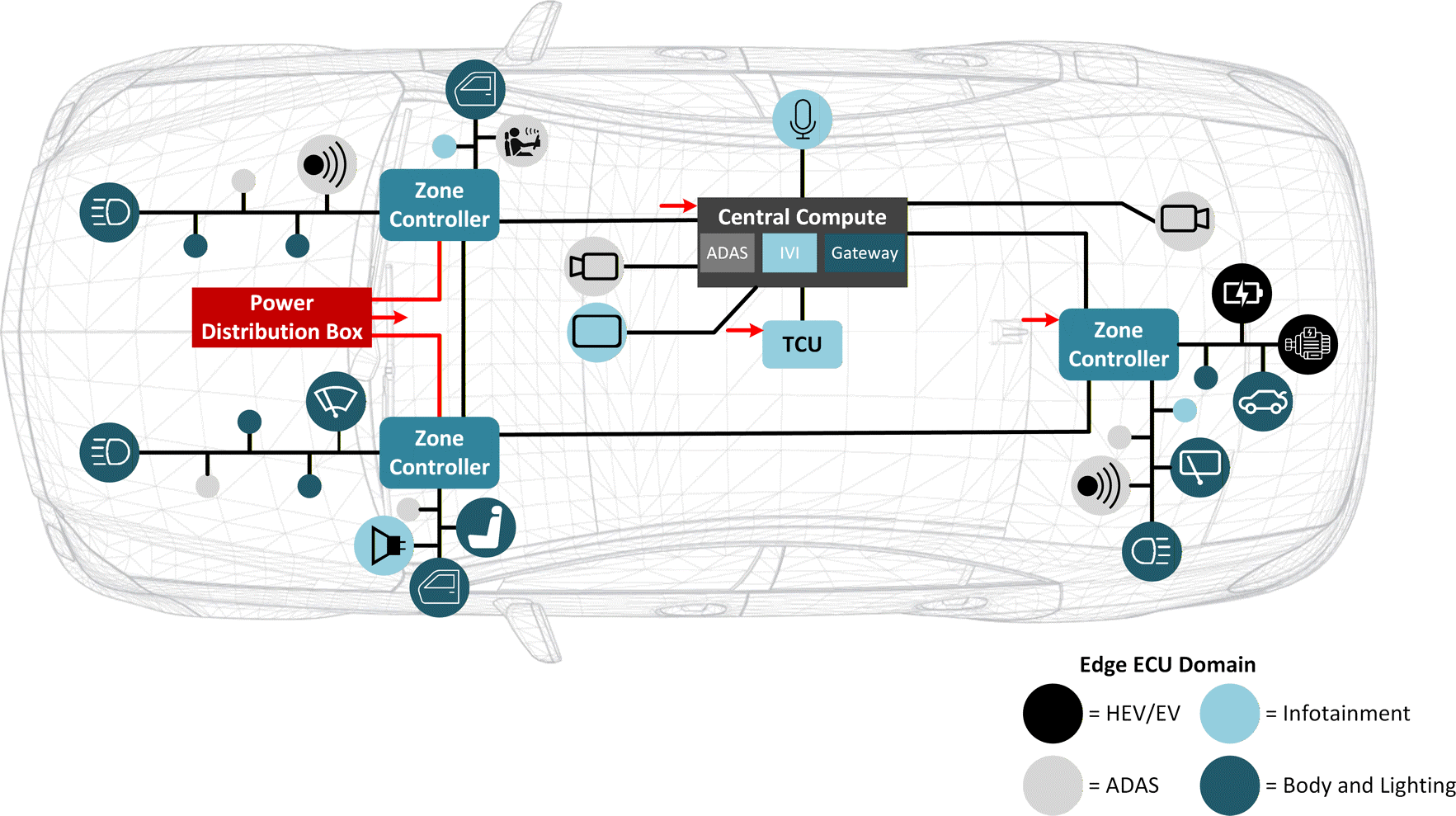 Figure 1. Example of a zone architecture
Zonal control modules transfer data from various sensors and ECUs through an edge-node communication network and forward the combined sensor data to the central computing system through backbone communication. Similarly, the zonal control modules transfer data received from the central computing system to various actuators, again through backbone communication, and again through an edge-node communication network. This two-way communication between the central computing system and the zonal control modules requires a high-bandwidth and low-latency communication backbone in order to handle the large amount of data generated by functions such as multiple advanced driver assistance system (ADAS) sensors, vehicle motion control and adaptive driving beams.
Bandwidth requirements in a zone architectureTo understand the value in using Ethernet in vehicles, let’s break down Ethernet use by application. The newly defined Single-Pair Ethernet supports speeds from 10Mbps to 10Gbps, defined through Institute of Electrical and Electronics Engineers (IEEE) 802.3cg (10Mbps), IEEE 802.3bw (100 Mbps), IEEE 802.bu (1Gbps) and IEEE 802.3ch (10Gbps). All of these new Ethernet technologies work over a single-pair cable and can communicate at distances as far as 15m, which is long enough to cover the longest link in a vehicle. Ethernet can also enable the time synchronisation of sensor data using IEEE 802.1AS timestamping to achieve low latency.
While Ethernet is capable of extremely fast speeds, these speeds are not necessary in every context. For example, communicating with the door control module or the heating, ventilation and air-conditioning system does not require a 100Mbps data rate. A 10Mbps Ethernet PHY, such as the DP83TD555J-Q1, or an alternative network protocol, such as Controller Area Network (CAN), is better for lower-speed and less bandwidth-intensive use cases, while reserving higher speeds for sending aggregated camera and autonomous driving sensor data from the zonal control modules to the central computing system. Figure 2 shows where to use different speeds of Ethernet in a zone architecture.
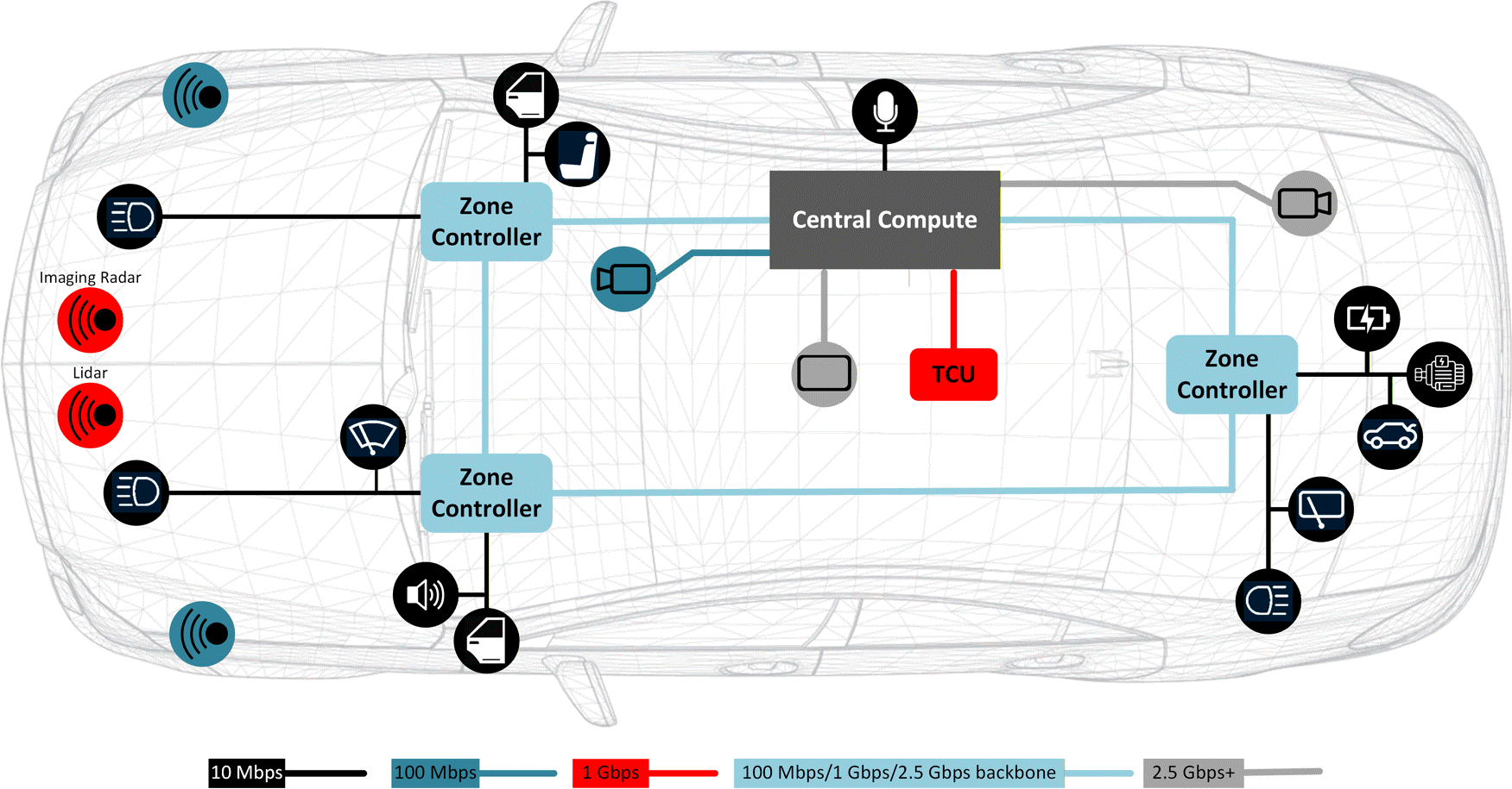 Figure 2. Ethernet in a zone architecture
Using Figure 2, let’s take a closer look at the communication speeds used for radar, lidar, camera and body applications. When the radar or lidar system-on-a-chip (SoC) processes the data, typically CAN, 10Mbps Ethernet or 100Mbps Ethernet communicates lidar or radar data to the zonal control module. When only first- or second-level data processing occurs, 100Mbps to 1Gbps Ethernet communicates radar and lidar data to the zonal module or central computer. Sending raw lidar or radar data to the central computing system for processing will extract more information through sensor fusion of various sensors. The transmission of such a large amount of raw data requires a higher bandwidth, typically a serial/deserializer (SerDes) protocol or 2.5Gbps plus Ethernet.
For cameras, SerDes such as Flat Panel Display (FPD)-Link is the most appropriate protocol when a level of increased ADAS data requires all of the raw data from the front camera for post-processing.
If it is possible to compress the data from the front camera and you don’t need this increased level of ADAS data, 100Mbps Ethernet is an alternative.
Body domain modules such as door handle sensors, window-lift control modules and side mirror control modules traditionally use the CAN and Local Interconnect Network (LIN) protocols to communicate, as neither requires a high bandwidth. While designers will continue to use CAN and LIN, the increased use of Ethernet in vehicles also creates a place for 10Mbps 10BASE-T1S multidrop Ethernet. Ethernet is traditionally a point-to-point topology, but 10BASE-T1S Ethernet is the first Ethernet standard enabling functionality over a bus topology.
Multigigabit Ethernet in a zone architectureWhat is the potential evolution of the zone architecture? It begins with aggregating body domain data, incorporating power distribution, and centralising computing. Over time, zone architectures will start aggregating data from other domains such as ADAS and infotainment. The end goal is to incorporate all domains into
the zone architecture. Regardless of which domain the data belongs to, the zonal control module and central computing system will still use the same backbone communication network to transfer data. Audio is a prime target to move into zone control modules, since it’s possible to transmit audio data over Ethernet with Audio Video Bridging standards.
Body domain functions typically require 10Mbps or less. But as ADAS or in-vehicle infotainment functions such as radar, lidar, audio and cameras become incorporated into the zone architecture, the speed and bandwidth requirements must increase and/or the Ethernet backbone topology may change from star to ring to accommodate the amount of safety-critical and time-sensitive sensor data.
Audio generates about 1.5Mbps per channel; a radar sensor typically generates 0.1Mbps to 15Mbps. Lidar generates 20Mbps to 100Mbps. Cameras generate the most 500Mbps to 3.5Gbps. Today’s vehicles typically have four to six radar sensors, one to five lidar sensors, 12 to 20 audio speakers, 12 to 16 audio microphones and six to 12 cameras. Table 1 shows the range of data generated by each type.
Table 1. Data generated in a zone architecture| Type | Data Generated | Quantity of Sensors | Low | Mid | High |
| Audio speaker | 1.5Mbps | 12 to 20 | 3.2Mbps | 24Mbps | 30Mbps |
| Audio microphone | 1.5Mbps | 12 to 16 | 3.2Mbps | 21Mbps | 24Mbps |
| Radar | 0.1 – 15Mbps | 4 to 6 | 0.4Mbps | 35Mbps | 90Mbps |
| Lidar | 20 – 100Mbps | 1 to 5 | 20Mbps | 100Mbps | 500Mbps |
| Camera | 500Mbps – 3.5Gbps | 6 to 12 | 3Gbps | 9Gbps | 42Gbps |
It is the total data being generated that is causing the push for 2.5Gbps, 5Gbps and 10Gbps Ethernet among original equipment manufacturers (OEMs). The zone architecture needs a backbone communication network capable of transmitting the enormous amount of data produced by ADAS sensors to the central computing system. Uncompressed camera data already goes beyond current Ethernet capabilities, and cameras continue increasing in resolution and pixel count. As vehicles continue toward autonomy, the number of sensors
will increase. Thus, the bandwidth required to support increased camera resolution and sensors will grow correspondingly.
The Ethernet speeds that OEMs are requesting most likely differ because of the transition schedules for incorporating different functions into the zonal control module. Audio playback on interior speakers is one of the first cross-domain data types adopted for use on the Ethernet backbone. This is likely caused by lower data generation in comparison, since 20 audio speaker channels generate about 30 Mbps. An existing 100Mbps or 1Gbps Ethernet backbone can easily accommodate the addition of audio playback data. Overall, the more high-level data functions in zonal control modules, the higher the bandwidth requirements.
Using Ethernet as the backbone for a zone architecture allows vehicles to transfer more data over the in-vehicle network when connecting to the internet or remote OEM servers. This enables subscription-based services and vehicle diagnostics through remotely performed firmware-over-the-air (FOTA) updates. FOTA updates allow for different hardware and software update cycles, which can be asynchronous as a result of the independence of sensors and actuators from the central computing node. A FOTA update can also push additional features and safety improvements, instead of waiting for a new model or having to bring the vehicle in to be worked on. Both the OEM and the customer benefit, as the OEM has control over updating the vehicle with additional features after launch, and the consumer is less inconvenienced by trips to a dealer to update firmware.
PHYs in a zone architectureEthernet requires the use of PHYs to transmit and receive high-speed data. Automotive Ethernet PHYs eliminate many of the concerns with Ethernet as the backbone of the wiring in vehicles, such as poor signal quality in
such a volatile environment. Ethernet PHYs from Texas Instruments (TI) are capable of operating at a range of temperatures from –40°C to 125°C, in compliance with Automotive Electronics Council-Q100 Grade 1 standards.
Ethernet PHYs also have to pass Ethernet compliance standards, ensuring that they meet certain interoperability and reliability standards regarding electromagnetic compatibility and electromagnetic interference, as well as IEEE conformance as specified by Open Alliance TC1 and TC12 standards, to work in a vehicular environment. With advanced diagnostic features such as signal quality indication, time domain reflectometry and electrostatic discharge sensors, PHYs are capable of detecting when errors occur and can identify these faults and enable the host system to respond proactively. For example, in the event of electrostatic discharge (ESD), the PHY sends an interrupt signal to the SoC and Media Access Control to alert it of the event and then checks other parts in the system.
Ethernet PHYs can also wake up remote ECUs over the Single-Pair Ethernet cable using the Open Alliance TC10 specification’s wake and sleep technology, which eliminates the need for a separate wire to wake
the ECUs from sleep. IEEE 802.1AE Media Access Control Security (MACsec) could also be an important technology to enable the authentication of networking ECUs and to encrypt/decrypt data to avoid cyberattacks, as cyberattacks represent the biggest threat to automotive networking.
Additional Ethernet PHYs include:
- TI’s DP83TC812-Q1, DP83TC815-Q1, and DP83TC814-Q1 100BASE-T1 PHYs have next-generation features suitable for luxury vehicles, while the smaller DP83TC813-Q1 100BASE-T1 PHY may be appealing in situations where printed circuit board space is at a premium. The DP83TG720-Q1 and DP83TG721-Q1 can connect zonal modules to data-intensive features such as the central computing system and telematics control unit, leaving headroom for the inclusion of additional features in later models without making intensive changes to the wiring harness. Combined, these PHYs open the door for more advanced and capable vehicles on the road.
- TI’s portfolio of Single-Pair Ethernet PHYs is designed to be footprint or pin-to-pin-compatible with both TI’s 100BASE-T1 and 1000BASE-T1. A single board design enables upgrades to the feature set or
bandwidth in future developments with no hardware changes. This approach helps accelerate development cycles, meet the requirements of different OEMs, and reduce time to market, thus saving R&D costs.
- The DP83TD555J-Q1 10BASE-T1S Serial Peripheral Interface MAC PHY integrates seamlessly into existing Ethernet backbone networks, eliminating protocol conversion gateways and their associated latency and processing overhead when connecting traditional CAN/LIN edge nodes. Supporting Power over Data Line, the device delivers both power and 10Mbps data over a single twisted-pair cable, reducing cable weight and system cost. Built-in PHY Collision Avoidance provides deterministic scheduling with guaranteed transmit opportunities for each network node, ensuring predictable communication timing. The larger Ethernet frame payloads enable extraction of higher data volumes and more diverse data types from ECUs at the vehicle’s edge, facilitating advanced diagnostics and over-the-air updates while maintaining real-time performance.
Advancements in automotive Ethernet technology will enable automakers to deliver more features and capabilities to new vehicles. A zone architecture implementing Ethernet will help accelerate the shift to software- defined vehicles by providing the data capacity that will support the next wave of autonomous features – leading to safer and smarter vehicles on the road.
The post How Ethernet accelerates the move to software-defined vehicles appeared first on ELE Times.
From gap to signal: Non-contact capacitive displacement sensors

Capacitive displacement sensors turn tiny gaps into actionable signals. By measuring changes in capacitance as target moves, these devices deliver precise, non-contact readings of position and motion. Their touch-free nature makes them ideal for fragile surfaces, high-speed machinery, and environments where mechanical wear is unacceptable.
From tuning dials to nanometers: The capacitive lineage
Historically, the lineage from the vintage “gang condenser” to modern capacitive displacement sensors is surprisingly direct. In early radio receivers, variable air capacitors translated a knob twist into resonance tuning by modulating plate overlap. Modern sensors exploit this same fundamental relationship—geometry and permittivity—but invert the objective.
Rather than adjusting capacitance to achieve resonance, they elevate infinitesimal ∆C into the measurement itself, quantifying motion with great fidelity. What was once a utility for frequency selection has become the primary metric of precision measurement, a century-old tuning trick reborn as precision instrumentation.

Figure 1 Rotating plates in a gang condenser modulated capacitance to tune resonance in early radio receivers. Source: Author
Capacitive sensing in everyday tools
A familiar example of this principle at work is the digital caliper. Most mainstream models utilize capacitive linear encoding: as the sliding jaw moves across a scale patterned with fixed conductive tracks, the shifting electrode geometry produces periodic variations in capacitance. The caliper’s onboard electronics digitize these differential phase shifts, translating them into precise position readouts with resolutions typically reaching 0.01 mm.
This method effectively mitigates errors from minor gaps in the slider’s fit. In essence, the tool leverages the same fundamental physics as the gang condenser—the interplay of electrode overlap and dielectric spacing—but adapts that variable capacitance into a robust, high-resolution incremental measurement system.

Figure 2 A teardown reveals the underlying sensing mechanism of a digital caliper. Source: Author
Capacitive displacement: The secret to frictionless precision
When mechanical gears grow too bulky and optical sensors prove too fragile, capacitive displacement sensing steps in. By detecting subtle shifts in an electric field—changes invisible to the eye—these sensors achieve fine accuracy. From high-end CNC machines to scientific instruments, they raise the bar for measurement—precision delivered without the drag of friction.
Capacitive displacement sensors are high-precision, non-contact instruments that measure position or distance by detecting changes in electrical capacitance. The system functions as a parallel plate capacitor, where the sensor probe serves as one conductive plate and the target object acts as the other.
As the gap (dielectric space) between the probe and the target fluctuates, the capacitance shifts in inverse proportion to the distance. By monitoring these minute variations, the sensor provides exceptionally accurate, sub-nanometer resolution measurements without ever making physical contact with the target.
In real-world practice, a capacitive displacement sensor system is not just a single probe but a complete measurement chain that typically includes a sensor head, a controller, a power supply, and cabling. The sensor head (probe) is the capacitive element that interacts with the target surface, while the controller provides excitation, interprets the capacitance changes, and outputs a usable displacement signal.
A power supply—either integrated into the controller or external—ensures stable operation, and shielded cables and connectors maintain signal integrity. For example, systems like the Lion Precision CPL series or Micro-Epsilon capaNCDT sensors use this modular setup: a probe head for sensing, a controller for signal processing, and a power supply to stabilize the system. Some controllers are designed for a single probe input, while others can accommodate multiple probes, enabling multi-point measurements when required.

Figure 3 This capacitive displacement sensor delivers single-channel, noncontact measurement for precision position and displacement applications. Source: Lion Precision
Guard ring and active guarding: Ensuring measurement integrity
On paper, the principle of capacitive displacement measurement relies on the operation of an ideal parallel-plate capacitor. When the distance between the sensor and the measurement object changes, the total capacitance varies accordingly.
If an alternating current of constant frequency and amplitude flows through the sensor capacitor, the resulting alternating voltage becomes directly proportional to the distance to the target (or ground electrode). This variation in distance is detected and processed by the controller, which then outputs a value representing the measured displacement through its designated channels.
However, since the sensor (sensing element) acts as one conductive plate and the target object as the other, accurate measurement requires that the electric field remain confined to the space between them. If the field extends to nearby objects or surfaces, any movement of those items may be misinterpreted as a displacement of the target.
To prevent such interference, a guard ring with active guarding is mostly employed, a technique that ensures the sensing field is restricted to the intended measurement zone, thereby maintaining measurement integrity. In practice, the guard ring—conductive shield around the sensing element—is energized with an alternating voltage.

Figure 4 Guard ring energizes with AC voltage, confines field, and ensures accurate sensing. Source: Author
When simply putting it all together, the capacitive displacement measurement process begins with the sensor generating a controlled electric field between the probe and target, followed by detecting capacitance changes as the gap distance varies, then processing the signal by converting capacitance variation into a proportional voltage output, and finally calculating distance based on the direct correlation between voltage and displacement.
The capacitive displacement sensor circuit integrates several essential elements, including a high-frequency oscillator, capacitance-to-voltage converter, signal conditioning amplifier, guard drive circuitry for noise reduction, a temperature compensation network, and an output linearization circuit.
To ensure accuracy, the guard ring surrounding the sensing element is actively driven at the same potential and phase as the sensor signal, suppressing stray capacitance and preserving uniformity of the electric field.
Wrap-up: Forking up the gaps for refinement
Capacitive displacement sensors are prized first and foremost for precision positioning—keeping machine tools, assemblies, and instruments aligned to exact tolerances. Yet their talent does not stop there. The same principle that tracks motion can also measure thickness, detect vibration, or monitor material expansion.
And while they excel with conductive targets, clever designs enable them to sense non-conductive materials as well, broadening their reach across manufacturing, research, and quality-control applications.
Similarly, capacitive displacement sensors share much with eddy-current sensors; both excel at non-contact measurement and precise positioning. The key difference lies in their physics: one reads electric field shifts, the other tracks magnetic field interactions.
Moving forward, as usual when handling a complex topic, some key pieces may slip through the narrow gaps. Those will be forked up, revisited, and refined. One such area worth expanding later is the role of knob-on-display (KoD), a practical human-machine interface (HMI) element that bridges the gap between tactile mechanical control and dynamic visual feedback.
Interestingly, KoD is often overlooked in broader displacement sensing discussions, despite its sophisticated use of capacitive grids to track angular position. By re-contextualizing the rotary dial as a specialized coordinate-shifting sensor, we move beyond simple HMI aesthetics into the realm of high-reliability, closed-loop feedback systems.
Your insights or questions on KoD, or on any other aspect, are welcome to help sharpen the refinement process.
 T. K. Hareendran is a self-taught electronics enthusiast with a strong passion for innovative circuit design and hands-on technology. He develops both experimental and practical electronic projects, documenting and sharing his work to support fellow tinkerers and learners. Beyond the workbench, he dedicates time to technical writing and hardware evaluations to contribute meaningfully to the maker community.
Related Content
- Capacitive Touch Sensor
- An introduction to capacitive sensing
- Capacitive sensing techniques and considerations–The basics
- Capacitive sensors can replace mechanical switches for touch control
- Effective Design Techniques for Capacitive Sensing in Consumer Applications
The post From gap to signal: Non-contact capacitive displacement sensors appeared first on EDN.
Intel Foundry Advances Chip Power Delivery with Next-Generation Capacitor Technology
Courtesy: Intel
Highlights
- Intel and Intel Foundry researchers demonstrated three promising metal-insulator-metal (MIM) materials delivering intrinsic capacitance density up to 98 femtofarads per square micrometre (fF/μm²), which is significantly higher than the 37 fF/um² intrinsic capacitance density of the material option used in state-of-the-art technology for more efficient chip power delivery.
- Compatible with advanced integrated MIM structures, these technologies deliver leakage well below targets while maintaining stable performance for over 400,000 seconds at elevated temperature, enabling multi-generational improvements without increasing manufacturing complexity.
- These process technology advances aid in the delivery of high performance per watt for chips ranging from data centres to mobile devices, continuing manufacturing efficiency improvements without added fabrication complexity.
Researchers at Intel and Intel Foundry have demonstrated next-generation decoupling capacitor (DCAP) materials that deliver substantial performance improvements for power delivery in advanced computer chips. Presented at the 2025 IEEE International Electron Devices Meeting (IEDM), the breakthrough takes advantage of unique metal-insulator-metal material properties. Ferroelectric hafnium zirconium oxide (HZO) leverages field-dependent dielectric response to achieve 60 to 80 fF/μm², while titanium oxide (TiO) and strontium titanium oxide (STO) reach 80 and 98 fF/μm² through ultra-high dielectric constants — each offering exceptional reliability with minimal voltage dependency.¹ All three materials show negligible capacitance drift over 100,000 seconds, leakage currents much lower than requirements, and 10-year projected breakdown voltages exceeding specifications at 90 degrees Celsius.
These advances have immediate implications for the semiconductor industry and the broader technology sector. Data centres processing artificial intelligence (AI) workloads can maintain high performance per watt longer with higher MIM decap, completing workloads faster while reducing data centre energy consumption and operation costs. Mobile devices benefit from reliable high performance and faster transitions to lower power states, leading to better battery efficiency. High-performance computing (HPC) systems gain processing headroom from a stable supply voltage, enabling maximum frequency for longer durations.
For chip manufacturers, these new capacitor materials offer a path to continue improving power delivery efficiency across multiple technology generations. The materials integrate seamlessly with existing backend manufacturing processes, enabling adoption without major retooling investments. Today’s advanced MIM capacitors often focus on architectural solutions similar to the state-of-the-art Omni MIM used in Intel 18A. Omni MIM has 397 fF/um² capacitance due to its deep-trench and multi-plate structure (see top image). By developing novel oxide materials that integrate seamlessly with these types of structures, the industry can unlock capacitance densities that exceed today’s benchmarks. These technologies help maintain the economic viability of advancing semiconductor manufacturing while meeting the escalating power delivery demands of next-generation processors, accelerators, and systems of chips designs.
The Challenge of Power Delivery in Advanced Chips
As chips pack more transistors into smaller spaces, maintaining stable power delivery grows increasingly difficult. When billions of transistors switch simultaneously, voltage can drop momentarily — called voltage droop — causing processors to slow, make errors, or run at reduced speeds. Decoupling capacitors solve this issue by acting as electrical reservoirs that instantly supply current when needed and absorb excess when demand drops.
Traditional approaches to increasing capacitance involve stacking multiple capacitor layers or etching deeper trenches to create more surface area. However, both significantly increase manufacturing complexity and cost. Material innovations offer an alternative by dramatically increasing the effective dielectric response, which is the material’s ability to store electrical charge. Finding materials with high effective dielectric constants that meet strict reliability requirements for years of operation at elevated temperatures represents a major materials science challenge.
Harnessing Ferroelectric Materials for Voltage-Responsive Capacitance
Ferroelectric hafnium zirconium oxide offers a unique property — the ability to store electrical charge changes with the applied electric field. Unlike conventional dielectrics, where this ability remains constant, ferroelectric materials contain microscopic regions called domains that orient themselves in response to electric fields, enabling different capacitance values at various operating voltages.
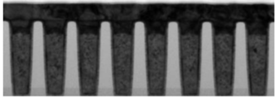
Figure 1. Transmission electron microscope image showing the deep-trench capacitor structure used to characterise the MIM stacks.
This type of testing requires careful attention to measurement methods. Under actual decoupling capacitor operation, where a constant bias voltage experiences small disturbances, the material shows remarkably stable capacitance independent of disturbance voltage, hold time, or number of pulses applied. The ferroelectric capacitors deliver 60 to 80 fF/μm² depending on operating voltage. Extensive reliability testing under various voltage levels, elevated temperatures of 90 degrees Celsius, and extended operation exceeding 400,000 seconds demonstrated negligible capacitance drift.
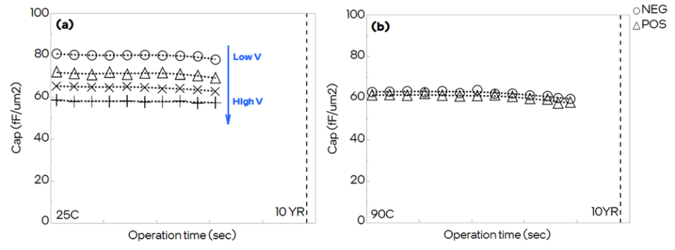
Figure 2. Capacitance measurements showing HZO’s stable, reliable performance under actual decoupling capacitor usage conditions.
Achieving Ultra-High Capacitance with Advanced Dielectric Materials
Titanium oxide and strontium titanium oxide provide even higher capacitance through extremely high dielectric constants with minimal voltage dependency. TiO achieves approximately 80 fF/μm², while STO reaches 98 fF/μm² — the highest demonstrated capacitance density.
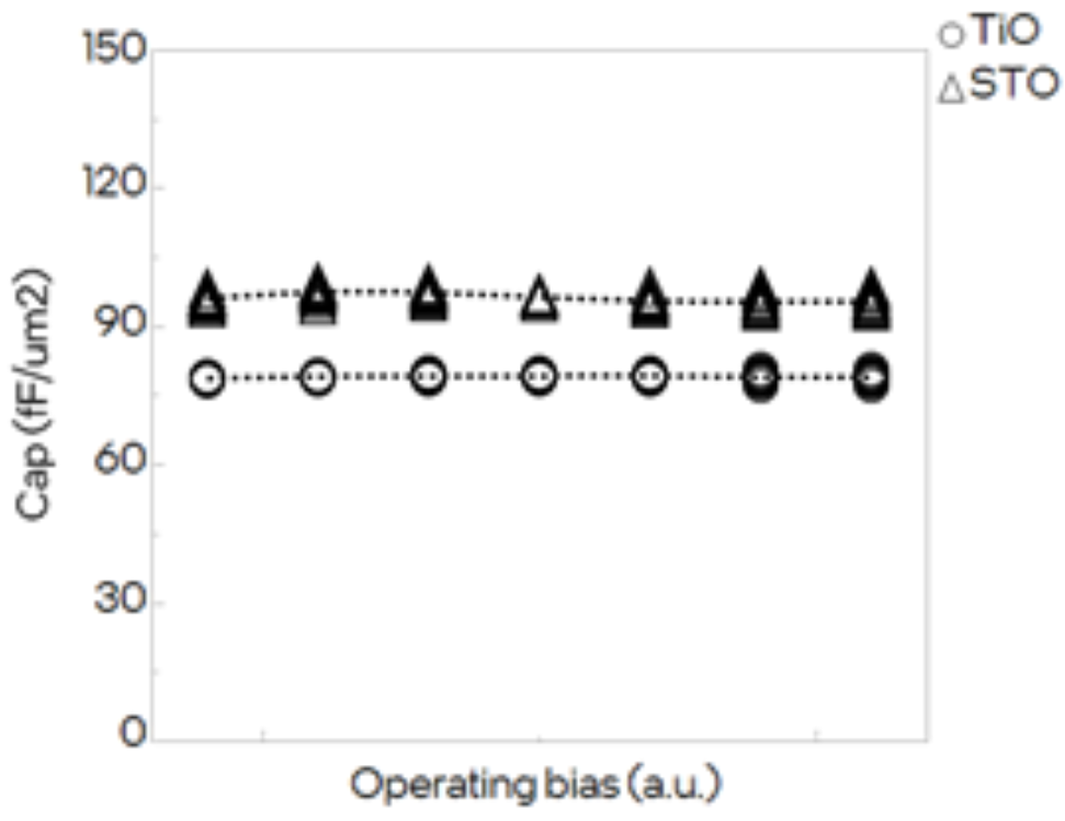
Figure 3. Capacitance versus voltage measurements showing weak voltage dependency across the operating range of interest.
Achieving these performance levels requires precise control over material structure at the atomic scale. The team developed optimised processes, including templating layers that guide crystal growth, controlling film deposition, thermal annealing that promotes desired crystal structure, and interface engineering to minimise defects. X-ray diffraction confirmed the successful production of strong high-dielectric-constant phases in both materials.
For TiO, detailed analysis reveals leakage current follows the Poole-Frenkel mechanism, where electrons trapped at defects gain energy from the electric field and hop between trap sites. This explains why the material withstands high currents without breaking down, with stress-induced leakage behaviour providing self-limiting protection against premature failure.
Exceptional Reliability Enables Multi-Layer Integration
All three materials demonstrate reliability exceeding decoupling capacitor requirements. Leakage current remains below targets even at 90 degrees Celsius. This is achieved through improved dielectric properties rather than making insulators thinner, which would increase leakage.
Time-dependent dielectric breakdown testing stressed devices at higher voltages and elevated temperatures, using statistical models to extrapolate expected lifetime. For HZO, extrapolation predicts operation exceeding high-voltage target spec for 10 years at 90 degrees Celsius with nearly identical breakdown behaviour regardless of voltage polarity. TiO also shows an extrapolated 10-year operating voltage significantly exceeding high-voltage requirements.¹ STO passes reliability targets for lower-voltage applications, though with larger variation due to deposition tooling requiring further optimisation.
The symmetric breakdown behaviour of HZO enables cost-effective multi-layer stacking where multiple capacitor layers connect in series, multiplying total capacitance without requiring complex integration schemes.
Looking Forward: Enabling Next-Generation Computing
This research demonstrates a clear path for continuous decoupling capacitor improvements across multiple semiconductor generations without increasing integration complexity. By improving intrinsic material properties rather than relying on structural innovations like deeper trenches or more layers, these approaches maintain manufacturing feasibility while delivering substantial performance gains.
The three materials provide flexibility for different requirements. HZO offers a practical, near-term option with reliability and straightforward integration. TiO serves as a successor with higher capacitance and exceptional high-voltage capability. STO represents the ultimate capacitance density for applications prioritising maximum capacitance.
Future work will focus on optimising these materials for manufacturing integration, refining deposition processes to improve uniformity, and exploring multi-layer stacking strategies. As computing advances toward AI accelerators, high-performance processors, and energy-efficient data centres, these capacitor technologies will play a vital role in enabling stable power delivery for next-generation semiconductor devices.
The post Intel Foundry Advances Chip Power Delivery with Next-Generation Capacitor Technology appeared first on ELE Times.
Keysight Partners with 3dB Labs to Enable Interoperable Signal Monitoring and Analysis
Keysight Technologies announced the integration of its spectrum analysers and FieldFox handheld analysers with 3dB Labs’ Sceptre, expanding interoperability between signal monitoring hardware and analysis software. The collaboration enables teams to monitor, analyse, and record radio frequency (RF) activity across mixed receiver environments within a unified workflow.
Teams operating in dense and contested RF environments often rely on equipment from multiple vendors while needing a consistent way to observe and interpret spectrum activity. By enabling Keysight instruments to operate directly within the Sceptre software environment, the integration reduces friction between measurement hardware and signal analysis workflows —allowing organisations to maintain multi-vendor receiver architectures while gaining a common platform for signal monitoring and investigation.
Sceptre supports real-time and offline spectrum and temporal analysis and connects receivers deployed on stationary or mobile collection platforms. When paired with Keysight analysers, users can monitor and characterise signals as they appear, capture activity for later playback, and analyse unknown or interfering signals to determine their nature and behaviour. The platform also supports unattended and remote operation, making it suitable for long-duration monitoring, RF surveys, and post-event analysis where access may be constrained.
Together, Keysight and 3dB Labs aim to strengthen the broader signal analysis ecosystem by promoting interoperability between measurement hardware and software-defined receiver platforms. Beyond improving day-to-day operations, the collaboration supports the development of more adaptable signal workflows, encourages integration across traditionally siloed tools, and helps teams build expertise that evolves as signal environments and mission demands change.
Dave Evans, President, 3dB Labs, Inc., said: “We are excited to partner with Keysight and integrate with their FieldFox handheld analysers, bringing Sceptre’s powerful signal detection, identification, and analysis capabilities to the tactical edge. We designed Sceptre for maximum interoperability, enabling teams to move from signal data to decisive action without bottlenecks, and together, we’re delivering an integrated solution that turns advanced signal processing into immediate mission advantage.”
Eric Taylor, Vice President of Aerospace, Defence and Government Solutions, Keysight, said: “Operational environments demand interoperability. By integrating Keysight analysers into multi-vendor ecosystems, teams can spend less time managing tools and more time understanding the spectrum. This integration brings together two leaders in the industry —Keysight in RF measurement and 3dB Labs in signal intelligence — to deliver advanced signal monitoring and analysis capabilities for our customers.”
The post Keysight Partners with 3dB Labs to Enable Interoperable Signal Monitoring and Analysis appeared first on ELE Times.
The story of 10 years, 10 PCBs, and everything I got wrong building a WiFi sub-PPB clock sync device
 | Story time submitted by /u/johny1281 Let me tell you a story about how a simple idea turned into a 10 year obsession. The end result is a tiny (4cm x 4cm) battery-powered node that syncs its clock to other nodes over the air with sub-PPB accuracy. No cables between them. You drop them wherever you want and they self-synchronize. I use it for phase-coherent Wi-Fi measurements across multiple receivers, which lets you do things like angle-of-arrival estimation and indoor localization. But getting here was not pretty. Board 0: The Aliexpress dev kit. I just finished my master's thesis and I've never made a PCB. I grab two ESP32 dev kits, learn how to flash them, learn how to capture Wi-Fi phase data. The data is pure noise. I spend months staring at random numbers before I understand why. Turns out a 10 ppm crystal gives you about 24 full phase rotations between consecutive Wi-Fi frames. Indistinguishable from random. Cool. Board 1: The Chinese flasher board. Before spending real money on a custom PCB I want to make sure I can flash bare ESP32 modules. Got this little Chinese jig, drop the chip in, flash over UART. Works first try. Good confidence boost. Still a garbage clock though. Board 2: First custom PCB ever. This is the big jump. Real money, real components, real chance of screwing up. EasyEDA, auto-router, fingers crossed. I try hand soldering the first batch and destroy every single one. Switched to solder paste and a $30 hot plate. Suddenly everything works beautifully. Same garbage data, but at least I stopped burning money on dead boards. Baby steps. Board 3: The "just share the clock" idea. Upgraded to a 0.5 ppm TCXO and tried to share it between two chips via jumper wires. Seemed so obvious. The parasitic capacitance of even short wires killed the signal dead. Touching a finger near the wire did the same thing. On the plus side, I discovered that the ESP32-C3 has hidden nanosecond RX timestamps buried in the firmware structs. That discovery ended up being the foundation of everything later. Board 4: The SMA cable attempt. Proper 50 ohm coax should fix the clock distribution problem, right? Somehow worse than bare wire. Also picked a clock buffer where the oscillator output was below the CMOS input threshold, so the buffer did literally nothing. Most expensive useless board of the project. Board 5: Two chips, one PCB, as close as physically possible. If cables don't work, just put the oscillator millimeters from both chips. No wires, no connectors, just traces. And it worked! First time I ever saw coherent phase. But the PCB antenna couldn't transmit (2-layer board, matching was completely wrong), and I measured about 1 ppb drift between two chips sitting 5mm apart. Thermal gradients. They're not at exactly the same temperature even when they're neighbors. Board 6: Scale to four chips. Got ambitious. Shared the voltage regulators because I didn't know you can't parallel LDOs. Only 2 out of 4 would boot. External SMA antennas made it the size of a shoebox. Back to the drawing board. Board 7: Remove the ground plane under the clock. Read somewhere online that ground pour causes interference near clock lines. Removed it. Everything got worse. Missing edges on the scope. Noise everywhere. Put it back. Don't believe everything you read. Board 8: Four layers, proper matching. Finally understood why every app note says 4 layers. On a 2-layer board the signal-to-ground distance is too large, coupling is loose, trace dimensions make no sense. On 4 layers everything behaves like the textbook. All 4 chips synced. But all 4 PCB antennas were coupled through the shared ground plane. PCB antennas use the ground as part of the radiating structure. Shared ground = shared antenna. Touching one killed the others. 20 dB down from a reference module. Board 9: Stop sharing clocks entirely. The breakthrough. Give each node its own voltage-controlled oscillator. Measure drift over the air using Wi-Fi timing exchanges. Correct with a DAC on the oscillator's tuning pin. One DAC got me to 10 ppb but each step was too coarse. Added a second DAC in a 1:30 ratio, coarse to get close, fine to hold steady. Sub-PPB. No shared ground, no coupled antennas, no cables. Each node is 4cm x 4cm and battery powered. Board 10: ESP-PPB. A few more boards in between with minor tweaks, but the big addition was the dual-DAC setup. 1 ppb typical in the open. 0.1 ppb in a stable enclosure, which is the measurement floor of the hardware. Oh and one more fun discovery: the radio silently compensates for frequency mismatch between sender and receiver internally. If two boards don't land on the same correction value, your data is garbage and you won't know why. With synced clocks they always agree. With unsynced clocks it's a coin flip. That one cost me months. Everything is open sourceEverything is open source. Firmware, schematics, Gerbers, BOM, 3D model. There's a story.md in the repo with photos of every board and what went wrong each time: https://github.com/jonathanmuller/esp-ppb Ask me anythingWhat was hardest, what was easiest, what I'd redo completely. This has been my side project for a decade and I'm happy to talk about any of it. [link] [comments] |
India to Boost Local Chip-making with a 1 Trillion Rupees Funding
India is expected to unveil a funding of more than a trillion rupees, nearly $10.8 billion, to fuel domestic chip-making. With 10 projects already approved, India aims to become a global manufacturing hub in the near future.
This new set of funds is expected to provide subsidies for chip designing projects, supply chain developments, and manufacturing equipment. Currently, the plan is under evaluation and may see the green light in a couple of months.
With the accelerated demand for chips driven by the rise of AI and electronics, the market is evolving at an exponential rate. Under the current leadership, India aims to position itself at the top to meet global demand.
With companies like Micron, TATA, and Foxconn already building India’s chip ecosystem, the country is expected to be close to industry leaders such as Taiwan and the US by 2032.
The post India to Boost Local Chip-making with a 1 Trillion Rupees Funding appeared first on ELE Times.
OK, this book is awesome!
 | Every connector under the sun is here. Plus it has IC interconnects so this post is technically not breaking the rules :) Thanks Davide for this great resource! [link] [comments] |
Prototype HV DC buck converter running on a PCB I fabricated with a fiber laser
 | This is a quick prototype HV DC buck board I built using the fiber-laser PCB process I posted earlier. Still experimenting with trace limits and thermal performance, but it's working surprisingly well so far. [link] [comments] |
E-ink mp3 player
 | This is V2 of my e-ink DAP project, it has :
V1 horribly failed, here is what changed since then:
The firmware is still in very early stages, I still haven't implemented a ton of features that the hardware is capable of, like DSP, Bluetooth, etc. I also need 3D print the case in resin, so it doesn't look like this, I want to use transparent resin The whole project is open source: GitHub [link] [comments] |
SpiceCrypt: open-source decryption tool for LTspice-encrypted .CIR/.SUB model files
 | submitted by /u/jtsylve [link] [comments] |
USBpwrME
 | Every time i want to do an experiment in the lab and use USB power to my DUT i need to find a cabler with correct connector and thick wires enough for the purpose and then cut it :(:( to be able to connect it to my bench power supply. So finally i decided to solve this reoccurring issue with a universal adaptor that will solve all my challenges and stopping me cutting cable after cable. This led up to designing the small adaptor that fits most power boxes since it has moveable banana binding posts. I have added polarity protection and over voltage protection that can be disabled to make it flexible and pass thru voltages from 3-20V out to the USB-A and USB-C connector. I have also added charging negotiation circuits for both USB-A (up to 10W @ 5V) and USB-C (up to 15W@ 5V). The adaptor can handle up to 6A so it will work for most application!! I have worked a lot with heat managment and tried to keep low resistance in the current paths. When loading max the hottest component reaches around 85 degrees C in room temp [link] [comments] |
Digi-key; A small U.S. town grew a big company. Can it weather the tariff blizzard?
 | submitted by /u/1Davide [link] [comments] |
Weekly discussion, complaint, and rant thread
Open to anything, including discussions, complaints, and rants.
Sub rules do not apply, so don't bother reporting incivility, off-topic, or spam.
Reddit-wide rules do apply.
To see the newest posts, sort the comments by "new" (instead of "best" or "top").
[link] [comments]
Spent hours troubleshooting to find out I got my PFETs backwards qnq
 | I’m attempting to make an LED scoreboard for my cricket team using large 7‑segment LED displays. I want it to be battery powered, so I’m trying to reduce the power needed to run 6+ digits at once by using multiplexing. Each segment is connected to a high‑side switch, and the digits to the low‑side. That way I can turn on each digit by pulling it low, and only the segments held high will activate. The code I’m using runs on an Arduino, which talks to a cheap PCA8695 PWM board. That board connects to a custom MOSFET driver board that handles the high‑ and low‑side switching. Running code that worked fine in my prototype setup just gave me an epileptic strobing effect on all segments, which completely threw me. I spent hours probing with a multimeter, using the oscilloscope at work, and eventually started cutting “non‑essential” components off the board. Instead of getting an inverted 12 V PWM signal like I expected, I was constantly getting a square wave oscillating between 12 V and 11.5 V no matter what I did. I was about to post on r/AskElectronics for help, but I wanted to be 110% sure I wasn’t missing something obvious. So I went to falstad.com and built the circuit in the simulator. Sure enough, it behaved exactly how I expected. Then I noticed a little checkbox for “Swap D/S,” and out of curiosity I clicked it… bingo. For testing, I’m going to desolder the PFETs I’ve got and jankily wire them in upside‑down just to confirm that’s the issue before ordering new ones. Moral of the story: make sure you’re using the right datasheet for your parts, because manufacturers love reusing part numbers even when the pinouts are completely different. (p.s. pls don't be too mean about diagram conventions, signal noise, etc. cos this is a self-taught learning exercise and I'm trying my best) [link] [comments] |
30-minute PCB fabrication with a fiber laser (double-sided boards)
") | I've been experimenting with using a fiber laser to fabricate prototype PCBs. Current workflow: - design PCB - laser isolate traces - drill vias - clean - solder Total time from design to board is about 30 minutes. Trace pitch so far is around ___ mil and I've been able to do reliable double-sided boards. I made a video showing the full process and the relaxation oscillator circuit I designed for it: [link] [comments] |
Exploration Alternatives of Component Marketplaces
 | The goal was to find where to buy electronics that i need(STM32F103C8T6 and STM32F401RET6), but figured it will be cool if i put all that in one post. Maybe someone finds it interesting. [link] [comments] |
IFW Dresden selects Agnitron Agilis 100 MOCVD platform for precursor chemistry and ultra-wide-bandgap materials development
Сторінки


![[link]](https://i.redd.it/6yqak75tz9pg1.png)