


Збирач потоків
Inflatable Robotic Dinosaur: The T. rex You Assemble Yourself
КПІ та Польща посилюють співпрацю у сфері безбар’єрності та ветеранської підтримки

🤝 У КПІ ім. Ігоря Сікорського відбулася зустріч із головою правління 🇵🇱 Фонду підтримки осіб з інвалідністю «Фроня» (Республіка Польща) — паном Алеком Вашкелевичем, який має 20-річний досвід роботи у питаннях доступності та глибоку експертизу у впровадженні принципів безбар’єрності в державному управлінні й університетському середовищі.
Infineon Supplies Silicon Carbide Technology to Fox ESS, Aims to Enhance Residential Energy Storage Efficiency
Infineon Technologies is now supplying silicon carbide (SiC) power semiconductors to Fox ESS, a renewable energy solution provider, to enhance the efficiency of its residential energy storage systems (ESS). Leveraging Infineon’s CoolSiC MOSFETs 1200 V G2 in the Q-DPAK package, Fox ESS has reduced switching losses by 70%. As a result, the company’s PQ3-Ultra energy storage system achieves a peak photovoltaic (PV) inverter efficiency of up to 98.78% in grid-tied operation and a peak battery charge/discharge efficiency of up to 98.47%.
“With our SiC MOSFETs in the Q-DPAK package, we are enabling a new level of efficiency, thermal performance and design flexibility for residential energy storage systems,” said Amit Raut, Application Manager Photovoltaic and Residential ESS at Infineon. “Fox ESS is demonstrating how advanced SiC technology can translate into measurable system-level gains and support the broader adoption of clean energy solutions in homes worldwide.”
Compared with conventional bottom-side-cooled designs, the Q-DPAK package supports improved PCB layout, helping to reduce parasitic effects and stray inductance while enabling superior thermal management. Its compact footprint supports space-saving system designs, while compatibility with automated assembly simplifies cost-efficient, scalable manufacturing.
Silicon Carbide Technology for High-Performance Energy Storage SolutionsWithin Fox ESS’s energy storage system, Infineon’s CoolSiC MOSFETs 1200 V G2 in the top-side-cooled Q-DPAK package deliver optimised thermal performance, system efficiency and power density. Infineon has specifically designed the devices for demanding applications requiring high performance and reliability. Featuring Infineon’s advanced .XT interconnection technology, they reduce thermal resistance and operating junction temperature, while the trench gate architecture helps lower switching losses.
“The collaboration with Infineon is a major pillar of our strategy to deliver high-performance energy storage solutions,” said Daniel Deng, R&D Director at Fox ESS. “Infineon’s CoolSiC technology offers superior efficiency and outstanding reliability, values that perfectly match our philosophy. By working together, we will further advance the performance of residential energy storage systems and accelerate the adoption of renewable energy.”
For its hybrid ESS solution combining the PQ-H3-Ultra-10.0 inverter with the EQ3300-5 battery, Fox ESS has achieved a System Performance Index (SPI) of 97.0 percent in a recent test by HTW Berlin University of Applied Sciences and AQUU Research. This ranks Fox ESS first in the 10-kW class among all hybrid inverter and storage systems tested in 2026 and marks the highest SPI score recorded since the evaluation was launched in 2018. Over the past three years, Fox ESS has installed more than 890,000 PV inverters and over one million batteries in more than 70 countries.
The post Infineon Supplies Silicon Carbide Technology to Fox ESS, Aims to Enhance Residential Energy Storage Efficiency appeared first on ELE Times.
DPOT push up/down

Some folks prefer pushbutton switches to take effect on push instead of release. These buttons do that very thing.
I suppose it’s really just a matter of taste, but I’ve always liked momentary contact switches that act when you push them better than those that wait until you let go. It’s really an arbitrary thing, so I wouldn’t presume to criticize designs that choose the latter over the former, like this one from one of my favorite Design Idea contributors.
It’s not worse. Or better, for that matter. Just different.
Wow the engineering world with your unique design: Design Ideas Submission Guide
In contrast to RJ’s design, Figure 1’s circuit implements my preferred method. It bumps DPOT U2’s setting by one count each time the UP button is pressed, and un-bumps it when DOWN is mashed.

Figure 1 This pushbutton-to-digital-potentiometer interface is optimal for impatient people.
Here’s how it works.
Pushing either button makes U1a’s pin 3 go high. Contact bounce is filtered out by R3C1’s ~5 ms time constant, and Schmidt trigger inverter U1d then delivers a single clean low-going transition to U2’s clock input. This makes U2’s wiper take one step up if its pin 2 is high (i.e., the UP button is pressed and DOWN isn’t) or one step down if pin 2 is low (i.e., DOWN is down).
Other than that difference, there’s really no compelling reason to choose Figure 1 over RJ’s circuit. Figure 1’s parts count does include one fewer chip, but so what? They’re cheap.
But stay tuned for future developments that go-when-pushed makes possible, which might be more significant…
Stephen Woodward‘s relationship with EDN’s DI column goes back quite a long way. Over 200 submissions have been accepted since his first contribution back in 1974. They have included best Design Idea of the year in 1974 and 2001.
Related Content
- Push to increase, decrease a digital potentiometer
- Keep Dpot pseudologarithmic gain control on a leash
- Synthesize precision Dpot resistances that aren’t in the catalog
- Op-amp wipes out DPOT wiper resistance
- PWMpot approximates a Dpot
The post DPOT push up/down appeared first on EDN.
Cree LED and Nanolumens enter settlement and limited patent license agreement
India Semiconductor Mission 2.0: Bolstering India’s Technology Prowess
– Anwesh Koley, Executive Editor, ELE Times
The government is serious about making India a global technology hub and how! After the visible success of the first phase of the India Semiconductor Mission, policy makers are walking the talk with the 2nd phase of the India Semiconductor Mission (ISM 2.0). In a move that could well be termed monumental, a staggering Rs 1,27,500 crore (around $13.25 billion) has been approved towards building an integrated semiconductor ecosystem across major Indian states.
The Indian semiconductor market is currently valued at around $45–$50 billion and is expected to expand to $100–$110 billion by 2030. At a time when India is working to strengthen its position in the global semiconductor supply chain, Semicon 2.0 is expected to provide a significant boost to India’s electronics and semiconductors industry. The emphasis of ISM 2.0 will be on deepening the country’s semiconductor and design ecosystem.
A Resilient Pursuit of Indigenous Capacity ExpansionWhat stands out is how Semicon 2.0 builds on the foundation laid by ISM 1.0. While the first phase focused on establishing India’s semiconductor base through ecosystem creation, ATMP/OSAT and early project execution, Semicon 2.0 is notably broader in scope – spanning chip design IP, equipment and materials, fabs, advanced packaging, R&D and talent development. While much of the conversation around chips has focused on fabrication plants, the latest developments indicate that India is building a broader ecosystem that includes packaging, testing, display manufacturing, and advanced materials.
Airing his views on phase 2 of the ISM, Amitesh Kumar Sinha, CEO, ISM, said, “As India’s semiconductor journey has already gathered momentum, the India Semiconductor Mission (ISM) has laid a strong foundation for semiconductor manufacturing in India, with 10 approved projects—including 2 fabs and 8 ATMP or OSAT units—attracting investments of around Rs 1.6 lakh crore. With ISM 2.0, the focus now shifts to deepening the value chain across materials, equipment, IP, and supply chain resilience.”
Harnessing Global EfficienciesAs India moves decisively from semiconductor policy to on-ground execution, ISM 2.0 provides a structured pathway to leverage the strengths of global partners in advanced manufacturing, supply chain integration, and design, while accelerating India’s capabilities across assembly, testing, packaging, the broader component ecosystem and overall Semiconductor ecosystem.
India sees strong potential for deeper participation from South Asian countries like Singapore across the value chain. “I would like to assure that ISM is all set to support any further investments in the sector. We are fully committed to facilitating and supporting such investments—ensuring a trusted, scalable, and globally competitive semiconductor ecosystem anchored in strong international partnerships,” affirmed Sinha.
As countries continue to diversify global chip supply chains, India’s semiconductor roadmap is increasingly viewed as a long-term manufacturing and strategic play rather than a short-term production target. India’s world-class engineering talent is a proven asset, and sustained R&D investments are expected to further elevate its position in the global supply chain.
What’s New in ISM 2.0
Finance Minister Nirmala Sitharaman announced ISM 2.0 in the Union Budget 2026, with an initial emphasis on design, equipment and materials. The announcement confirmed that Semicon 2.0 will broaden this framework further, encompassing design, machines and materials, fabs, the strengthening of ATMP/OSAT capabilities, research and development, and, significantly, talent development.
Indian Semiconductor Mission 1.0 focused on setting up basic chip making and packaging factories with a budget of Rs 76,000 crore. Taking this initiative a step further, Indian Semiconductor Mission 2.0 expands and strengthens the whole supply chain with a budget of Rs 1,27,500 crore. Indian Semiconductor Mission 1.0 made progress with 12 manufacturing units with investments over Rs 1.64 lakh crore. 24 Semiconductor design projects from startups have been approved for financial support while 105 startups have been granted access to EDA tools.
Under Indian Semiconductor Mission 2.0 government financial support is structured to deepen and strengthen the domestic value chain. For example, subsidies up to 40% on silicon fabrication plants and subsidies up to 35% on other fabrication plants. Semicon 2.0 is more diverse and deeper than ISM 1.0 because of the massive budget, focus on the semiconductor ecosystem, industry-led research and development centers and training programs, which lay the foundation for resilient supply chains and high value employment.
ISM 1.0 delivered approvals, investments, and early commercial production. Semicon 2.0 is aimed at deepening domestic capability across the value chain, from materials and equipment to advanced packaging, R&D, and skilled talent. If Semicon 1.0 was about proving that India can enter semiconductors, Semicon 2.0 is about proving that India can scale them.
The ISM (1.0 and 2.0) is critical for India Inc, because the growth of semiconductor supply and ecosystem is highly essential for India to build and grow its own microchip and semiconductor industry. This goes a long way in reducing foreign reliance, encouraging local and domestic industries, economic growth, employment, education, skill based teaching and national security. These foundational capabilities shield the country from global disruptions and foster sustainable, high value technical industries.
Key Components of Semicon 2.0The Rs 127,500 crore initiative is a comprehensive push to build India’s semiconductor capabilities for the long term. Hailing this budgetary approval, Hitesh Garg, Vice President and India Managing Director, NXP Semiconductors, said, “As India progresses toward the vision of a “Viksit Bharat” by 2047, the Union Budget will be a critical lever in shaping the country’s medium- to long-term growth trajectory—particularly as global supply chains diversify and technology-led manufacturing becomes central to economic resilience and national competitiveness.”
Since ISM 1.0, the key focus has revolved around talent development, supply-chain readiness, access to raw materials, and long-term competitiveness against established semiconductor hubs. ISM 2.0 framework is expected to address some of these gaps by supporting equipment, chemicals, design ecosystems, and research capabilities. The key focus areas of Semiconductor 2.0 are broadly based on six pillars:
1) Design: The first pillar is based on chip design. Under phase 2, the aim is to develop designs of chips and systems and IPs. ISM 2.0 will focus on designing full stack Indian semiconductor intellectual property, and fortifying both domestic and global supply chains
2) Machines and Materials: Companies and Industries that are involved in the manufacturing process and research and development of machines, materials, chemicals that are essential for manufacturing semiconductors will be encouraged.
3) Setting up more fabrication plants: Efforts will be made to attract more manufacturers to come to India and set up fabrication plants to manufacture chips. Fabrication plants like silicon, compound semiconductor, display etc.
4) Strengthening the ATMP (Assembling, Testing, Marking and Packaging) industry: Setting up of ATMP/ OSAT units is encouraged for strengthening the semiconductor supply chain. Several approved proposals aim to leverage indigenous technologies for the assembly, testing, and packaging of semiconductor chips.
5) Research and Development: Research and Development of semiconductors is essential for advanced technological mechanisms to create better, faster electronic devices. The focus is on developing more advanced nodes and advanced technologies within and outside India.
6) Talent development: Talent development in semiconductors is the process of educating, training, and upskilling people to build a skilled workforce for chip design, manufacturing, testing, packaging, and research. With 315 universities training students using the latest EDA tools, about 68,000 students have already been trained.
“Government initiatives such as ISM 2.0 are a defining milestone in India’s journey toward global semiconductor leadership. By expanding support across the entire value chain from manufacturing and advanced packaging to critical materials and design, this initiative builds a foundation for long-term competitiveness,” Garg opined.
India Semiconductor Mission 2.0: Why it Stands Apart
By structuring Semicon 2.0 around six key pillars, the government has taken a holistic view of the industry. The clear roadmap that the sector’s future lays out is especially commendable. This is not merely about setting up a few fabs; it is about building the foundation for India’s semiconductor future over the coming years. While achieving this vision will require sustained effort, collaboration, investment, and strong industry-government partnership, the direction remains clear.
Airing his optimism for phase 2, Vinay Shenoy, MD, Infineon Technologies, India, said, “ISM 2.0 marks a decisive step in India’s journey from semiconductor consumer to semiconductor innovator. For Infineon, having invested in India’s ecosystem for over 25 years, this signals strong policy continuity and ambition. The enhanced focus reinforces our belief that India has the talent and capabilities to further strengthen its position as a global hub for chip innovation, particularly in areas driving decarbonization and digitalization.”
Policy AssuranceThe government’s recent approvals, including projects in Gujarat, Odisha, Assam, and Uttar Pradesh, reflect a shift from policy announcements to infrastructure creation. Companies such as Tata Electronics, Micron, CG Power, and Kaynes Semicon are now part of a growing domestic semiconductor network that aims to reduce import dependence and strengthen India’s role in global electronics manufacturing.
NXP’s Garg further reiterated the semiconductor manufacturer’s commitment towards this massive capacity-building initiative. “At NXP, we are fully committed to this vision. We continue to advance cutting-edge R&D locally and nurture future-ready talent. We believe that collaborative ecosystem innovation is the key, and we look forward to partnering with industry, academia, and policymakers to drive India’s emergence as a global semiconductor hub.”
What makes this phase significant is the focus beyond just fabs. Advanced packaging technologies, display assembly, compound semiconductors, and supply-chain support systems are emerging as equally important areas. Industry observers believe this approach could help India gradually build capabilities in sectors linked to automotive electronics, telecom, AI hardware, and industrial devices.
Conclusion: A Robust Framework for India Semicon IncThrough Semicon 2.0, India is demonstrating its readiness to emerge as a trusted and resilient partner in the global semiconductor value chain. The long-term policy support and substantial investment approved by the Cabinet underscore India’s determination to advance domestic capabilities and attract world-class semiconductor manufacturing to the country.
Semiconductor technology is at the heart of all critical technologies and India must catch up with the global leaders in this domain. Strategic strength and ability to lead development of new technologies, R&D and emerging areas of expertise cannot be achieved without electronics and semiconductors. ISM 2.0 is a timely move that will take us to the next level and deliver immense social and economic benefits for India.
This landmark announcement strengthens India’s backend semiconductor capabilities by enabling large-scale production of discrete chips tailored to high-growth sectors such as electric vehicles and industrial automation. Little wonder then, that as time progresses, India’s electronics and semiconductor ecosystem is steadily advancing towards becoming a self-reliant and globally competitive manufacturing hub.
The post India Semiconductor Mission 2.0: Bolstering India’s Technology Prowess appeared first on ELE Times.
Trymax secures multi-million-dollar supply agreement with AOI to support InP laser manufacturing
AmpliTech’s AGMDC division wins orders for three custom GaAs components
A 4-step guide to selecting PFC conduction mode: CrM/DCM vs. CCM

The power factor correction (PFC) boost converter is the industry-standard topology for meeting harmonic current regulations such as IEC 61000-3-2. This circuit is essential in modern AC/DC power supplies, where it shapes the input current (IIN) to follow the input voltage (VIN) sinusoidal waveform, achieving a power factor near unity.
The key to successful PFC design lies in its operating mode. While three basic modes exist—continuous conduction mode (CCM), discontinuous conduction mode (DCM), and critical conduction mode (CrM)—the fundamental design choice is between a system built for CCM and a system optimized for CrM. A controller designed for CrM naturally operates in DCM at lighter loads, meaning CrM and DCM are often analyzed together as a single design path (CrM/DCM).
Selecting between CCM and CrM/DCM presents a fundamental trade-off that directly impacts the converter’s efficiency, physical size, cost, and EMI performance.
Figure 1 shows the typical PFC boost converter schematic.

Figure 1 A typical PFC boost converter schematic shows the industry-standard topology for modern AC/DC power supplies. Source: MPS
Below is the 4-step guide to selecting PFC conduction mode. It provides a clear methodology for navigating the tradeoffs, beginning with the primary design constraint and culminating in an informed topology selection.
Step 1: Identify primary design constraint
Before analyzing technical specs, the primary design constraint must be defined, as this informs the rest of the decision-making process. Common design constraints include:
- Maximum power density: Make the power supply as small and compact as possible.
- Minimum cost: Reducing the BOM is usually the most critical design factor.
- Maximum efficiency: Target a specific efficiency rating, for example, 80 PLUS Titanium, where every fraction of a percentage point matters.
- EMI performance: The product is intended for a sensitive environment, for example, medical, avionics, or high-fidelity audio, where passing strict EMI regulations is a major challenge.
Once the primary design constraint is identified, the next step is to analyze core trade-offs.
Step 2: Analyze core trade-offs of selected power range
While the ideal conduction mode is heavily dependent on the application’s power range, it’s crucial to first understand the inductor current (IL) behavior in each mode, as this determines all other performance characteristics.
Figure 2 shows the fundamental difference between the IL waveforms of the PFC boost modes (CCM and CrM) across a few switching cycles around the peak of the line half-cycle, where the average inductor current (IL_AVG) is highest.

Figure 2 Note the fundamental differences between the IL waveforms of the PFC boost modes. Source: MPS
The IL behaviors in CCM and CrM are described below:
- CCM: IL always remains above 0 A and has a relatively small triangular ripple current superimposed onto a large average inductor current (IL_AVG).
- CrM: IL is a series of triangles, where each cycle begins at 0 A. The current ramps up to a peak, then ramps back down to 0 A, at which point the next cycle immediately begins.
For selecting component stress and size, the peak switching current (ISW_PK), required inductance (LPFC), and dominant power losses must be calculated. These calculations are typically evaluated at the peak of the low-line AC input voltage (for example, 85 VAC), which represents the worst-case scenario for the RMS inductor current (IL_RMS) and peak inductor current (IL_PEAK).
Peak Switching current
ISW_PK determines the required current rating of the MOSFET and diode. The baseline for comparison is the average input current at the sinusoid peak (IIN_PK_AVG).
The CCM peak switching current (ISW_PK_CCM) can be calculated with Equation (1):

Where IIN_AVG is the average input current, and KR is the ripple factor (typically between 0.2 and 0.4).
The CrM peak switching current (ISW_PK_CRM) can be calculated with Equation (2):

The peak current flowing through the switch and diode in CrM is about twice the peak current in CCM for the same input power (PIN). This directly impacts conduction loss (I2R).
Required inductance
LPFC determines the main magnetic component size. The required CCM inductance (LPFC_CCM) can be calculated with Equation (3):

Where DPK is the duty cycle at the peak input voltage (VIN_PK), and fSW is the switching frequency.
The required CrM inductance (LPFC_CRM) can be calculated with Equation (4):

The required boost inductance depends strongly on the target ripple current and fSW strategy. In many practical PFC designs, CCM uses a higher inductance to limit current ripple, while CrM can use a lower inductance at the expense of higher peak and RMS current.
Dominant power losses
Efficiency requires a trade-off between conduction loss and switching loss. Table 1 shows the dominant power losses in CCM compared to CrM/DCM.

Table 1 Here is a comparison of dominant power losses in CCM vs. CrM/DCM. Source: MPS
Based on Table 1, CCM reduces conduction loss with the disadvantage of high switching loss, meanwhile CrM eliminates the worst switching losses with the disadvantage of higher conduction loss. This understanding can be applied to different power ranges.
For low-power applications below 200 W, CrM/DCM is preferred. The high switching loss in CCM (from IRR) is the dominant factor for power loss, which is eliminated in CrM. This leads to higher overall efficiency. For high-power applications exceeding 400 W, CCM is preferred. The total current is high enough to result in massive conduction losses from the IRMS2 penalty in CrM. These IRMS2 x RDS(ON) losses far outweigh the advantages of lower switching loss, meaning CCM is more efficient overall.
Step 3: Verification using design decision map
A visual decision map can be used for verification by plotting the output power (POUT) against typical switching frequencies (see Figure 3).

Figure 3 A PFC mode design decision map (CrM/DCM vs. CCM) can be used for verification. Source: MPS
The ideal operating regions for each mode are described below:
- CrM/DCM recommended (green region in Figure 3): As established in step 2, when analyzing the core trade-offs, this region is ideal for CrM due to superior efficiency at light loads and lower cost.
- CCM recommended (red region in Figure 3): The lower conduction losses and smaller inductor size in CCM are ideal for high-power, high-density designs. Moreover, CCM offers advantages for conducted EMI and EMI filter designs due to its lower inductor current ripple and higher continuous input current.
- Transition zone (yellow region in Figure 3): The decision between selecting CrM/DCM and CCM depends on the primary design constraint identified in step 1.
Step 4: Select controller and explore alternatives
If a CrM/DCM controller is selected based on step 3, the design typically benefits from lower cost, good light-load efficiency, and reduced reverse-recovery-related switching stress.
If a CCM controller is selected based on step 3, using a fast-recovery or silicon carbide (SiC) boost diode can significantly reduce reverse-recovery-related losses and ease thermal design.
When selecting between a CrM/DCM and CCM controller, interleaved PFC architecture provides an alternative design that achieves higher performance, low switching loss, and EMI benefits. Interleaved PFC architecture can significantly reduce input current ripple and RMS current in both the input and output capacitors. This improves thermal stress and can reduce filtering requirements while preserving many of the switching loss advantages associated with transition mode.
Final design checklist
By following this 4-step guide to selecting PFC conduction mode, the correct topology can be selected according to the design specifications. A final checklist is provided below, summarizing the rules of thumb to keep in mind.
- If the power is below 200 W, select CrM/DCM.
- If the power exceeds 400 W, select CCM (with a SiC diode).
- If the power is between 200 W and 400 W, select the PFC conduction mode based on the primary design constraints defined in step 1:
- Cost or EMI: CrM/DCM
- Size: CCM
- Performance: Interleaved CrM
Final design
Designing the CrM/DCM PFC stage is based on the calculation of the boost inductance and the peak stress on key switching components. Table 2 shows the design results.

Table 2 These design results are based on the calculation of boost inductance and peak stress on key switching components. Source: MPS
Take the case of the MP44018A chip employed for the PFC stage as a multi-mode controller operating in CrM and DCM via the ZCD pin (Figure 4). It’s designed to provide high-performance active PFC with a minimal number of external components. This PFC controller’s very low supply current achieves low standby power loss, with a typical no-load power consumption below 30 mW.

Figure 4 Here is how CrM/DCM PFC boost works using the MP44018A controller. Source: MPS
Light-load efficiency is improved through dead-time extension technology, which reduces the switching frequency under such conditions. Furthermore, MP44018A achieves lower total harmonic distortion (THD) compared to conventional constant-on-time (COT) control by utilizing a variable-on-time control strategy while in DCM.
Figure 5 shows the measured input current harmonic spectrum at VIN = 230 VAC and POUT = 240 W in a compliance-oriented view of boost PFC performance. The red bars correspond to the harmonic content achieved by the implemented PFC solution with MP44018A. The blue bars show the applicable IEC 61000-3-2 harmonic current limits for the target equipment class.

Figure 5 The harmonics results are compared to IEC 1000-3-2 Class C compatibility standard. Source: MPS
A strategic approach to conduction mode selection
Implementing an active PFC front-end is a critical requirement for modern AC/DC power supplies to ensure high efficiency and compliance with harmonic current regulations. This article demonstrated that selecting the proper conduction mode is foundational for PFC construction, directly impacting the converter’s efficiency, physical size, cost, and EMI performance.
A strategic approach to conduction mode selection helps optimize the final design to meet its specific application targets, whether that is maximum power density, minimum cost, or peak efficiency. For designs that follow the CrM/DCM path, a multi-mode controller can provide an effective solution for achieving strong light-load efficiency and harmonic performance with a low external component count.
A PFC front-end with a stable DC bus provides an ideal foundation for a high-efficiency secondary stage. Pairing this PFC front-end with a resonant LLC converter is a particularly effective strategy, enabling high-performance and high-density power solutions for markets ranging from consumer adapters to industrial supplies.
Rafael Collado is a supervisor at Monolithic Power Systems (MPS).
Related Content
- Design interleaving PFC boost power stages
- How to design a digital-controlled PFC, Part 1
- How to design a digital-controlled PFC, Part 2
- How to design a digital-controlled PFC, Part 3
- How to design a digital-controlled PFC, Part 4
The post A 4-step guide to selecting PFC conduction mode: CrM/DCM vs. CCM appeared first on EDN.
Market for Securing AI Set to Reach $4.8 Billion in 2027: Gartner Report
The market for securing AI is growing rapidly, projected to reach almost $4.8 billion in 2027, a 68.7% increase over 2026, according to the latest Gartner report. By 2028, the market is forecast to reach almost $7.7 billion. AI application security will remain the largest AI security spending category in 2027.
Gartner predicts over half of successful cyberattacks on AI agents are expected to exploit access control weaknesses and prompt injections by 2029. There is a growing need for organisations to identify, monitor and protect AI models from these unique threats, which is driving the adoption of advanced AI security solutions. To build a strong defence, businesses need to combine their existing security systems with specialised AI security tools.
“This surge is driven by the urgent need for enterprises to secure AI systems, address emerging vulnerabilities and strengthen defences against sophisticated cyberthreats,” said Shailendra Upadhyay, Senior Principal Analyst at Gartner. “This is compounded by growing vulnerabilities and supply chain attacks involving third-party and open-source software in AI projects. Without adequate security and visibility controls, enterprise AI initiatives face a high risk of failure,” he added.
The market for securing AI is divided into four main areas: AI application security, AI usage control, AI governance platforms, and AI gateways. This includes a range of software and platforms designed to help organisations use AI safely, responsibly, and in line with regulations.
Market CompetitionAccording to Gartner, competition in the securing AI market varies depending on the segment. For AI governance platforms and AI gateways, which often build on existing enterprise systems for governance, data, and API management, major vendors are likely to maintain their lead by adding AI features or integrating specialised products. On the other hand, the AI application security and AI usage control segments are seeing a wave of startups entering the field.
“As the market grows, we can expect increased consolidation and acquisitions, with larger cybersecurity companies buying these startups to broaden their offerings,” said Upadhyay. “Overall, the fast-paced growth in this space is fuelling intense competition among vendors as they vie for market share.”
AI application security will remain the largest spending category in 2027 and is projected to reach almost $851 million, followed by AI usage control at $749 million. However, AI usage control will experience the largest growth of 73%, followed by AI gateway at 70.9%.
Securing AI Opportunity by Segment (Millions of U.S. Dollars), 2026-2027
| Segment | 2026
Spending |
2026
Growth (%) |
2027
Spending |
2027 Growth (%) |
| AI Application Security | 508 | 82.1 | 851 | 67.5 |
| AI Usage Control | 433 | 86.6 | 749 | 73.0 |
| AI Governance Platforms | 275 | 77.4 | 462 | 68.0 |
| AI Gateway | 251 | 80.6 | 429 | 70.9 |
| Other Securing AI | 1,368 | 83.9 | 2,292 | 67.5 |
| Total | 2,835 | 83.0 | 4,783 | 68.7 |
The post Market for Securing AI Set to Reach $4.8 Billion in 2027: Gartner Report appeared first on ELE Times.
Nuvoton to Showcase MCU/ MPU/ Audio, Battery Tech, Smart Sensing Solutions at Electronica 2026
Nuvoton Technology Corporation will demonstrate its latest advancements in HMI, audio, automotive technology, and smart energy management at Electronica India 2026. The company will showcase a comprehensive lineup of solutions designed to meet the evolving needs of the Indian market, focusing on smart buzzers, Cortex-M23 MCUs, Cortex-A35 MPUs, Arm9 MPUs, Gerda ICs, TOF sensing, and automotive and industrial BMICs.
Next-Generation Battery Management Systems (BMS)Nuvoton is highlighting its leadership in battery technology with several key demonstrations:
- Automotive Excellence: The KA84936UA evaluation solution offers high-precision cell voltage measurement (±1.5 mV accuracy) for up to 20 series-connected cells. Designed for ISO 26262-compliant safety systems and AEC-Q100 compliance, it is ideal for EV, PHEV, and HEV applications.
- Industrial High-Voltage Systems: The KA49703A stackable battery monitoring solution supports daisy-chain communication for up to 55 devices, making it a robust choice for high-voltage Energy Storage Systems (ESS) and data center backup power.
- Integrated Monitoring & Voice Support: The Battery Monitoring and Voice Prompt System, powered by the NUC980 MPU, features four CAN Bus interfaces for real-time monitoring of multiple battery groups, integrated with emWin graphics and voice-enabled fault responses.
Nuvoton continues to redefine user interaction with advanced display technologies:
- Two-Wheeler HMI: An integrated solution for next-generation two-wheelers featuring the Gerda IC series. This system boasts a rapid boot-up time of less than 0.5 seconds and high visibility under direct sunlight, all on a PCB the size of a business card.
- Industrial Energy Display: The MA35D1 MPU-based platform leverages the Qt5 framework to provide visualized interfaces for new energy applications, supporting multitasking and scalable expansion.
- Smart ITO Panel: A 20-key touch-panel reference design based on the M258 MCU for household appliances, such as rice cookers, demonstrating high sensitivity and simplified development via the NuTool-LCDView.
The technology company will also showcase its KW330 Series for robust human and object perception. Utilizing 2D and 3D sensing, the technology enables skeleton tracking, gesture recognition, and presence detection for applications ranging from automotive in-cabin monitoring to industrial human-machine collaboration.
Rounding out the display is the Power Delivery 3.0 Dual Role Power (DRP) solution based on the M2L31 MCU, which allows devices to switch seamlessly between power source and sink roles with up to 25W of power delivery. Additionally, the Smart Buzzer (NSP2340BA24E) offers an all-in-one voice chip solution with a built-in high-voltage driver for piezoelectric applications.
The post Nuvoton to Showcase MCU/ MPU/ Audio, Battery Tech, Smart Sensing Solutions at Electronica 2026 appeared first on ELE Times.
DLI Scheme-backed Aheesa and Zigma Join Hands to Distribute Indigenous Networking Chip
Aheesa Digital Innovations, a fabless semiconductor company, and The Zigma Technologies India, an Indian technology, software, and e-governance services company, have entered into a partnership with Zigma as the distribution partner to take VIHAAN-I, a first-of-its-kind indigenous networking chip, to market across India. Signed in the nation’s financial capital Mumbai, this agreement brings together Aheesa’s design capability with Zigma’s to carry indigenous silicon to the market across India and beyond.
The partnership follows Aheesa’s successful VIHAAN-I tape-out on Republic Day (January 2026) and first-pass silicon success in August 2026, achieved on its very first attempt. This chip will help reduce dependence on imported networking silicon and support locally manufactured broadband devices. Taking a chip like this into the country’s networks calls for a partner already embedded in the systems, and Zigma has spent close to three decades in precisely that terrain, delivering technology and e-governance infrastructure to OEMs, ODMs and government departments nationwide.
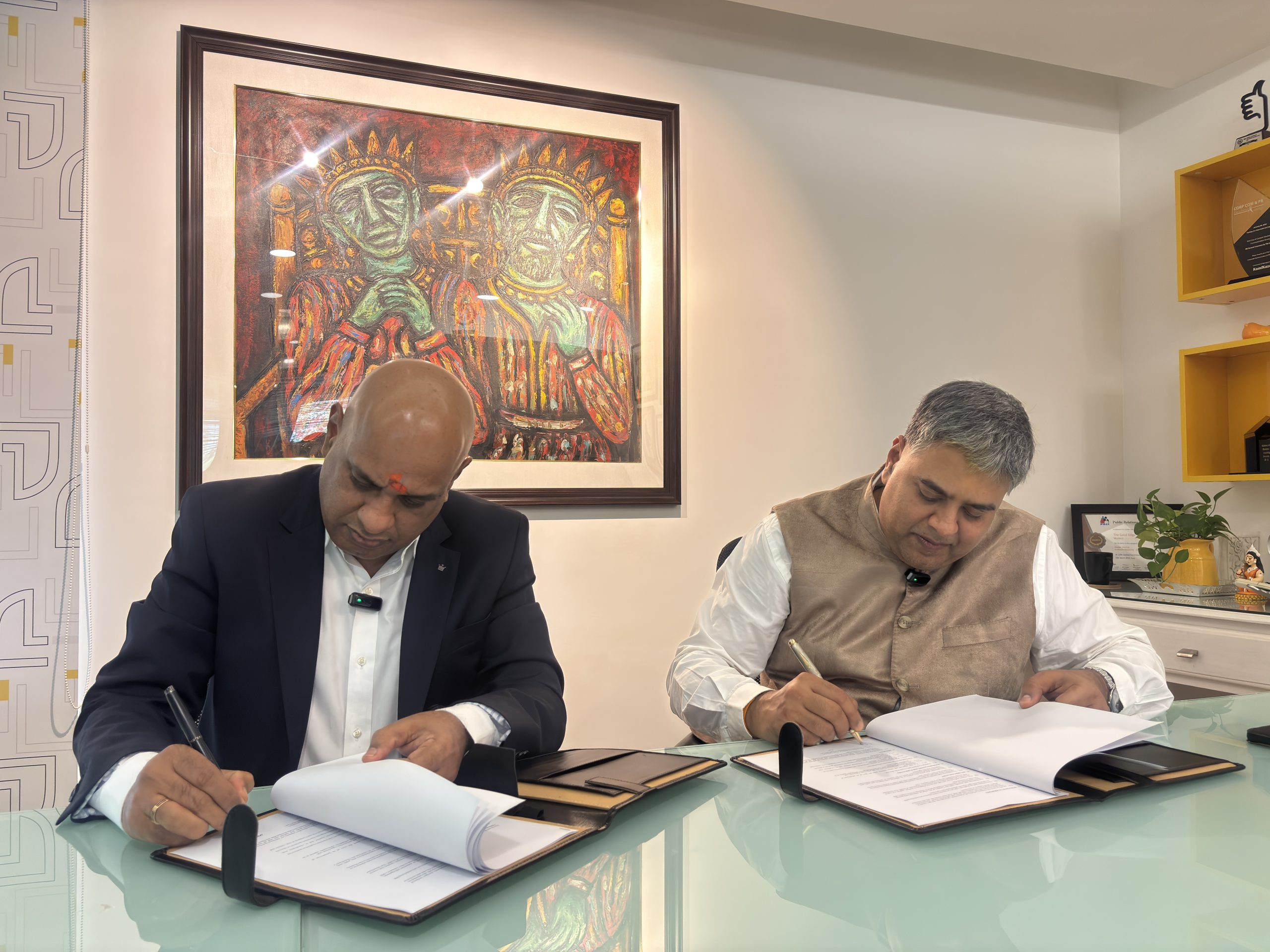
The chip will now proceed towards production, targeted for 2027. This will be a significant milestone in India’s efforts to build a homegrown semiconductor ecosystem, closely aligned with the Government of India’s Digital India and Atmanirbhar Bharat initiatives.
Augmenting Indigenous Semiconductor Technology“This is a defining decade for India’s semiconductor story, as we move from technology consumption to technology creation,” said Sridharan Mani, Founder and CEO, Aheesa Digital Innovations. “At Aheesa, we dream beyond boundaries — building the capabilities, scale and industry that will shape India’s semiconductor future. It is our vision to see Indian-designed chips serving both domestic and global markets. The partnership with Zigma brings together two companies with complementary strengths and a shared ambition for a Viksit Bharat.”
“Zigma has worked at the intersection of technology and public infrastructure, building the systems that carry India’s digital services to its people,” said Raja Kathiravan, Managing Director, The Zigma Technologies India (P) Limited. “Indigenous silicon is the natural next layer of that infrastructure. In VIHAAN-I, we saw a homegrown broadband chip we could take straight into the systems we help build and in Aheesa, a partner who shares our conviction about what Indian engineering can achieve. Together, we intend to put Indian silicon at the heart of the country’s digital backbone.”
The post DLI Scheme-backed Aheesa and Zigma Join Hands to Distribute Indigenous Networking Chip appeared first on ELE Times.
Apple’s processor cadence: A pending stutter-step for improved long-term edge inference?

Apple Silicon’s success track record is indisputably impressive. It’s also rife with implementation inconsistency, albeit reflective in no small part of broader industry status impermanence.
When Apple announced its computing platform migration from Intel x86 to homegrown Arm-based SoCs beginning in mid-2020, initial industry response was initially mixed. There was no shortage of schadenfreude, mind you, both considering that Intel had done the same thing to the IBM/Motorola PowerPC Alliance a decade and a half earlier, and more broadly Intel’s then-status as the predominant processor supplier to the computing segment. That said, and as was hopefully evident even in my earliest Apple Silicon era coverage, I was personally confident in the strategy’s sooner-or-later transition success, which is ironically winding up as we speak.
For one thing, Apple’s relationship with Intel was growing increasingly strained, as the chip supplier’s power consumption vs performance trends grew more worrisome, as new-product schedules slipped, and as the bugs in those products multiplied. For another, Apple and foundry partner TSMC (superseding initial partner Samsung) had for a while already been developing new SoCs for smartphones, tablets, smart watches and other devices. And then there’s Apple’s in-house vertical integration and control of both hardware and software, the latter spanning both operating systems and first-party applications and suites, as well as its exclusivity as provider of both developer tools and App Store approvals for third-party coders.
New life
And so here we are with today’s M6, the company’s latest mainstream SoC offering. It’s notable for being the premiere volume production implementation of TSMC’s newest 2 nm fabrication technology foundation. And Apple’s done (as well as, equally notably, not done) numerous things, most of them predictable but a few more surprising, with the expanded (albeit more expensive) transistor budget it’s been foundry-afforded.
The M5, introduced last October, integrated 10 (max, “binned” to fewer than this in some product proliferations to maximize yield and minimize cost) CPU cores and the same 10 (again, max, and again, binned in some variants) GPU cores. Each GPU core also integrated a Neural Accelerator, a fancy name for what’s likely “just” (I jest) a general-purpose massively SIMD revamp of the graphics architecture for enhanced function flexibility. And then there was the standalone 16-core Neural Engine for optimal, albeit function-specific, inference processing.
And the M6? 12 (max, bin-dependent) CPU cores this time: two “super”, four “performance” and six “efficiency”. Clock speeds, no surprise, aren’t public, nor are cache sizes or other important-to-engineer characteristics. 12 (max, again) GPU cores this time, too. And two 16-core Neural Engines. The AI emphasis is obvious, yes? And what about performance? Apple claims “up to 1.2x faster multithreaded performance as compared to M5,” which is to some degree to be expected due to the greater CPU core count, although more than a straight linear interpolation would be expected to deliver. And single-threaded improvements? I thought you’d never ask…and some part of me wishes you wouldn’t have asked, because the answer is so very lame. “It delivers the world’s fastest single-threaded performance.” That’s it. Seriously, Apple?
Life extension
What about the M5 family; is it drifting off the stage as the M6-series successors take their turn in the spotlight? Not quite…and maybe not for a while yet (hold that thought). Apple just introduced the M5 Ultra SoC, combining two M5 Max die via a silicon interposer “stitching” technology the company brands as UltraFusion. Here’s the twist…the M5 Max itself, as I wrote about in March, is a dual-die UltraFusion-stitched configuration, as is its M5 Pro enabled-core-count subset. So, what we have here is Apple’s first quad-die, UltraFusion-combined design.
This all leads back to the “implementation inconsistency” allusion in the upfront subhead of this writeup. The first-generation Apple Silicon M1 family die shots are shown at the beginning of this section. The M1, along with the M1 Pro and M1 Max, were all single-die designs, albeit (as you can see if you look closely) with the die area devoted to the M1 Max’s graphics subsystem effectively implemented as a mirror-image doubling of that in the M1 Pro. But the M1 Ultra, unveiled ~1.5 years after the M1, employed UltraFusion dual-die merge for the first time.
Apple has skipped the “Ultra” tier for both the M2 and M4 generations; this is the first time we’ve seen one since the M3 series, where the baseline, Pro and Max tiers were simultaneously unveiled, all in single-die form, and with the M3 Ultra once again arriving 1.5 years later as a dual-die stitched design. This time around we’ve got, adding together the innate resources of each of the four dice, an up-to-36-core CPU consisting of 12 super cores and 24 performance cores, and a next-generation GPU as many as 80 cores. Compared to the M3 Ultra, Apple claims that the M5 Ultra’s CPU subsystem delivers up to 1.25x higher single-threaded performance and up to 1.3x higher multithreaded performance, with the GPU cluster supplying up to 4.5x the peak GPU compute for AI. Note, again, the AI emphasis, as if it was even possible to miss!.
Price explosionThe first systems containing these new chips are, for the M6 (and already introduced, but first-time in this form factor, M5 Pro), the Mac mini.

And for the M5 Ultra (and already introduced, but first-time in this form factor, M5 Max), the Mac Studio.

The key aspect of these parts of the story is, unsurprisingly, memory—DRAM for system and unified graphics and flash memory for the SSD—and their impacts on pricing versus with prior-generation systems in less supply-constrained times. The case study example in one of John Gruber’s event coverage posts tells, I think, the tale best of all.
If you configure an M6 Mac Mini with 2 TB of storage, the SSD upgrade ($1,000) costs more than the entire base model computer ($900). So too with the 4 TB SSD upgrade for the M5 Pro Mini ($1,800 upgrade for a $1,700 computer).
I’ll also posit a question: why did Apple make this announcement now, particularly given that initial system configurations won’t start shipping until late next month, with higher-end follow-on tiers not available until (at least) October? The company is widely expected to roll out its next-generation iPhones (high-end variants, at least), smart watches, earbuds and other related (and not?) goodies in just two weeks’ time; why not just unveil everything all at once?
Mebbe Apple’s already got so much already planned for September 9 (I’m guessing) that it decided to split the total tranche into two events out of necessity? Or maybe Intel…or AMD…or Qualcomm…or Nvidia…or some other chip and/or system supplier has something already planned for the near future, and Apple caught wind of it and decided to launch earlier than originally planned (note the lack of a dedicated event today) to steal competitive thunder?
What’s next?
I saved the best for last, IMHO and if the rumors are true. Using past history as a (potential) guide to the future, when will Apple roll out the M6 Pro, Max and maybe even Ultra (though, as already noted, this only seems to happen in odd-number generations) SoCs? How about never?
For many years, although it admittedly still boggles my mind to type these words, we’ve largely in-retrospect learned that Apple apparently was seriously involved in the development of an Apple-branded, battery-powered and autonomous car. The project is now mothballed, with the former test track now owned by Waymo, although its lineage lives on somewhat in Ferrari’s Luce, designed in conjunction with former Apple chief design officer Jony Ive and shown above.
The Apple Car project apparently involved not only vehicle hardware and software development but also dedicated-silicon development, specifically for inference processing. Apple is reportedly now “baking” its inference learnings from those earlier efforts into an accelerated development timeframe for its M7-series (and beyond) SoCs. As such, to the “stutter step” reference in the title, there supposedly won’t be any M6 variants, therefore systems based on them, beyond the baseline chip introduced today (and also encompassing, I’m guessing, pending updates to the 24″ iMac and the MacBook Air).
I’ve long believed, and intend delve into further detail in a near-future dedicated-topic blog post to come, that the long-term winners in AI silicon will be:
- Volatile and nonvolatile memory suppliers, and
- Dedicated-function inference processor and core suppliers
for the same fundamental reason: inference processing largely done today in the “cloud” will inevitably move, at least in part, to the edge. And what better case study for the trend exists than an autonomous vehicle, which absolutely cannot tolerate the lengthy roundtrip processing latency from the vehicle to the cloud and back, assuming it even has reliable connectivity at all?
—Brian Dipert is the associate editor, as well as a contributing editor, at EDN.
Related Content
- Apple’s question for the developer: Are you up for an AI do-over?
- Apple’s spring 2026 soirée: The rest of the story
- Apple’s M5: The SoC-and-systems cadence (sorta) continues to thrive
- The 2025 WWDC: From Intel, Apple’s Nearly Free, and the New Interfaces Are…More Shiny?
- The 2024 WWDC: AI stands for Apple Intelligence, you see…
The post Apple’s processor cadence: A pending stutter-step for improved long-term edge inference? appeared first on EDN.
Integrated Circuit with A Clear Package
 | TI sells a light-sensing IC (OPT3001). Since it needs to detect light, the package is clear. I think this is very cool. A couple pictures have a quarter for scale. [link] [comments] |
How to make a simple low voltage dc power and data over 2 wires.
 | submitted by /u/Relevant_Pumpkin9190 [link] [comments] |
Navitas to acquire power management firm Claros
Flexible and Printed Electronics: The Circuits of the Future
3D-Printed Frame for a 32×32 LED Matrix with Microphone
GSM Emergency Call System with RF Receiver for Elderly and Bedridden Patients
Comparing multi-channel RF transceiver options for space applications

Spacechips has been asked by its clients many times, “Which is the best device?” The answer? “It depends”.
Payload manufacturers are increasingly exploiting the SWaP (size, weight, and oower) advantages of single-chip, multi-channel transceivers, combining DSP and AI with RF ADCs and DACs. These devices offer significant benefits and flexibility to satellite operators, allowing them to change receive and transmit frequency plans in-orbit to deliver better services and more insights.
Using systems based on them, telecommunication operators can achieve better link performance, coverage and spectrum efficiency, while earth-observation users can transmit and receive multiple RF bands within the same orbital pass to monitor different terrains and penetration depths using a single transponder. SIGINT/ELINT operators can monitor UHF to K-band using one radio channel. The following example (Figure 1) illustrates C and Ku-band carriers being simultaneously under-sampled at 3 GSPS with respect to their absolute centre frequencies, but over and bandpass sampled in relation to their information bandwidths.

Figure 1 C and Ku-band carriers digitized at 3 GSPS are simultaneously under-sampled with respect to their absolute center frequencies and over- and bandpass-sampled in relation to their information bandwidths. Source: Spacechips
Satellite applications are increasingly processing wider and instantaneously reconfigurable bandwidths to deliver better services and more value-add. As a designer and manufacturer of software-defined transponders, my company Spacechips considers various single-chip transceivers for different customers. These devices enable operators to change, receive and transmit frequency plans, information bandwidths, modulation and waveform types in-orbit, in response to varying communication and traffic needs.
Integrated, multi-channel semiconductors such as the AMD’s (formerly Xilinx’s) RFSoC and Versal RF, Altera’s Agilex Direct RF, Texas Instruments’ AFE80xx, Jariet Technologies’ Elektra and Analog Devices’ AD9082 offer obvious advantages such as smaller size, lower power consumption and in some cases, elimination of the external interfaces between the ADC/DAC and DSP. I remember doing the layout of the first Spacechips SDR1 prototype, where the digital interface between the ADC and the FPGA required fifty impedance- and length-matched traces, as shown in Figure 2.

Figure 2 ADC LVDS digital outputs (left) connected to a FPGA (right) exemplify legacy system design complexity. Source: Spacechips
Over the past near-two decades, transponder architectures have become increasingly software-defined, with traditional, analogue superheterodyne circuits being replaced by digital and re-configurable logic. The latest, single-chip, multi-channel transceivers offer the potential to deliver true software-defined microwave. My company’s (Spacechips) customers constantly ask questions such as the following:
- Which microchip they should use
- How they can improve ADC/DAC performance when directly processing RF carriers
- If parts will function reliably in space, and if they have heritage
- How can the customers implement in-orbit AI and machine learning, and
- How they should they design-in the parts.
There’s a big difference between:
- Evaluating these devices using development kits that accept a ±1V carrier and looking at its idealized output spectrum, and
- Developing a payload baselining the same part, combining RF and high-speed digital, and delivering the advertised SNR and SFDR from a ‑120 dBm input!
Does your test equipment have the sensitivity and RF bandwidth to prove this amplitude, for example? And there’s also a huge disparity between powering a 10 W and a 120 W semiconductor!
Spacechips provides training on, including demonstrating, the aforementioned AMD, Altera, Texas Instruments, Jariet Technologies and Analog Devices parts; in my next series of posts, I’ll share insights and lessons learned. This first tutorial will introduce devices, compare their specifications, and discuss their respective suitability for satellite applications.
Future posts will share design-in experiences and measurement results. And with that all said, discrete, space-grade, broadband ADCs and DACs up to K-band are also available, some of which offer advantages over these devices, e.g. RF bandwidth, reliability, availability, and space-qualified status. I have previously written about some of these latter options.
AMD RFSoC and Versal RFBack in 2017, I first posted about AMD’s first-generation RFSoC product family. Gen. 3 integrates a Zynq UltraScale+ MPSoC with 14-bit, 5 GSPS, 6 GHz ADCs and 14-bit, 10 GSPS, 6 GHz DACs (Figure 3). The DFE variant operates up to 7.125 GHz. The original RFSoC was the first semiconductor device to integrate high-speed mixed-signal convertors with an FPGA and Arm Cortex processors, removing the traditional physical interfaces between these respective technologies.

Figure 3 The RFSoC family combines mixed-signal converters with FPGA fabric and Arm processors. Source: AMD
AMD’s Versal RF improves on RFSoC by offering faster and wider bandwidth mixed-signal converters, i.e. 14-bit, 8/32 GSPS, 18 GHz ADCs and 14-bit, 16 GSPS, 18 GHz DACs (Figure 4). The Versal ACAP product range contains dedicated AI engines with vector processors to accelerate machine learning, and AMD plans to formally qualify two devices from the new Versal RF product family: the VR1602 and VR1652 parts.


Figure 4 The Versal RF product family comes in multiple device options with varying ADC and DAC counts and types. Source: AMD
Conceptually, Altera’s Agilex 9 Direct RF family is similar to RFSoC, but it offers faster and wider-RF bandwidth mixed-signal converters enabling millimeter-wave sensing payloads, i.e. 10-bit, 64 GSPS, 36 GHz ADCs and 10-bit, 64 GSPS, 36 GHz DACs (Figure 5). Higher sampling frequencies enable the digitization and synthesis of wider instantaneous information bandwidths. A lower bandwidth, higher dynamic performance, sixteen channel, 14-bit, 4 GSPS, 7.1 GHz ADC and 14-bit, 12 GSPS, 7.1 GHz DAC version is also available. The Agilex 9 Direct RF FPGA contains robust tensor-capable DSP blocks within its fabric to support SIMD execution to accelerate AI operations.

Figure 5 The Agilex 9 Direct RF FPGA integrates tensor-capable DSP blocks within its programmable fabric. Source: Altera
Texas Instruments’ AFE80xx is an integrated RF transceiver offering 14-bit, 4 GSPS, 7.1 GHz ADCs and 14-bit, 12 GSPS, 7.1 GHz DACs (Figure 6). The AFE80xx has eight JESD204B/C serial interfaces to connect to an ASIC or an FPGA at speeds up to 32.5 Gbps per lane. The AFE8010 variant is a ten-channel receiver-only device.

Figure 6 This AFE80xx functional block diagram shows the device’s sizeable single-chip functional integration. Source: Texas Instruments
Jariet Technologies offers the Electra-MA/MK/MX dual-channel transceivers containing two 10-bit, 40 to 64 GSPS ADCs and DACs processing instantaneous bandwidths of 6.4 GHz up to 36 GHz (Figure 7). Elektra devices have sixteen JESD204B/C interfaces to connect to an ASIC or an FPGA at speeds up to 30 Gbps per lane.

Figure 7 Elektra devices’ JESD204B/C interfaces connect to an ASIC or an FPGA at speeds up to 30 Gbps per lane. Source: Jariet Technologies
Analog Devices’ AD9082 integrates two, 12-bit, 6 GSPS, 8 GHz ADCs and four 16-bit, 12 GSPS, 8 GHz DACs (Figure 8). The AD9082 has sixteen JESD204B/C interfaces to connect to an ASIC or an FPGA at speeds up to 24.75 Gbps per lane.

Figure 8 The AD9082 integrates multiple high-precision, high-performance ADCs and DACs. Source: Analog Devices
As noted earlier, Spacechips has been asked many times, “Which is the best device?” Some of our clients need to perform a lot of real-time DSP and/or AI inference on the incoming carrier traffic, so a Versal RF or an Agilex 9 Direct RF may be a better fit for their application. However, several of our other customers do not fit this same definition, and a large, complex, highly-integrated device requiring lots of power rails and watts is therefore likely not their optimum solution.
Two of our clients need more dynamic performance than that offered by ten-bit ADCs/DACs, and exploiting the processing gain from over-sampling is one way to deliver higher SNR. Many users complain about not achieving the advertised data sheet performance and we therefore teach them how to extract every last dB of performance from these parts. Just because a device has a specified sampling/reconstruction clock frequency of Fs GSPS, this does not always result in an information bandwidth close to theoretical Nyquist, i.e. Fs/2 Hz.
For some of our customers, there are financial and programmatic reasons that influence which part to baseline. One of our primary clients, for example, requires a year to approve a new supplier. This timeline did not fit with the project schedule and they resultantly developed an expensive, over-engineered system (in my opinion). For some of our clients, the physical size and/or power consumption of an integrated transceiver may be prohibitive, e.g. a 1U COTS payload might not have an adequate area or financial budget, and its small platform may not be able to generate sufficient energy to supply a power-hungry device.
Other integrated transceivers also exist, of course, but I focus here on the ones that are of most interest to Spacechips and our customers. Most of the devices are part of a wider product suite offering varying numbers of channels, resolutions and sampling speeds. Table 1 summarizes the basic specifications of the six devices and families discussed here.
|
|
RFSoC |
Versal RF |
Direct RF |
AFE80xx |
Elektra |
AD9082 |
|
Architecture |
FPGA, Arm, RX/TX |
FPGA, Arm, RX/TX |
FPGA, Arm, RX/TX |
RX/TX, ADC & DAC |
RX/TX, ADC & DAC |
RX/TX, ADC & DAC |
|
Technology Node |
16 nm FinFET |
7 nm FinEFT |
10 nm SuperFin |
16 nm FinFET |
12nm CMOS |
28nm CMOS |
|
Integrated FPGA |
Yes |
Yes |
Yes |
No |
No |
No |
|
ADC Resolution |
14-bit |
14-bit |
10-bit |
14-bit |
10-bit |
12-bit |
|
Maximum ADC Sampling Rate |
5 GSPS |
32 GSPS |
64 GSPS |
4 GSPS |
40 to 64 GSPS |
6 GSPS |
|
ADC RF Bandwidth |
6 GHz |
~18 GHz |
36 GHz |
7.1 GHz |
36 GHz |
8 GHz |
|
DAC Resolution |
14-bit |
14-bit |
10-bit |
14-bit |
10-bit |
16-bit |
|
Maximum DAC Sampling Rate |
10 GSPS |
16 GSPS |
64 GSPS |
12 GSPS |
40 to 64 GSPS |
12 GSPS |
|
DAC RF Bandwidth |
6 GHz |
~18 GHz |
36 GHz |
7.1 GHz |
36 GHz |
8 GHz |
|
Maximum Instantaneous Bandwidth |
~2 to 4 GHz |
~16 GHz |
> 20 GHz |
0.4 to 1.2 GHz |
6.4 GHz |
~4 to 8 GHz |
|
AI Acceleration |
Fabric |
AI Engines |
Tensor Fabric |
No |
No |
No |
Table 1 A comparison of device specifications covers the companies and products discussed in this blog post. Source: Spacechips
All of the parts discussed here contain integrated DDCs and DUCs to assist with carrier digitization and synthesis, respectively, as well as re-programmability. For fixed frequency plans, bandpass carriers can be directly under-sampled and aliased into the baseband zone (Figure 1). For example, for a 64 GSPS ADC, a 400 MHz-wide signal centered at 25 GHz can be digitized at 1 GSPS (bandwidth over-sampling of 2.5). For wider-band carriers, e.g. SIGINT spectrum monitoring or SATCOM gateways, you do not need to decide beforehand which signal you want; you can digitize the complete Nyquist bandwidth and, using software DDC control, gain, filter and decimate the required signals.
Some of the devices contain multiple independent DDCs to extract separate baseband streams. Decimation lowers the sample rate supplying the FPGA with data, at 1 GSPS versus 64 GSPS as in the above example, reducing memory bandwidth and easing FPGA resource utilization. For CMOS devices, a lower switching speed also reduces power consumption.
On the transmitting side, some of the DACs can directly up-convert baseband to IF/RF images in the higher Nyquist zones, as illustrated in the following example with an update rate of 10 GSPS (FIgure 9). Similarly for wider-band carriers, a DUC can significantly reduce the data bandwidth to the FPGA, interpolating, up-converting, removing unwanted images and flattening the sinc roll-off within the desired passband. Changing frequency plans requires reprogramming the NCO rather than altering the entire analog RF chain.

Figure 9 This graphic shows C and Ku-band carriers in the first and fourth Nyquist zones. Source: Spacechips
None of the parts discussed here were developed specifically for space applications, but several are currently operating in-orbit. All are fabricated using ultra-deep-submicron geometries, e.g. 16 or 7 nm FinFET, 10 nm SuperFin or 28 or 12 nm CMOS, and their thinner oxide as well as general scaling have made them intrinsically tolerant to total-dose changes over the lifetime of a mission. Several also contain process-level radiation-hardening to eliminate single-event latch-up.
Device-level mitigation, e.g. the use of EDAC within fabric memory and triplicated HDL, as well as system techniques, e.g. power-rail monitors, have collectively improved overall reliability sufficiently for certain customers, resulting in very enabling transponder designs. Some of the devices have been irradiated and several are currently being tested in-beam.
ConclusionsMy next planned article will describe using, testing and designing-in the devices discussed here, all of which have unique requirements. Please note that the company and product names contained within this writeup are copyrighted and trademarked by their owners!
I’m off to the lab begin testing several the first of the parts. Until next time, the person who shares their best integrated transceiver design-in story in the comments below will win a Spacechips’ Training World Tour tee-shirt. Our global training schedule can be viewed at our website (www.spacechips.co.uk/training_courses), or email us (events@spacechipsllc.com) for more information.
Dr. Rajan Bedi is the CEO and founder of Spacechips, which designs and builds a range of advanced, AI-enabled, re-configurable, L to K-band, ultra high-throughput transponders, SDRs, Edge-based on-board processors and Mass-Memory Units for telecommunication, Earth-Observation, ISAM, SIGINT, navigation, 5G, internet and M2M/IoT satellites. The company also offers Space-Electronics Design-Consultancy, Avionics Testing, Technical-Marketing, Business-Intelligence and Training Services. (www.spacechips.co.uk).
Related Content
The post Comparing multi-channel RF transceiver options for space applications appeared first on EDN.
Сторінки




![[link]](https://i.redd.it/aq9khnvndklh1.png)