
Збирач потоків
Using integration and differentiation in an oscilloscope

Modern digital oscilloscopes offer a host of analysis capabilities since they digitize and store input waveforms for analysis. Most oscilloscopes offer basic math operations such as addition, subtraction, multiplication, division, ratio, and the fast Fourier transform (FFT). Mid- and high-end oscilloscopes offer advanced math functions such as differentiation and integration. These tools let you solve differential equations that you probably hated in your days as an engineering student. They are used the same way today in your oscilloscope measurements. Here are a few examples of oscilloscope measurements that require differentiation and integration.
Measuring current through a capacitor based on the voltage across it
The current through a capacitor can be calculated from the voltage across it using this equation:
![]() The current through a capacitor is proportional to the rate of change, or derivative, of the voltage across it. The constant of proportionality is the capacitance. A simple circuit can be used to show how this works (Figure 1).
The current through a capacitor is proportional to the rate of change, or derivative, of the voltage across it. The constant of proportionality is the capacitance. A simple circuit can be used to show how this works (Figure 1).

Figure 1 A signal generator supplies a sine wave as Vin(t). The oscilloscope measures the voltage across the capacitor. Source: Art Pini
In this simple series circuit, the current can be measured by dividing the voltage across the resistor by its value. The oscilloscope monitors the voltage across the capacitor, Vc(t), and the voltage Vin(t). Taking the difference of these voltages yields the voltage across the resistor. The current through the resistor is calculated by rescaling the difference by multiplying by the reciprocal of the resistance. The voltage across the capacitor is acquired and differentiated. The rescale function multiplies the derivative by the capacitance to obtain the current through the capacitor (Figure 2).

Figure 2 Computing the current in the series circuit using two different measurements. Source: Art Pini
Vin(t) is the top trace in the figure; it is measured as 477.8 mV RMS by measurement parameter P1, and it has a frequency of 1 MHz. Below it is Vc(t), the voltage across the capacitor, with a value of 380.2 mV RMS, as read in parameter P2. The third trace from the top, math trace F1, is the current based on the voltage drop across the resistor, which is measured as 5.718 mA RMS in parameter P3. The bottom trace, F2, shows the capacitor current, Ic(t), at 5.762 mA.
Parameter P6 reads the phase difference between the capacitor current and voltage traces F2 and M2, respectively. The phase is 89.79°, which is very close to the theoretically expected 90°.
Parameters P7 through P9 use parameter math to calculate the percentage difference between the currents measured by the two different measurements. It is 0.7%, which is respectable for the component tolerances used. Comparing the two current waveforms, we can see the differences (Figure 3).

Figure 3 Comparing the current waveforms from the two different measurement processes. Source: Art Pini
The two current measurement processes are very similar. Differentiating the capacitor voltage is somewhat noisier. This is commonly observed when using the derivative math function. The derivative is calculated by dividing the difference between adjacent sample values by the sample time interval. The difference operation tends to emphasize noise, especially when the rate of change of the signal is low, as on the peaks of the sine wave. The noise spikes at the peaks of the derivative signal are obvious. Maximizing the signal-to-noise ratio of differentiated waveforms is good practice. This can be done by filtering the signal before the math operation using the noise filters in the input channel.
Measuring current through an inductor based on the voltage across it.
A related mathematical operation, integration, can be used to determine the current through an inductor from the integral of the inductor’s voltage.
![]()
Another series circuit, this time with an inductor, illustrates the mathematical operations performed on the oscilloscope (Figure 4).

Figure 4 A signal generator supplies a sine wave as Vin(t). The oscilloscope measures the voltage across the inductor, IL(t). Source: Art Pini
The oscilloscope is configured to integrate the voltage across the inductor, VL(t), and rescale the integral by the reciprocal of the inductance. Changing the units to Amperes completes the process (Figure 5).

Figure 5 Calculating the current in the series circuit using Ohm’s law with the resistor and integrating the inductor voltage. Source: Art Pini
This process also produces similar results. The series current calculated from the resistor voltage drop is 6.625 mA, while the current calculated by integrating the inductor voltage is 6.682 mA, a difference of 0.057 mA. The phase difference between the inductor current and voltage is -89.69°.
The integration setup requires adding a constant of integration, thereby imposing an initial condition on the current. Since integration is a cumulative process, any offset will generate a ramp function. The constant in the integration setup must be adjusted to produce a level response if the integration produces a waveform that slopes up or down.
Magnetic measurements hysteresis plots
The magnetic properties of inductors and transformers can be calculated from the voltage across and the current through the inductor. The circuit in Figure 4, with appropriate input and resistance settings, can be used. Based on these inputs, the inductor’s magnetic field strength, usually represented by the symbol H, can be calculated from the measured current.
![]()
Where: H is the magnetic field strength in Amperes per meter (A/m)
IL is the current through the inductor in Amperes
n is the number of turns of wire about the inductor core
l is the magnetic path length in meters
The oscilloscope calculates the magnetic field strength by rescaling the measured capacitor current.
The magnetic flux density, denoted B, is computed from the voltage across the inductor.
![]()
Where B is the magnetic flux density in Teslas
VL is the voltage across the inductor
n is the number of turns of wire about the inductor core
A is the cross-sectional area of the magnetic core in meter2
The flux density is proportional to the integral of the inductor’s voltage. The constant or proportionality is the reciprocal of the product of the number of turns and the magnetic cross-sectional area. These calculations are built into most oscilloscope power analysis software packages, which use them to display the magnetic hysteresis plot of an inductor (Figure 6).

Figure 6 A power analysis software package calculates B and H from the inductor voltage and current and the geometry of the inductor. Source: Art Pini
The analysis software prompts the user for the inductor geometry, including n, A, and l. It integrates the inductor voltage (top trace) and scales the integral using the constants to obtain the flux density B (second trace from the top). The current (third trace from the top) is rescaled to obtain the magnetic field strength (Bottom trace. The flux density (B) is plotted against the field strength (H) to obtain the hysteresis diagram.
Area within and X-Y plot
Many applications involving cyclic phenomena result in the need to determine the area enclosed by an X-Y plot. The magnetic hysteresis plot is an example. The area inside a hysteresis plot represents the energy loss per cycle per unit volume in a magnetic core. The area within an X-Y plot can be calculated based on the X and Y signals. The oscilloscope acquires both traces as a function of time, t. The variables can be changed in the integral to calculate the area based on the acquired traces:


Note that both integration and differentiation are involved in this calculation. To implement this on an oscilloscope, we need to differentiate one trace, multiply it by the other, and integrate the result. The integral, evaluated over one cycle of the periodic waveform, equals the area contained within the X-Y plot. Here is an example using an XY plot that is easy to check (Figure 7).

Figure 7 Using a triangular voltage waveform and a square wave current waveform, the X-Y plot is a rectangle. Source: Art Pini
The area enclosed by a rectangular X-Y plot is easy to calculate based on the cursor readouts, which measure the X and Y ranges. The relative cursors are positioned at diagonally opposed corners, and the amplitude readouts for the cursors for each signal appear in the respective dialog boxes. The X displacement, the rectangle’s base, is 320.31 mV, and the Y displacement, the rectangle’s height, is 297.63 mA. The area enclosed within the rectangle is the product of the base times the height, or 95.33 mW.
Taking the derivative of the voltage signal on channel 1 yields a square wave. Multiplying it by the current waveform in channel 2 and integrating the product yields a decaying ramp (Figure 8).

Figure 8 The integrated product is measured over one input waveform cycle to obtain the area within the X-Y plot. Source: Art Pini
The area of the X-Y plot is read as the difference in the amplitudes at the cursor locations. This is displayed in the dialog box for the math trace F2, where the integral was calculated. The difference is 95.28 mW, which is almost identical to the product of the base and height. The advantage of this method is that it works regardless of the shape of the X-Y plot.
Practical examples
These are just a few practical examples of applying an oscilloscope’s integration and differentiation math to common electrical measurements that yield insights into a circuit’s behavior that are not directly measurable.
Arthur Pini is a technical support specialist and electrical engineer with over 50 years of experience in electronics test and measurement.
Related Content
- Oscilloscope math functions aid circuit analysis
- Perform five common debug tasks with an oscilloscope
- FFTs and oscilloscopes: A practical guide
- Use waveform math to extend the capabilities of your DSO or digitizer
- Oscilloscopes provide basic measurements
The post Using integration and differentiation in an oscilloscope appeared first on EDN.
Preemptive utilities shutdown oversight: Too much, too little, or just right?

Preventing fires and other calamities by proactively shutting off power in advance of inclement weather is dependent on forecast precision; customers’ needs should also be a considered factor.
Following up on my prior blog post, wherein I detailed my “interesting” mid-November, I’ll now share that mid-December was “interesting” as well, albeit for a different reason.
I’ve mentioned before that my residence in the Rocky Mountain foothills west of Denver, CO, is no stranger to inclement weather. Mid-year monsoon storms are a regular presence, for example, such as a September 2024 example that, like 2014 and 2015 predecessors, zapped various electronic devices, leaving them useful only as teardown patients going forward.

More generally, it tends to be “breezy” here, both on a sustained and (especially) gusty basis. See for example the multi-day screenshots I snagged as I was preparing to work on this writeup:


That said, mid-December 2025 was especially crazy. On Monday, December 15, Xcel Energy began warning of a potential preparatory outage beginning that same Wednesday, initially affecting approximately a half-million customers but downgraded a day later to roughly 50,000 (including us), along with additional potential outages as conditions both in-advance warranted and ended up being the case, resulting from high wind damage (the affected total that day ended up being 100,000+). Indeed, we ended up losing power, the result of a controlled shutoff beginning late Wednesday morning the 17th, and we also subsequently experienced extremely high winds at our location.
Here’s a screenshot I grabbed right at the initially forecasted 73 mph gust peak that evening:

and another, a couple of hours later, once the intensity had begun to dissipate, indicating that the actual peak gust at my location had been 85 mph:

Thursday the 18th was comparatively calm, and our residence power was briefly restored starting at 5:30 that evening. Early the next morning, however, the electricity went down again due to another Xcel Energy-initiated controlled shutoff, in advance of another extremely high-winds day. We got our power back to stay on Saturday evening the 20th at around 5 pm. That said, Xcel’s service to the affected region wasn’t fully restored until well into the following week.
Legal and fiscal precedentHere’s some historical background on why Xcel Energy might have made this preparatory shutoff decision, and to this degree. On December 30, 2021, a grass fire in Boulder County, Colorado (north of me), later referred to as the Marshall Fire, started and was subsequently fueled by 115 mph peak wind gusts:
The fire caused the evacuation of 37,500 people, killed two people, and destroyed more than 1,000 structures to become the most destructive fire in Colorado history.

Xcel Energy was later assigned responsibility for one of the fire’s two root causes, although Wikipedia’s entry points out that it “was neither caused by criminal negligence nor arson.”
In June 2023, Boulder County Sheriff Curtis Johnson announced that the fire’s causes had been found. He said that the fire was caused by two separate occurrences: “week-old embers on Twelve Tribes property and a sparking Xcel Energy power line.”
Wikipedia goes on to note that “Xcel Energy has faced more than 200 lawsuits filed by victims of the fire.” Those lawsuits were settled en masse two-plus years later, and less than three months ahead of the subsequent wind-related incident I’m documenting today:
On September 24, 2025, just ahead of trial, the parties reached a settlement. Pursuant to the agreement, Xcel will pay $640 million without admitting liability for the Marshall Fire. The settlement, which also includes Qwest Corp. and Teleport Communications America, resolves claims brought by individual plaintiffs, insurance companies, and public entities impacted by the fire. The resolution avoids what was anticipated to be a lengthy trial. No additional details regarding the settlement have been disclosed at this time.
A providential outcome (for us, at least)The prolonged outage, I’m thankful to say, only modestly affected my wife and me. We stuck it out at the house through Wednesday night, but given that the high winds precluded us from using our fireplaces as an alternative heart source (high winds also precluded the use of solar cell banks to recharge our various EcoFlow portable power setups, a topic which I’ll explore in detail in a subsequent post), we ended up dropping off our dog at a nearby kennel and heading “down the hill” the next (Thursday) morning to a still-powered hotel room for a few days:

Thanks in no small part to the few-hour electric power restoration overnight on Thursday, plus the cold outside temperatures, we ended up only needing to toss the contents of our kitchen refrigerator. The food in its freezer, plus that in both the refrigerator/freezer and standalone chest freezer in the garage, all survived. And both the house and its contents more generally made it through the multiple days of high winds largely unscathed.
Likely unsurprising to you, the public outcry at Xcel Energy’s shutoff decision, including but not limited to its extent and duration, has been heated. Some of it—demanding that the utility immediately bury all of its power lines, and at no cost to customers—is IMHO fundamentally, albeit understandably (we can’t all be power grid engineers, after all) ignorant. See, for example, my recent photograph of a few of the numerous high voltage lines spanning the hills above Golden:

There’s also grousing about the supposed inflated salaries of various Xcel Energy executives, for example, along with the as-usual broader complaints about Xcel Energt and other regulated monopolies.
That all said, I realize that other residents had it much worse off than us; they weren’t able to, and/or couldn’t afford to, relocate to a warm, electrified hotel room as we did, for example. Their outage(s) may have lasted longer than ours. They might have needed to throw out and replace more (and maybe all) of their refrigerated and frozen food (the same goes for grocery stores, restaurants, and the like). And their homes, businesses, and other possessions might have been damaged and/or destroyed by the high winds as well. All of it fueling frustration.
Results-rationalized actions?But that all said, at the end of the day I haven’t heard of any fires resulting from the mid-December high winds, or for that matter the more recent ones primarily in the eastern half of the state and elsewhere (the two screenshots I shared at the beginning of this writeup showed the more modest effects at my particular location) that prompted another proactive shutdown. And of course, weather forecasting is an inexact science at best, so Xcel Energy’s conservative potential over-estimation of how large a region to shut down and for how long may at least somewhat understandable, particularly in light of the recent sizeable settlement it just paid out.
In closing, I’m curious to hear what you think. Was Xcel Energy too pessimistic with its decisions and actions? Or maybe too optimistic? And is there anything it could do better and/or more to both in-advance predict and in-the-moment react to conditions in the air and on the ground, as well as to repair and revive service afterwards?
To wit, while I intended the word “oversight” in this write-up’s title to reference the following definition option:
- Supervision; watchful care.
I realized in looking up the word that two other definition options are also ironically listed:
- An omission or error due to carelessness.
- Unintentional failure to notice or consider; lack of proper attention.
Which one(s) apply in this case? Let me know your thoughts in the comments!
—Brian Dipert is the Principal at Sierra Media and a former technical editor at EDN Magazine, where he still regularly contributes as a freelancer.
Related Content
- Wearables for health analysis: A gratefulness-inducing personal experience
- Lightning strikes…thrice???!!!
- Lightning strike becomes EMP weapon
- Devices fall victim to lightning strike, again
The post Preemptive utilities shutdown oversight: Too much, too little, or just right? appeared first on EDN.
Звіт проректора з розвитку інфраструктури КПІ Олександра Мирончука на засіданні Вченої ради 15 грудня 2025 року "Розвиток інфраструктури університету: досягнення 2025 року"

Шановні колеги, рік тому у цих стінах Вчена рада затвердила Стратегію розвитку університету на 2025-2030 роки. У цьому документі визначено бачення нашого майбутнього, пріоритетні цілі та завдання. Сьогодні ми розглянемо досягнення Університету за 2025 рік, що стосуються розвитку його інфраструктури.
Toxics Link study Finds a Long Road to Circularity in India’s E-waste EPR Model
A new report by an environmental group, Toxics Link, reveals significant structural gaps in India’s Extended Producer Responsibility (EPR) framework for e-waste. The study, titled “Long Road to Circularity,” warns that while the EPR model is a cornerstone of waste management, it currently fails to capture a vast range of critical minerals essential for India’s green transition.
The Extended Producer Responsibility (EPR) framework mandates the recovery of only four metals—gold, copper, iron, and aluminium—leaving critical metals untapped. A vast range of valuable and critical metals, including neodymium, dysprosium, and lithium, are essential to strengthening resource security but is currently overlooked and lost.
In light of these concerns, the report examines current e-waste regulations and highlights critical challenges limiting their effective implementation. The report also underscores persistent issues, including low consumer awareness, poor financial traceability of e-waste flow and limited monitoring capacities. The study identifies several operational gaps. Key findings from the report include:
- The EPR portal currently lacks data on total market players and leaves small-scale manufacturers, online sellers, and grey-market importers outside the system.
- Information regarding non-compliance penalties and environmental compensation remains unavailable for the 2023–24 and 2024–25 fiscal years.
- Detailed data is accessible only to operators, resulting in limited public visibility into system performance.
- The current regulation does not identify and place responsibility on any individual stakeholder for the setting up of collection centres, thus making it extremely difficult for consumers to deposit their waste in the authorised e-waste stream.
- No incentive to producers and manufacturers adopting “green” product designs or for recyclers implementing high-quality, advanced recovery processes.
“While Extended Producer Responsibility is a cornerstone of India’s e-waste management framework, the principle alone cannot deliver the desired outcomes. It must be complemented by an effective and robust waste collection system, integrating the informal sector and the development of high-tech recycling facilities along with public awareness for advancing system transparency”, Satish Sinha, Associate Director, Toxics Link.
The report suggests the following key recommendations to plug some of the gaps in the
present system:
- Enhance system accountability and transparency by making data accessible to the
public. - Strengthen reverse supply chains and collection mechanisms to streamline the flow
of e-waste. - Expand consumer awareness on the advantages of e-waste recycling and the
importance of using authorised collection channels. - Integrate the informal sector into the e-waste management ecosystem.
Together, these measures can help build a stronger and more effective e-waste
management system.
The post Toxics Link study Finds a Long Road to Circularity in India’s E-waste EPR Model appeared first on ELE Times.
ESGDS’ AI platform slashes data processing time by 98% with MongoDB Atlas
ESG Data & Solutions (ESGDS) is a fast-growing Indian technology company. It builds tools to enable banks, investors, and other financial groups to track and analyse a company’s performance on Environmental, Social, and Governance (ESG) issues.
With a vast range of covered topics and multiple providers employing different types of methodologies and taxonomies, ESG data sets are notoriously difficult to work with.
Because these analyses guide critical research and investment decisions, ESGDS developed ESGSure—a bespoke research platform built on MongoDB Atlas—to address the challenge.
THEIR CHALLENGE: Overcoming the relational model limitations to unlock AI scale
ESGSure collects points from over 20,000 companies and investors—these include annual reports and corporate filings, news, and client-specific questionnaires. The platform also tracks a range of other publicly available sources, including news articles, compliance records, and sanctions lists, among others. These resources come in various formats, including videos, PDFs, transactional data in APIs, and more.
Before moving to MongoDB Atlas, ESGDS relied on several other databases, including relational databases such as PostgreSQL and Pinecone for vector search workloads. As the use cases and data sets expanded, ESGDS encountered limitations.
“Our platform needs to process massive, diverse, and unstructured data sets, so we can then use a combination of large language models (LLMs), real-time data, and vector search capabilities to deliver AI-driven granular, personalised, and actionable insights for investors,” said Arun Doraisamy, Co-Founder and Chief Technology Officer at ESGDS. “We needed more flexibility, to reduce complexity, and do that at scale. This meant moving away from a relational model and onto a database model that fit our needs.”
Several limitations drove ESGDS to seek a new database:
- Lack of flexibility and scalability: Rigid legacy relational databases lacked the schema flexibility required to dynamically store and update ESGDS’s rapidly evolving datasets. This resulted in inconsistent insights that hindered analysts’ and investors’ ability to make timely and accurate data-driven decisions. Additionally, a lack of elastic scalability throttled ESGDS’s ability to handle continuous data growth, compromising its ambitious expansion plans.
- Delayed data insights: Stale data is a significant challenge for the ESG data analysis industry—by the time it is collected and analysed, ESG data can be up to a year old. To add to this challenge, manual ESG data review in ESGDS’s legacy database took an average of 2 to 3 days per company. ESGDS wanted to automate these processes to provide investors with real-time insights.
- Complex security and compliance: ESGDS manages sensitive, private datasets for its clients. Ensuring secure storage, data encryption, and compliance with ESG frameworks and regional requirements, such as GDPR, has become increasingly complex. With expansion into highly regulated countries on its roadmap, ESGDS knew this challenge would become acute.
- Limited global portability: ESGDS needed a data platform that would easily and efficiently power growth plans across Europe, Asia Pacific, and North America. It had to support a reliable, multi-cloud, and multi-region infrastructure.
“We needed a modern, flexible model with built-in AI capabilities that could meet our complex needs, and keep evolving to support our ambitious growth and diversification goals,” said Doraisamy.
The post ESGDS’ AI platform slashes data processing time by 98% with MongoDB Atlas appeared first on ELE Times.
🚀 Триває опитування «Викладач очима студентів»

Хочете вплинути на якість викладання? Візьміть участь в опитуванні «Викладач очима студентів» в Електронному кампусі щодо якості викладання науково-педагогічними працівниками протягом минулого семестру. Це єдине офіційне опитування, яке ОБОВ’ЯЗКОВО враховується при проходженні викладачем конкурсу.
Photon Bridge demos >30mW laser output per color at wafer scale on silicon photonics
AI is stress-testing processor architectures and RISC-V fits the moment

Every major computing era has been defined not by technology, but by a dominant workload—and by how well processor architectures adapted to it.
The personal computer era rewarded general-purpose flexibility, allowing x86 to thrive by doing many things well enough. The mobile era prioritized energy efficiency above all else, enabling Arm to dominate platforms where energy, not raw throughput, was the limiting factor.
AI is forcing a different kind of transition. It’s not a single workload. It’s a fast-moving target. Model scale continues to expand through sparse and mixture-of-experts techniques that stress memory bandwidth and data movement as much as arithmetic throughput. Model architectures have shifted from convolutional networks to recurrent models to transformers and continue evolving toward hybrid and emerging sequence-based approaches.
Deployment environments span battery-constrained edge devices, embedded infrastructure, safety-critical automotive platforms, and hyperscale data centers. Processing is spread across a combination of GPUs, CPUs, and NPUs where compute heterogeneity is a given.
The timing problem
Modern AI workloads demand new operators, execution patterns, precision formats, and data-movement behaviors. Supporting them requires coordinated changes across instruction sets, microarchitectures, compilers, runtimes, and developer tooling. Those layers rarely move in lockstep.
Precision formats illustrate the challenge. The industry has moved from FP32 to FP16, BF16, INT8, and now FP8 variants. Incumbent architectures continue to evolve—Arm through SVE and SVE2, x86 through AVX-512 and AMX—adding vector and matrix capabilities.
But architectural definition is only the first step. Each new capability must propagate through toolchains, be validated across ecosystems, and ship in production silicon. Even when specifications advance quickly, ecosystem-wide availability unfolds over multiple product generations.
The same propagation dynamic applies to support sparsity, custom memory-access primitives, and heterogeneous orchestration. When workloads shift annually—or faster—the friction lies both in defining new processor capabilities and in aligning the full stack around them.

Figure 1 AI imposes multi-axis stress on processor architectures.
Traditional ISA evolution cycles—often measured in years from specification to broad silicon availability—were acceptable when workloads evolved at similar timescales. But they are structurally misaligned with AI’s rate of change. The problem is that architectural models optimized for long-term stability are now being asked to track the fast-paced and relentless reinvention of workloads.
The core issue is not performance. It’s timing.
Differentiate first, standardize later
Historically, major processor architectures have standardized first and deployed later, assuming hardware abstractions can be fully understood before being locked in. AI reverses that sequence. Many of the most important lessons about precision trade-offs, data movement, and execution behavior emerge in the development phase, while the models are still evolving.
Meta’s MTIA accelerator (MTIA ISCA23/MTIA ISCA25) makes use of custom instructions within its RISC-V–based processors to support recommendation workloads. That disclosure reflects a broader reality in AI systems: workload-specific behaviors are often discovered during product development rather than anticipated years in advance.

Figure 2 MTIA 2i architecture comprises an 8×8 array of processing elements (PEs) connected via a custom network-on-chip.

Figure 3 Each PE comprises two RISC-V processor cores and their associated peripherals (on the left) and a set of fixed-function units specialized for specific computations or data movements (on the right).
The MTIA papers further describe a model—a hardware co-design process in which architectural features, model characteristics, and system constraints evolved together through successive iterations. In such environments, the ability to introduce targeted architectural capabilities early—and refine them during development—becomes an engineering requirement rather than a roadmap preference.
In centrally governed compute architectures, extension priorities are necessarily coordinated across the commercial interests of the stewarding entity and its licensees. That coordination has ensured coherence, backward compatibility, and ecosystem stability across decades.
It also means the pace and priority of architectural change reflect considerations that extend beyond any single vendor’s system needs and accumulate costs associated with broader needs, legacy, and compatibility.
The question is whether a tightly coupled generational cadence—and a centrally coordinated roadmap—remains viable when architectural optimization across a vast array of use cases must occur within the product development cycle rather than between them.
RISC-V decouples differentiation from standardization. A small, stable base ISA provides software continuity. Modular extensions and customizations allow domain-specific capabilities within product cycles. This enables companies and teams to innovate and differentiate before requiring broad consensus.
In other words, RISC-V changes the economics of managing architectural risk. Differentiation at the architecture level can occur without destabilizing the broader software base, while long-term portability is preserved through eventual convergence.
Matrix-oriented capabilities illustrate this dynamic. Multiple vendors independently explored matrix acceleration techniques tailored to their specific requirements. Rather than fragmenting permanently, those approaches are informing convergence through RISC-V International’s Integrated Matrix Extensions (IME), Vector Matrix Extensions (VME), and Attached Matrix Extensions (AME) working groups.
The result is a path toward standardized matrix capabilities shaped by multiple deployment experiences rather than centralized generational events that need consensus ahead of time.
Standardization profiles such as RVA23 extend this approach, defining compatible collections of processor extensions while preserving flexibility beneath the surface.
In practical product terms, this structural difference shows up in development cadence. In many established architectural models, product teams anchor around a stable processor core generation and address new workload demands by attaching increasingly specialized accelerators.
Meaningful architectural evolution often aligns with major roadmap events, requiring coordinated changes across hardware resources, scheduling models, and software layers. By contrast, RISC-V’s base-and-extension model allows domain-specific capabilities to be introduced incrementally on top of a stable ISA foundation.
Extensions can be validated and supported in software without requiring a synchronized generational reset. The distinction is not about capability; it’s about where, when, and how innovation occurs in the product cycle.
From inference silicon to automotive
This difference becomes apparent in modern inference silicon.
Architectural requirements—tightly coupled memory hierarchies, custom data-movement patterns, mixed-precision execution, and accelerator-heavy fabrics—are often refined during silicon development.
Take the case of D-Matrix, which has selected a RISC-V CPU for vector compute and orchestration, memory, and workload distribution management for its 3DIMC in-memory compute inference architecture. In architectures where data movement and orchestration dominate energy and latency budgets, the control plane must adapt alongside the accelerator. Architectural flexibility in the control layer reduces development iteration friction during early product cycles.
The tension between architectural stability and workload evolution is especially visible in automotive.
ISO 26262 functional safety qualification can take years, and vehicle lifecycles span a decade or more. Yet advanced driver assistance systems (ADAS) depend on perception models that are continuously evolving with improved object detection, sensor fusion, and self-driving capabilities. As a result, the automotive industry faces a structural tension: freeze the architecture and risk falling behind or update continuously and requalify repeatedly.
A stable, safety-certified RISC-V foundation paired with controlled extensions offers one way to balance those forces—architectural continuity where validation demands it, and differentiation where workloads require it.
This approach has industry backing. Bosch, NXP, Qualcomm, Infineon, and STMicroelectronics have formed Quintauris specifically to standardize RISC-V profiles for automotive, targeting exactly this combination of long-term architectural stability with application-layer adaptability.
The fact that this represents hardware suppliers, microcontroller vendors, and system integrators simultaneously reflects how broadly the industry has recognized the problem and the approach.
A moment defined by engineering reality
RISC-V’s expanding role in AI is not a rejection of incumbent architectures, which continue to deliver performance and compatibility across a wide range of systems. It reflects a shift in engineering constraints highlighted by AI’s pace.
When workloads evolve faster than architectural generations, adaptability becomes an economic variable. The architecture that prevails is not necessarily the one that runs today’s models fastest. It’s the one that can adjust when those models change.
Legacy processor architectures provide broad stability across generations. RISC-V adds a structural advantage in adaptation velocity—the ability to accommodate differentiation within the product cycle, absorb lessons from deployment, and converge toward standardization—without forcing system architects to wait for generational events. It can adapt to tomorrow’s workloads and course-correct without breaking yesterday’s software.
Marc Evans is director of business development and marketing at Andes Technology USA, a founding premier member of RISC-V International. He is also the organizer of RISC-V Now! (www.riscv-now.com) to be held in Silicon Valley on April 20-21, 2026, a conference focused on the practical lessons of deploying RISC-V at commercial scale across AI, automotive, and data centers.
Special Section: AI Design
- The AI design world in 2026: What you need to know
- AI workloads demand smarter SoC interconnect design
- AI’s insatiable appetite for memory
- The AI-tuned DRAM solutions for edge AI workloads
- Designing edge AI for industrial applications
- Round pegs, square holes: Why GPGPUs are an architectural mismatch for modern LLMs
- Bridging the gap: Being an AI developer in a firmware world
- Why power delivery is becoming the limiting factor for AI
- Silicon coupled with open development platforms drives context-aware edge AI
- Designing energy-efficient AI chips: Why power must Be an early design consideration
- Edge AI in a DRAM shortage: Doing more with less
- AI in 2026: Enabling smarter, more responsive systems at the edge
The post AI is stress-testing processor architectures and RISC-V fits the moment appeared first on EDN.
Keysight Unveils 3D Interconnect Designer for Chiplet and 3DIC Advanced Package Designs
Keysight Technologies introduced 3D Interconnect Designer, a new addition to its Electronic Design Automation (EDA) portfolio. The solution addresses the mounting complexity of designing 3D interconnects for high-chiplet and 3DIC advanced packages used in AI infrastructure and data centre applications.
As chiplet architectures are increasingly adopted, engineers face complex 3D interconnect designs for multi-die and stacked-die applications, which traditional workflows struggle to handle efficiently. As a result, teams spend significant time manually optimising the interconnects that include vias, transmission lines, solder balls, and micro-bumps while ensuring signal and power integrity in densely packed systems. This results in more design spins and longer product development cycles, creating a bottleneck that can delay product launches and increase development costs.
Keysight EDA software streamlines the process with a dedicated workflow for designing and optimising 3D interconnects accurately. The tool handles complex geometries, including hatched or waffled ground planes, which are critical to overcome manufacturing and fabrication constraints, especially silicon processes such as interposers and bridges, in advanced package designs. By enabling engineers to quickly design, optimise, and validate 3D interconnects used in chiplets and 3DICs, it minimises iterations and speeds time-to-market.
Key benefits include:
- Accelerates Design Cycles: Streamlined automation removes time‑consuming manual steps in 3D interconnect design, minimising errors and boosting first‑pass success
- Reduced Compliance Risk: Validates designs against emerging standards such as UCIe and BoW, ex VTF (Voltage Transfer Function), early in the lifecycle, reducing the risk of late-stage failures that lead to costly redesigns
- Predicts Performance Accurately: Electromagnetic-based simulation provides precise electrical analysis of printed circuit boards (PCB) and package 3D interconnect designs
The solution integrates with Keysight’s EDA tools as well as supporting the standalone version, enabling teams to incorporate 3D interconnect design and optimisation into existing workflows. When combined with Chiplet PHY Designer, engineers can design and optimise 3D interconnects specifically for chiplets and three-dimensional integrated circuits (3DICs), ensuring accuracy and reducing costly iterations in multi-die systems.
Nilesh Kamdar, EDA Design and Verification General Manager at Keysight, said:
“With today’s complexity, manual 3D interconnect design and optimisation have become a significant bottleneck. By streamlining the process and providing early insights into potential issues like signal and power integrity, we’re enabling engineers to get products to market faster and deliver compliant designs on tighter timelines.”
The post Keysight Unveils 3D Interconnect Designer for Chiplet and 3DIC Advanced Package Designs appeared first on ELE Times.
Made a keyboard diode matrix for the first time
 | Not exactly a keyboard, but the plan is to hook this up to a Pi pico whenever it arrives and use it as the F1 - F24 keys for a CCTV project I'm working on as a "Camera Control Panel" With all the IO ports on a pico I'm pretty sure I could have gave each switch it's own dedicated IO, but this felt more fun lol [link] [comments] |
Звіт проректора з міжнародних зв'язків Андрія Шишоліна на засіданні Вченої ради КПІ 15 грудня 2025 року

Звіт проректора з міжнародних зв'язків Андрія Шишоліна на засіданні Вченої ради КПІ 15 грудня 2025 року: "КПІ у світі – світ у КПІ: результати 2025 року. Міжнародна діяльність як частина ДНК сучасного університету".
SemiQ debuting SiC power solutions for AI data centers and high-power infrastructure at APEC
Silly simple supply sequencing

Frequent contributor R. Jayapal recently shared an interesting Design Idea (DI) for power supply control and sequencing in MCU-based applications that combine analog and digital circuitry: “Short push, long push for sequential operation of multiple power supplies.”
The application becomes challenging when there’s a requirement to have the digital side powered up and stable for a programmable interval (typically approximately a second or two) before the analog comes online.
Wow the engineering world with your unique design: Design Ideas Submission Guide
Since Jayapal had already published a fine digital solution to the problem, I’ve taken the liberty of attempting an (almost painfully) simple analog version using an SPDT switch for ON/OFF control and RC time constants, and Schmidt triggers for sequencing. Figure 1 shows how it works.

Figure 1 Simple analog supply sequencing accomplished using an SPDT switch for ON/OFF control and RC time constants, and Schmidt triggers for sequencing.
Switching action begins with S1 in the OFF position and both C1 and C2 timing caps discharged. This holds U1 pin 1 at 15 V and pin 3 at 0 V. The latter holds enhancement-mode PFET Q1’s gate at 15 V, so both the transistor and the 15-Vout rail are OFF. Meanwhile, the former holds NFET Q2’s gate at zero and therefore Q2 and the 5-Vout rail are likewise OFF. No power flows to the connected loads.
Figure 2 shows what happens when S1 is flipped to ON.

Figure 2 Power sequence timing when S1 is flipped to ON, connecting C2 near ground through R3.
Moving S1 from OFF to ON connects C2 near ground through R3, charging it to the Schmidt trigger low-going threshold in about R3C2 = 1 ms. This reverses U1 pin 2 to 15 V, placing a net forward bias of 10 V on NFET Q2, turning on Q2, the 5-Vout rail, and connected loads. Thus, they will remain as long as S1 stays ON.
Meanwhile, back at the ranch, the reset of C1 has been released, allowing it to begin charging through R1. Nothing much else happens until it reaches U1’s ~10-V threshold, which requires roughly T1 = ln(3)R1C1 = 2.2 seconds for the component values shown. Of course, almost any desired interval can be chosen with different values. When R1C1 times out, U1pin4 snaps low, PFET Q1 turns ON, and 15-Vout goes live. Turn ON sequencing is therefore complete.
The right side of Figure 2 shows what happens when S1 is flipped to OFF.
Firstly, C1 is promptly discharged through R3, turning off Q1 and 15-Vout, putting it and whatever it powers to sleep. Then C2 begins ramping from near zero to 15 V, taking T2 = ln(3)R2C2 = 2.2 seconds to get to U1’s threshold. When it completes the trip, pin 2 goes low, turning Q2 and 5-Vout OFF. Turn OFF sequencing is therefore complete.
Marginal details of the design include the two 4148 diodes whose purpose is to make the sequencer’s response to losing and regaining the input rail voltage orderly, and to do so regardless of whether S1 is ON or OFF when/if they happen. Note that MOSFETs should be chosen for adequate current handling capacities. Note that since Q1 has 15 V of gate/source drive and Q2 gets 10 V, neither needs to be a sensitive logic-level device.
Figure 3 shows some alternative implementation possibilities for U1’s triggers in case using a hextuple device with 4 sections unused seems inconvenient or wasteful.

Figure 3 Alternative Schmidt trigger possibilities.
Stephen Woodward’s relationship with EDN’s DI column goes back quite a long way. Over 100 submissions have been accepted since his first contribution back in 1974.
Related Content
- Short push, long push for sequential operation of multiple power supplies
- A step-by-step guide to power supply sequencing and supervision, Part 2
- Power-supply sequencing for low-voltage processors
- Trends in power supply sequencing
The post Silly simple supply sequencing appeared first on EDN.
Jodi Shelton, CEO of GSA – Launches A Bit Personal, a New Podcast Offering Rare, Candid Conversations with the Most Powerful Tech Leaders
Jodi Shelton, Co-Founder and CEO of the Global Semiconductor Alliance and Shelton Group, announced the launch of A Bit Personal, a new leadership-focused podcast that pulls back the curtain on the people shaping the future of global technology. Premiering today, the podcast offers an intimate, cinematic look at the personal stories, values, failures, and defining moments of the industry’s most powerful leaders – stories rarely heard beyond earnings calls and keynote stages.
Unlike traditional technology podcasts focused on products and platforms, A Bit Personal centres on the human behind the hardware. Through trust-based, unscripted conversations, Shelton encourages guests to share candid reflections on leadership, ambition, vulnerability, and the moments that shaped who they are today.
“These are the most fascinating people I know, and I can’t wait for you to hear their stories,” said Shelton. “This is A Bit Personal, and it’s going to be good.”
The inaugural season features nine weekly episodes and includes hard-hitting, first-of-their-kind conversations with industry icons such as NVIDIA Founder and CEO Jensen Huang and AMD Chair and CEO Lisa Su. Future episodes will further spotlight a female-led perspective in a traditionally male-dominated industry, with an upcoming series focused on women CEOs and their leadership journeys.
“Over the course of my career, I’ve had a front-row seat to the semiconductor industry’s evolution,” Shelton added. “The leaders who drive economic prosperity and human advancement have become public figures and cultural celebrities. The world wants to know who they are and what drives them. With A Bit Personal, I’m offering listeners a seat at the table – moving past product launches to explore the personal stories, values, failures, and triumphs of the boldest visionaries defining tomorrow.”
Produced with a film-forward, cinematic approach, the podcast blends creative visuals, behind-the-scenes moments, and deeply personal storytelling to deliver what Shelton describes as “not your father’s tech industry podcast.”
New episodes of A Bit Personal release weekly on Thursdays and are available on YouTube and all major podcast platforms. Listeners can also follow along for news and updates on A Bit Personal’s Instagram, TikTok, LinkedIn and X channels. Additionally, Jodi’s podcast A Bit Personal is planning to interview the CEOs of Indian semiconductor companies in its upcoming season. Guest announcements and appearances will be revealed gradually—stay tuned.”
The post Jodi Shelton, CEO of GSA – Launches A Bit Personal, a New Podcast Offering Rare, Candid Conversations with the Most Powerful Tech Leaders appeared first on ELE Times.
Is SDV Really an Automotive or Just A Software-based machine That Moves?
Speaking at the Auto EV Tech Vision Summit 2025, Rajeev Ved, Chief Growth Officer at Sasken Technologies Limited, took the Software-Defined Vehicle conversation away from surface-level features and into something far more foundational. While much of the industry debate revolves around autonomy levels, over-the-air updates, or larger infotainment screens, Ved stepped back and asked a more fundamental question: What does a car even mean in an SDV world?
For decades, automobiles have been sold through emotion. Freedom of mobility. Control over one’s journey. Aspiration for safety, performance, and status. These emotional anchors have shaped marketing, engineering priorities, and customer expectations alike. According to Ved, the SDV does not erase these emotions—it amplifies them. Adaptive driving systems increase control, predictive maintenance enhances reliability, and connected ecosystems elevate convenience. The “joy of driving” becomes algorithmically refined.
Software that Happens to Move
But beneath that emotional amplification lies a deeper transformation. An SDV is no longer merely a car with software added on. It is software orchestrating a machine, continuously connected to cloud systems, infrastructure, homes, offices, and other vehicles. At that point, the question shifts: is it a car enhanced by software, or is it a rolling software platform that happens to move from point A to point B?
Building such a vehicle, Ved argued, cannot be achieved by layering code over legacy architectures. It requires constructing the stack from the ground up. He described four foundational layers that together define a true SDV architecture.
The 4 Layers of SDV Architecture
In his address, Rajeev outlines what he described as the four architectural layers required to build a true Software-Defined Vehicle. At the foundation sits the Operational Foundation Layer—the tightly integrated hardware–software core that governs the vehicle’s mechanical systems. Here, distributed ECUs are consolidated into centralized domain controllers, allowing braking, propulsion, safety, and powertrain functions to operate as coordinated software-driven systems. Built above this is the Data & Intelligence Layer, where the vehicle continuously ingests sensor data, processes it at the edge, connects through V2X ecosystems, and interacts with cloud backends—transforming the car into a connected computational platform rather than an isolated machine.
Layered on top is the Services & Monetization Layer, where connectivity enables feature-on-demand models, adaptive insurance, predictive maintenance, and new lifecycle revenue streams. In this framework, the vehicle evolves from a one-time hardware product into a dynamic digital platform. At the apex lies the UI/UX & Infotainment Layer—the digital cockpit that defines the customer interface through immersive screens, augmented experiences, and ecosystem integrations. According to Ved, control of this layer will determine who ultimately owns the user relationship in the SDV era, making it one of the most strategically contested fronts in automotive transformation.
Cross-sectoral Expertise
Yet Ved cautioned that while the architecture evolves, foundational disciplines remain non-negotiable. Mission-critical standards, safety validation frameworks, and robust embedded software practices continue to underpin the stack. What changes is the scale of data pipelines, edge compute capabilities, cloud APIs, and monetization frameworks layered on top. Building for the SDV era requires expertise not only in automotive systems but in distributed computing, AI integration, and scalable digital services.
Conclusion
The larger implication of his address was clear. The SDV shift is not a feature race. It is a structural redesign of how vehicles are conceived, built, monetized, and experienced. Cars are evolving into distributed compute nodes, data platforms, and service ecosystems. The industry’s challenge is not merely to digitize the automobile, but to architect it as a layered, interoperable, and continuously evolving system.
The Software-Defined Vehicle is not an upgrade cycle. It is the redefinition of mobility itself.
The post Is SDV Really an Automotive or Just A Software-based machine That Moves? appeared first on ELE Times.
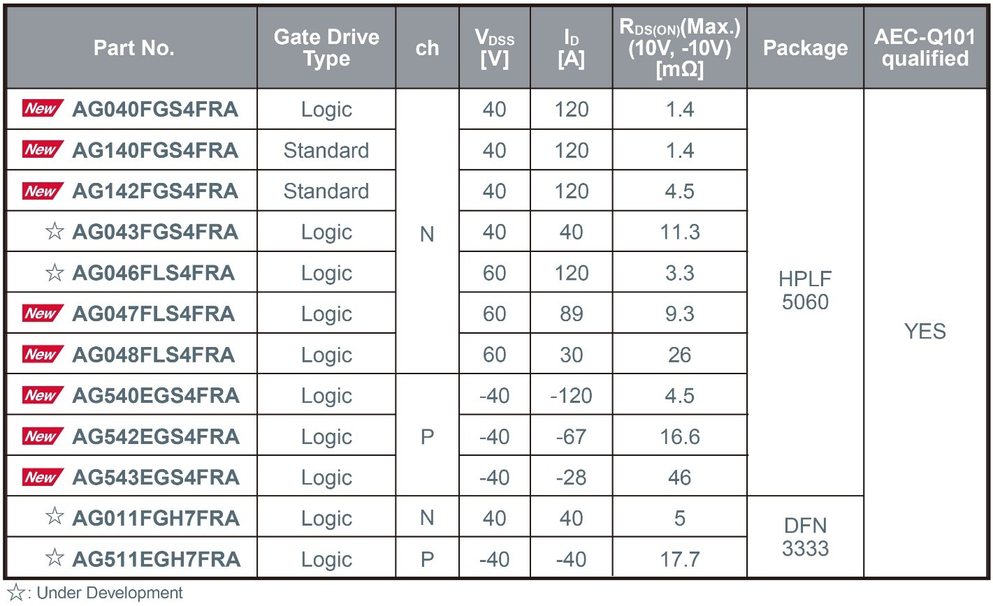
ROHM’s New Compact, Highly Reliable Package Added to Automotive 40V/60V MOSFET Lineup
ROHM has expanded its lineup of low-voltage (40V/60V) MOSFETs for automotive applications – such as main inverter control circuits, electric pumps, and LED headlights – by introducing the latest products adopting the new HPLF5060 package (4.9mm × 6.0mm).
In recent years, automotive low-voltage MOSFETs have been trending toward smaller packages, such as the 5060-size and even more compact options. However, this miniaturisation introduces significant challenges for achieving reliable mounting, primarily due to narrow terminal spacing and leadless designs.
To address these issues, the new HPLF5060 package offers a smaller footprint compared to the widely used TO-252 package (6.6mm × 10.0mm) while enhancing board-mount reliability through the adoption of gull-wing leads. Additionally, the use of copper clip junction technology enables high-current operation, making the HPLF5060 an ideal solution for demanding automotive environments.
Mass production of new products using this package began in November 2025 (sample price: $3.5/unit, excluding tax). Online sales have also started, and the products are also available for online purchase through online distributors such as DigiKey and Farnell.
In addition to expanding the lineup of products using this package, mass production of the smaller DFN3333 (3.3mm × 3.3mm) package, which employs wettable flank technology, is scheduled to begin around February 2026. Furthermore, development has commenced on a TOLG (TO-Leaded with Gull-wing) package (9.9mm × 11.7mm) to further expand the lineup of high-power, high-reliability packages.
The post ROHM’s New Compact, Highly Reliable Package Added to Automotive 40V/60V MOSFET Lineup appeared first on ELE Times.
Fraunhofer ISE achieves record efficiencies for tandem photovoltaic modules
Building I2C-PPS. Part 2 - Planning
 | Continuing from the idea published a couple of days before - Building a programmable DC-DC Power Supply with I2C Interface (I2C-PPS). Part 1 - Idea. I decided to get some intuition about overall device structure before gathering its schematics. As I sketched it in the picture the buck-boost converter can be seen as the set of several blocks - a power stage, input and output filters with respective current sensors, a set of programming resistors, a digital I/O plus indication circuit, and a master switch. The power stage consist of 4 power MOSFETs and the inductor. The input and output filters are sets of capacitors mixed with current sensing resistors. The converter's operation mode and HW limits on voltage and current are set by programming resistors. And digital I/O with indication circuit provides interface for RPI and some leds for us - humans. The master switch makes it possible to start or shutdown the thing as it needed independently by RPI as it's needed. Normally, it should stay off and should go off if RPI goes down turning the converter off when input voltage is here without running RPI. For the switcher TI provides a design calculator in form of an excel spreadsheet and schematic design checklist which allow to select values for main components with desired input and output specs in mind. As for now I decided to go with 4-6V input window but it really should stay at 5V and set HW input and output current limits at 5A. With 250kHz switching frequency many 10uH inductors with Isat > 7A and DCR in recommended range should work along with set of recommended power MOSFETs. More details you can find in the project repo - github.com/condevtion/i2c-pps. Looks like it's time to pull KiCAD into the project. [link] [comments] |
AI in 2026: Enabling smarter, more responsive systems at the edge

As artificial intelligence (AI) continues its momentum across the electronics ecosystem, 2026 is shaping up to be a defining year for edge AI. After years of rapid advancement in cloud‑centric AI training and inference, the industry is reaching a tipping point. High‑performance intelligence is increasingly migrating to the edge of networks and into systems that must operate under stringent constraints on latency, power, connectivity, and cost.
This shift is not incremental. It reflects a broader architectural evolution in how engineers design distributed intelligence into next‑generation products, systems, and infrastructure.
Consider an application such as detecting dangerous arc faults in high‑energy electrical switches, particularly in indoor circuit breakers used in residential, commercial, or industrial environments. The challenge in detecting potential arc faults quickly enough to trip a breaker and prevent a fire hazard is that traditional threshold‑based criteria often generate an impractically high number of false positives, especially in electrically noisy environments.
An AI‑based trigger‑detection approach can significantly reduce false positives while maintaining a low rate of false negatives, delivering a more practical and effective safety system that ultimately saves lives.
What edge AI means for design
Edge AI refers to artificial intelligence processing performed on or near the physical hardware that collects and acts on data, rather than relying solely on remote cloud data centers. By embedding inference closer to where data originates, designers unlock real‑time responsiveness, tighter privacy controls, and reduced dependence on continuous network connectivity.
These capabilities allow systems to make decisions in milliseconds rather than seconds, a requirement across many industrial and embedded domains.

Figure 1 Smart factory environments demand immediate pattern recognition and decision‑making.
From factory automation to safety‑critical monitoring, the need for immediate pattern recognition and decision‑making has become a core design constraint. Systems must be engineered to operate with local intelligence that is context‑aware and resilient, maintaining performance even during intermittent or unavailable cloud connectivity.
Engineering drivers behind the edge shift
Design engineers are responding to several overlapping trends.
- Latency and determinism
Latency remains a fundamental limiter in real‑time systems. When AI models execute at the edge instead of in the cloud, network round‑trip delays are eliminated. For applications such as command recognition, real‑time anomaly detection, and precision control loops, deterministic timing is no longer optional—it is a design requirement.

Figure 2 Latency issues are driving many industrial applications toward edge AI adoption.
In the arc‑fault detection example described earlier, both latency and determinism are clearly essential in a safety‑oriented system. However, similar constraints apply to other domains. Consider an audio‑based human‑machine interface for an assistive robot or a gesture‑based interface at an airport kiosk. If system response is delayed or inconsistent, the user experience quickly degrades. In such cases, local, on‑device inference is critical to product success.
- Power and energy constraints
Embedded platforms frequently operate under strict power and energy constraints. Delivering AI inference within a fixed energy envelope requires careful balancing of compute throughput, algorithm efficiency, and hardware selection. Engineering decisions must support sustained, efficient operation while staying within the electrical and packaging limits common in distributed systems.
- Data privacy and security
Processing AI locally reduces the volume of sensitive information transmitted across networks, addressing significant privacy and security concerns. For systems collecting personal, operational, or safety‑critical data, on‑device inference enables designers to minimize external exposure while still delivering actionable insights.
For example, an occupancy sensor capable of detecting and counting the number of people in hotel rooms, conference spaces, or restaurants could enable valuable operational analytics. However, even the possibility of compromised personal privacy could make such a solution unacceptable. A contained, on‑device system becomes essential to making the application viable.
- Resource efficiency and scalability
In deployments involving thousands or millions of endpoints, the cumulative cost of transmitting raw data to the cloud and performing centralized inference can be substantial. Edge AI mitigates this burden by filtering, transforming, and acting on data locally, transmitting only essential summaries or alerts to centralized systems.
Edge AI applications driving design innovation
Across industries, edge AI is moving beyond pilot programs into full production deployments that are reshaping traditional design workflows.
Industrial systems
Predictive maintenance and anomaly detection now occur directly at the machine, reducing unplanned downtime and enabling real‑time operational adjustments without dependence on remote analytics.

Figure 3 Edge AI facilitates predictive maintenance directly at the machine.
Automotive and transportation
In‑vehicle occupancy sensing is emerging as a critical edge AI application. Systems capable of detecting the presence of passengers—including children left in rear seats—must operate reliably and in real time without dependence on cloud connectivity.
On‑device AI enables continuous monitoring using vision, radar, or acoustic data while preserving privacy and ensuring deterministic system response. These designs prioritize safety, low power consumption, and secure local processing within the vehicle’s embedded architecture.
Consumer and IoT devices
Smart devices that interpret voice, gesture, and environmental context locally deliver seamless user experiences while preserving battery life and privacy.
Infrastructure and energy
Distributed assets in energy grids, utilities, and smart cities leverage local AI to balance loads, detect dangerous arc faults, and optimize performance without saturating communication networks. A common theme emerges across these sectors: the more immediate the required intelligence, the closer the AI must reside to the data source.
Design Considerations for 2026 and beyond
Embedding intelligence at the edge introduces new complexities. Beyond system design and deployment, AI development requires structured data collection and model training as both an initial and ongoing effort. Gathering sufficiently diverse and representative data for effective model training demands careful planning and iterative refinement—processes that differ from traditional embedded development workflows.
However, once structured data collection becomes part of the engineering lifecycle, many organizations find that it leads to more practical, cost‑effective, and impactful solutions.
Beyond data strategy, engineers must address tight memory footprints, heterogeneous compute architectures, and evolving toolchains that bridge model training with efficient, deployable inference implementations. A holistic approach requires profiling real‑world operating conditions, validating model behavior under constraint, and integrating AI workflows with existing embedded software and hardware stacks.
In this context, the selection of compute architecture and development ecosystem becomes critical. Platforms offering a broad performance range, robust security mechanisms, and long product lifecycles enable designers to balance immediate requirements with long‑term roadmap considerations. Integrated development flows that support optimization, profiling, and debugging across the edge continuum further accelerate time to market.
Edge AI in 2026 is not simply a buzz phrase—it’s a strategic design imperative for systems that must act quickly, operate reliably under constraint, and deliver differentiated performance without overburdening networks or centralized infrastructure.
By bringing intelligence closer to where data is generated, engineers are redefining what distributed systems can achieve and establishing a new baseline for responsive, efficient, and secure operation across industries.
Nilam Ruparelia is associate director of Microchip’s Edge AI business unit.
Special Section: AI Design
- The AI design world in 2026: What you need to know
- AI workloads demand smarter SoC interconnect design
- AI’s insatiable appetite for memory
- The AI-tuned DRAM solutions for edge AI workloads
- Designing edge AI for industrial applications
- Round pegs, square holes: Why GPGPUs are an architectural mismatch for modern LLMs
- Bridging the gap: Being an AI developer in a firmware world
- Why power delivery is becoming the limiting factor for AI
- Silicon coupled with open development platforms drives context-aware edge AI
- Designing energy-efficient AI chips: Why power must Be an early design consideration
- Edge AI in a DRAM shortage: Doing more with less
The post AI in 2026: Enabling smarter, more responsive systems at the edge appeared first on EDN.
Сторінки


![[link]](https://i.redd.it/v9veatvgs7kg1.png)