
Збирач потоків
Wireless telemetry on a sub dollar chip!
 | The PIC16F13145 chip is at the center of this, its under a dollar in pretty much every big supplier. For those who dont know, The pic is a little microcontroller, less powerfull than an arduino but what makes it capable of this is that it contains configurable logic blocks. Basically you can reprogram the logic inside of them kind of like in FPGAs. I find it kind of strange how the arduino chips are like 2-3x more expensive while being less capable. This project uses a PIC16f13145 curiosity nano dev board which is a dev board for a configurable logic bloc chip. using no external hardware it transits digital data that can then be picked up and decoded on another radio. For more details visit my post ! How it works: Encoding:The configurable logic uses logic to turn on and off a pin conected to wire which acts as an antenna forming a square wave which causes harmonics allowing us to transmit at 96mhz. This is our carrier. Then we use timers to decide when to turn on or off the the carrier. We use on off keying which means the carrier is either on or off and to increase resilience to timing problems we use manchester encoding. Manchester encoding works by using edges or transitions in aplitude levels to encode 1 and 0. In our case we use the following: bit == 0: outputs 1 then 0 → High to Low → IEEE Manchester 0 bit == 1: outputs 0 then 1 → Low to High → IEEE Manchester 1 In a spectrogram it looks like this: When translated to 1 and 0 to be decoded it looks like the second image We use a sync sequence before each data byte. in this case being 0b11111111. This allows the decoder to understand the timing and synchronise the phase of the manchester encoding. you can see this as the carrier being turned on and off in a repeated pattern before a different pattern in teh spectrogram from gqrx from an rtl sdr. In this example its transmitting 8 bits per second but it could be much faster, this was done so you could see the encoding in the spectrogram. AntennaYou could get real fancy and use a real 100mhz fm antenna but for our case we just need a wire that will radiate the rf carrier. Ideally the wire would be 1/4th the wavelength of the carrier which at around 100mhz is around 75cm but thats relatively long and for short ranges we can afford to make our antenna much smaller even if it costs us signal strength. In my tests i used a 8cm 22awg wire another good thing is that having a short wire will help filter out out of band frequencies such as our original 32mhz signal that creates our 96 mhz harmonic. Though admitedly, at the power level we are transmitting it doesnt matter that much. Decoding and receivingI used an rtl-sdr and I used a python script (main.py) to read samples at 512hz for 8bps and then convert them to digital 1s or 0s which are written to test.txt for me to open on pulseview using the import digital data or binary data option. I can then use the OOK and manchester decoding function that's integrated in pulseview. You could also do this using python directly but then its harder to visualise what's going on. In an earlier commit it did do that though. how to use the code
If you want to change the bitrate you can do so by changing the high and low bytes of the timer defined as 100hz timer even though its only 16hz by default [link] [comments] |
I made a security key with the RP2350!
 | Demo: https://www.youtube.com/watch?v=Fg3U53FJ8HM Hey everyone! I wanted to share MicroKey, a PCB I designed that uses the RP2350 microcontroller and a fork of the Pico Keys software. This setup allows the RP2350 to function as a FIDO WebAuthn security key! I assembled and reflowed this board myself, so please excuse the minor blobs of solder and flux on the otherwise beautiful ENIG finish D: [link] [comments] |
A battery backup for a solar-mains hybrid lamp
 1. The solar-mains hybrid lamp
In the April 4, 2024, issue of EDN, the design of a solar mains hybrid lamp (HL) was featured. The lamp receives power from both a solar panel and a mains power supply to turn on an array of LED lamps. Even when solar power is widely variable, it supplies a constant light output by dynamically drawing balanced power from the mains supply. Also, it tracks the maximum power point very closely.
Wow the engineering world with your unique design: Design Ideas Submission Guide
1.1 AdvantagesThe advantages of the HL are as follows:
- It utilizes all the solar power generated and draws only the necessary power from the grid to maintain constant light output.
- It does not inject power into the grid; hence, it does not contribute to any grid-related issues.
- It uses a localized power flow with short cabling, resulting in negligible transmission losses.
- It uses DC operation, resulting in a simple, reliable, and low-cost system.
- Generated PV power is utilized even if the grid fails, thus acting as an emergency lamp in the event of a grid failure during the daytime.
- It has a lengthy lifespan of 15 years with minimal or no maintenance, resulting in a good return on investment.
The limitations of the HL are as follows:
- It does not provide light if the grid fails after sunset.
- Solar power is not utilized outside of office hours or on holidays.
As mentioned above, the HL’s utility can be fully realized in places such as hospitals, airports, and malls, as it can be used every day of the week.
In offices that are open for work only 5 days per week, the generated PV power will be wasted on weekends and outside of office hours (early mornings and evenings).
For such applications, to fully utilize the generated PV power, a battery backup scheme is proposed. It is designed as an optional add-on feature to the existing HL. The PV power, which would otherwise go to waste, can now be stored in the battery whenever the HL is not in use. The stored energy can be utilized instead of mains power on workdays to reduce the electricity bill. In cases where the grid fails, it will work as an emergency lamp.
2. Battery backup block diagramThe block diagram of the proposed scheme is shown in Figure 1. It consists of a HL having an array of 9 LED lamps, A1 to A9. Each HL has five 1-W white LEDs connected in series, mounted on a metal core PCB (MCPCB). For more details, refer to the previous article, “Solar-mains HL.” Here, the HL is used as is, without any changes.
The PV voltage (Vpv) is supplied through a two-pole two-way switch S1 to the HL. Switch S1A is used to connect the PV panel to either the lamp or to the battery. As shown in the figure, the PV panel is connected to the battery through an Overvoltage Cutoff circuit. This circuit disconnects PV power when the battery voltage reaches its maximum value of Vb(MAX).
A single-pole two-way switch S2 is used to select either MAINS or BAT to feed power to the VM terminal of the HL. When S2 is in the BAT position, battery power is fed through the undervoltage trip circuit. Whenever the battery voltage drops to the minimum value Vb(MIN), the HL is disconnected from the battery. Switch S1B is used to disconnect the battery/mains power to the HL when S1 is in the CHARGE position.
 Figure 1 The proposed add-on battery backup system for HL.
Note: This simple battery cutoff and trip circuit has been implemented to prove the concept of battery backup using the existing HL. In the final design, the Overvoltage Cutoff circuit should be replaced with a solar charge controller, which will track the maximum power point as the battery charges. Readily available off-the-shelf solar charge controllers could be used. The selection of a solar charge controller is given in Section 5.
Here are the lamp specifications:
- Solar PV panel: 30 Wp, Vmp = 17.5 V, Imp = 1.7 A
- Adapter specifications Va = 18 V; Current 2 A
- Lead Acid Battery: 6 V 5 Ah. (3 batteries connected in series)
- Battery nominal voltage Vb = 18V, Vb(MAX) = 19 V, Vb(MIN) = 17 V
- Lamp power output: 30 W
The circuit diagram of the battery Overvoltage Cutoff and Undervoltage Trip is shown in Figure 2. Three lead-acid batteries (6 V, 5 Ah) connected in series are used for storing solar energy. The battery is connected to the solar panel Vpv through a P-channel MOSFET T1 (IRF9540). The Schottky diode D1 (1N5822) is connected in series to prevent the battery from getting discharged into the solar panel when it is not producing any power.
T1 is controlled using comparator CMP1 of IC1 (LM393). The battery voltage is sensed using the potential divider R6 and R7. The reference to the comparator non-inverting pin (3) is generated from a +12-V power supply implemented using the IC2 (LM431) shunt regulator. If the battery voltage is lower than the reference voltage, the CMP1 output (pin 1) is high. This turns on transistor T3, which turns on T1. The green LED_G indicates that the battery is being charged.
 Figure 2 The circuit diagram of Overvoltage Cutoff and Undervoltage Trip circuits.
The battery is connected to the load through MOSFET T2 (IRF9540). T2 is controlled using comparator CMP2 of IC1. The battery voltage is sensed using the potential divider R14 and R15, and is connected to the non-inverting terminal (Pin 5). The reference voltage is connected to the inverting terminal (Pin 6).
So long as the battery voltage is higher than the reference, the CMP2 output remains high. This drives transistor T4, which turns on T2. When the battery voltage drops below the reference, T2 is turned off, thus disconnecting the lamp load. LED_R indicates the battery voltage is within the Vb(MIN) and Vb(MAX) range.
Figure 3 shows the PCB assembled according to the circuit diagram in Figure 2. The connections for the solar panel Vpv, battery Vb, and battery output Vb+ (through the MOSFET T2) are made using three 2-pin screw terminals.

Figure 3: The assembled PCB for battery overvoltage cutoff and undervoltage trip circuit.
Figure 4 shows the interconnections of the battery charger circuit with the HL.
 Figure 4 A top view of the interconnections of the battery charger circuit with the HL.
The modes of operation of this circuit are captured in Table 1. When S1 is in the CHARGE position, the PV voltage is supplied to the batteries for charging. In this mode, the position of S2 does not affect the charging process.
When S1 is in the PV position, the HL turns ON. Using S2 we can select either mains power or battery power.
Table 1 Operating modes of the battery backup circuit: battery charging, hybrid with mains power, and hybrid with battery power.
4. Integration and testingFigure 5 shows the integration of the battery protection circuit with the HL and three batteries. The cable from the PV panel is connected to the 2-pin screw terminal labeled as Vpv. Three 6-V batteries in series are connected to the screw terminal Vb. A DC socket labeled Va is mounted for plugging into the adapter pin. In the photograph, S1 is in CHARGE position, so the battery is being charged using PV power. In this case, the position of S2 is irrelevant and will not affect the charging process.

Figure 5 An image of the circuit in Battery Charging mode. The green LED indicates the battery is being charged from the PV panel. The red LED indicates battery power is available for use.
Figure 6 shows the HL turned on using PV power and a battery. In this case, S1 is in the PV position, and S2 is in the BAT position. Note that the LED lamp array (A1 to A9) is facing downwards. On the HL PCB, there are nine red and nine green indicator LEDs. Each pair of LEDs represents 11% of the total power. The photograph shows four green LEDs are ON, which means 44% of the power is coming from solar. The remaining 55% of power is being drawn from the battery. The green and red LED combination changes as the sunlight varies.
 Figure 6 The lamp in Hybrid mode. Four green LEDs indicate 44% of the power is coming from the PV panel. Five red LEDs indicate 55% of the power is being drawn from the battery.
Here, the design of a 90-W HL with a battery backup is proposed. The nominal working voltage selected is 48 V.
5.1 HL specsThe specifications for the HL design are as follows:
- Solar Panel Specifications: Power = 30 Wp, Vmp = 17.5 V, Imp = 1.7 A
- Number of Solar Panels connected in series: 3
- Solar Array Voltage: Vpv = 3 x 17.5 = 52.5 V; Voc = 60 V
- Number of LEDs in each MCPCB (A1 to A9): 15 white LEDs of 1 Watt each.
- Forward voltage of LED: 3.12 V
- Voltage across each lamp (A1 to A9): 15 x 3.12 = 46.8 V
- Current through LED lamps: 0.2 A (selected)
- Current limiting resistor [1]: R1 to R9 = (52.5 – 46.8)/0.2 = 28.5 Ω (select 27Ω/2W)
- Adapter specifications: 48 V, 2 A
As stated earlier, this lamp can be used without a battery backup in facilities that are open all seven days a week. In these applications, the solar power generated is fully utilized, so the cost of this lamp is minimal. The deployment of a large number of such lamps can significantly reduce the electricity bill.
However, in offices that operate 5 days a week, the power generated during weekends goes to waste. In cases where another load can utilize the available PV power on weekends, such as a pump, vacuum cleaner, or a battery that needs charging, the PV panel’s output can be connected to that load. This way, we can still use the HL as is. However, if there is no other load that can utilize the PV power, then we must resort to battery backup.
5.2 Battery selectionThe battery selection can be as follows:
- Lithium-ion Battery: 13S (13 cells in series), Nominal voltage 48 V
- Battery voltages: Vb(MIN) = 42 V, Vb = 46.8 V, Vb(MAX) = 54.6 V
- Energy storage capacity (24 Ah): 48 x 24 = 1152 Wh
- Solar energy generation per day: 90 W x 6 hrs = 540 Wh
- Battery storage: 1152 Wh / 540 Wh = 2.1 or 2 days
A wide range of solar charge controllers is available on the market. To select a suitable charge controller, the following specifications are provided as guidelines:
- Battery Type: Li-ion, Life-Po4
- Nominal Voltage: 48 V
- Controller type: MPPT
- Maximum output current: 5 A
- Protections: Battery reverse polarity, solar panel reversal, short circuit protection, battery overvoltage cutoff, battery low voltage trip.
Note that the open-circuit voltage (Voc) of the solar array is 60 V; therefore, the selected components should have a voltage rating greater than 60 V.
This design is for a 90-W HL; however, higher-wattage lamps can also be designed. In that case, the lamp MCPCB selected should have a higher power rating. Alternately, the number of MCPCBs can be increased to around 16. This way, the array can be arranged in a 4×4 layout. With an increased number of arrays, both the hardware and software of HL have to be upgraded.
It may be possible to connect two MCPCBs in parallel to increase the lamp power. However, in this case, the two MCPCBs should have a matching LED array forward voltage. This will ensure equal division of lamp current.
5.4 SchedulingThe design shown here uses manual switches which can be replaced with semiconductor switches. In this case, the operation of the HL can be automated with a weekly programming cycle. On weekdays, it will work in hybrid mode. In this mode we can either select mains power or battery power. The duration of battery power consumption can be planned to ensure that battery is available for charging during weekends.
6. Storing the HL’s excess energyThe solar-mains HL proposed earlier, provides constant light irrespective of the sunlight conditions. It is a very cost-effective design and can be deployed in large numbers to reduce electricity costs. However, if it is not used on all 7 days of the week, then the solar power gets wasted. To avoid any power wastage, a battery backup system has been proposed here as an add-on feature. Using batteries, the excess solar energy can be stored. The battery backup makes this lamp work as an emergency lamp, also during grid failures.
Vijay Deshpande recently retired after a 30-year career focused on power electronics and DSP projects, and now works mainly on solar PV systems.
Related Content
- Solar-mains hybrid lamp
- Solar day lamp designs use passive and active current limiting circuits
- Solar day lamp designs provide low-cost lighting solutions, Part 1
- Solar day lamp designs provide low-cost lighting solutions, Part 2
The post A battery backup for a solar-mains hybrid lamp appeared first on EDN.
How to prevent overvoltage conditions during prototyping

The good thing about being a field applications engineer is that you get to work on many different circuits, often all at the same time. While this is interesting, it also presents problems. Jumping from one circuit to another involves disconnecting a spaghetti of leads and probes, and the chance for something going wrong increases exponentially with the number of wires involved.
It’s often the most basic things that are overlooked. While the probes and leads are checked and double checked to ensure everything is in place, if the voltage on the bench power supply is not adjusted correctly, the damage can be catastrophic, causing hours of rework.
The circuit described in this article helps save the day. Being a field applications engineer also results in a myriad of evaluation boards being collected, each in a state of modification, some of which can be repurposed for personal use. This circuit is based on an overvoltage/reverse voltage protection component, designed to protect downstream electronics from incorrect voltages being applied in automotive circuits.
Such events are caused by the automotive battery being connected the wrong way or a load dump event where the alternator becomes disconnected from the battery, causing a rise in voltage applied to the electronics.
Circuit’s design details
As shown in Figure 1, MAX16126 is a load dump protection controller designed to protect downstream electronics from over-/reverse-voltage faults in automotive circuits. It has an internal charge pump that drives two back-to-back N-channel MOSFETs to provide a low loss forward path if the input voltage is within a certain range, configured using external resistors. If the input voltage goes too high or too low, the drive to the gates of the MOSFETs is removed and the path is blocked, collapsing the supply to the load.

Figure 1 This is how over-/reverse-voltage protection circuit works. Source: Analog Devices Inc.
MAX16127 is similar to MAX16126, but in the case of an overvoltage, it oscillates the MOSFETs to maintain the voltage across the load. If a reverse voltage occurs on the input, an internal 1 MΩ between the GATE and SRC pins of the MAX16126 ensures MOSFETs Q1 and Q2 are held off, so the negative voltage does not reach the output. The MOSFETs are connected in opposing orientations to ensure the body diodes don’t conduct current.
The undervoltage pin, UVSET, is used to configure the minimum trip threshold of the circuit while the overvoltage pin, OVSET, is used to configure the maximum trip threshold. There is also a TERM pin connected via an internal switch to the input pin and this switch is open circuited when the part is in shutdown, so the resistive divider networks on the UVSET and OVSET pins don’t load the input voltage.
In this design, the UVSET pin is tied to the TERM pin, so the MOSFETs are turned on when the device reaches its minimum operating voltage of 3 V. The OVSET pin is connected to a potentiometer, which is adjusted to change the overvoltage trip threshold of the circuit.
To set the trip threshold to the maximum voltage, the potentiometer needs to be adjusted to its minimum value and likewise for the minimum trip threshold the potentiometer is at its maximum value. The IC switches off the MOSFETs when the OVSET pin rises above 1.225 V.
The overvoltage clamping range should be limited to between 5 V and 30 V, so resistors are inserted above and below the potentiometer to set the upper and lower thresholds. There are Zener diodes connected across the UVSET and OVSET pins to limit the voltage of these pins to less than 5.1 V.
Assuming a 47-kΩ resistor is used, the upper and lower resistor values of Figure 1 can be calculated.
To achieve a trip threshold of 30 V, Equation 1 is used:
![]()
To achieve a trip threshold of 5 V, Equation 2 is used:
![]()
Equating the previous equations gives Equation 3:
![]()
So,
![]()
From this,
![]()
Using preferred values, let R3 = 10 kΩ and R2 = 180 kΩ. This gives an upper limit of 29 V and a lower limit of 5.09 V. This is perfect for a 30 V bench power supply.
Circuit testing
Figure 2 shows the prototype PCB. The trip threshold voltage was adjusted to 12 V and the circuit was tested.

Figure 2 Modified evaluation kit illustrate the circuit testing. Source: Analog Devices Inc.
The lower threshold was measured at 5.06 V and the upper threshold was measured at 28.5 V. With a 10-V input and a 1-A load, the voltage measured between input and output was measured at 19 mV, which aligns with the MOSFET datasheet ON resistance of about 10 mΩ.
Figure 3 shows the response of the circuit when a 10-V step was applied. The yellow trace is the input voltage, and the blue trace shows the output voltage. The trip threshold was set to 12 V, so the input voltage is passed through to the output with very little voltage drop.

Figure 3 A 10-V step is applied to the input of MAX16126. Source: Analog Devices Inc.
The input voltage was increased to 15 V and retested. Figure 4 shows that the output voltage stays at 0 V.

Figure 4 A 15-V step is applied to the input of MAX16126. Source: Analog Devices Inc.
The input voltage was reversed, and a –7 V step was applied to the input, with the results shown in Figure 5.

Figure 5 A –7 V step is applied to the input of MAX16126. Source: Analog Devices Inc.
The negative input voltage was increased to –15 V and reapplied to the input of the circuit. The results are shown in Figure 6.

Figure 6 A –15 V step is applied to the input of MAX16126. Source: Analog Devices Inc.
Caution should be exercised when probing the gate pins of the MOSFETs when the input is taken to a negative voltage. Referring to Figure 1, the body diode of Q1 pulls the two source pins toward VIN, which is at a negative voltage. There is an internal 1 MΩ resistor between the GATE and SRC connections of MAX16126, so when a ground referenced 1 MΩ oscilloscope probe is attached to the gate pins of the MOSFETs, the oscilloscope probe acts like a 1 MΩ pull-up resistor to 0 V.
As the input is pulled negative, a resistive divider is formed between 0 V, the gate voltage, and the source of Q2, which is being pulled negative by the body diode of Q1. When the input voltage is pulled to lower than twice the turn-on voltage of Q2, this MOSFET turns on and the output starts to go negative. Using a higher impedance oscilloscope probe overcomes this problem.
A simple modification to the MAX16126 evaluation kit provides reassuring protection from user-generated load dump events caused by momentary lapses in concentration when testing circuits on the bench. If the components in the evaluation kit are used, the circuit presents a low loss protection circuit that is rated to 90 V with load currents up to 50 A.
Simon Bramble specializes in analog electronics and power. He has spent his career in analog electronics and worked at Maxim and Linear Technology, both now part of Analog Devices Inc.
Related Content
- OverVoltage Protection Circuit
- Pressures grow for circuit protection
- Overvoltage-protection circuit saves the day
- Overvoltage protection for sensitive amplifier applications
- Provide robust input overvoltage protection for amplifier analog input modules
The post How to prevent overvoltage conditions during prototyping appeared first on EDN.
AEK-MOT: 2 new challenges facing motor control applications in cars and what we are doing to address them
By: STMicroelectronics
Over the years, ST has multiplied the AutoDevKit development boards for motor control applications in cars, which all have a name that starts with “AEK-MOT”. There are general systems like the AEK-MOT-2DC40Y1 for driving three DC motors, the AEK-MOT-3P99081 for brushless motors, and the AEK-MOT-SM81M1 for stepper motors. There are also more targeted approaches like the AEK-MOT-TK200G1 for powered liftgates or the AEK-MOT-WINH92 for powered windows. The reason behind this broad range of solutions is that engineering needs in cars are changing, and as applications become varied, so must the solutions that address them. Let’s explore how those who make cars are looking at them differently.
How the car has changed Challenge 1: Application diversification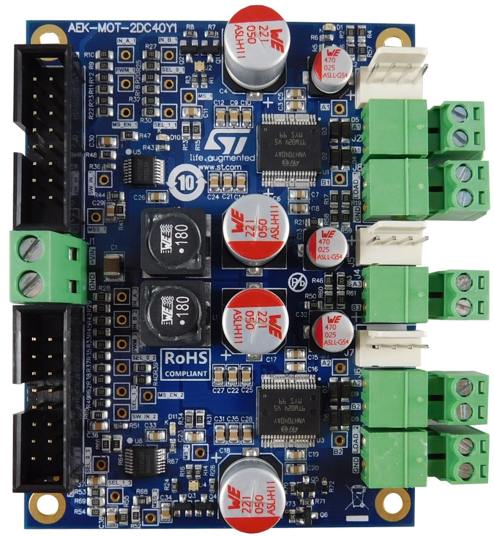 The AEK-MOT-2DC40Y1
While many talk about the electrification of cars or the advent of AI in vehicles, there’s one trend that many overlook. In a span of a couple of decades, vehicles went from having about ten or so motor control applications to close to 50, and we are going to reach a hundred in a few years. The reason is simple: as cars become more digital, replacing a basic mechanical system with a motor control application means greater safety and the ability to add smart features. There are popular examples, such as powered windows, doors, or trunks. There are also systems that many drivers are oblivious to, like active suspensions, electric braking and power steering, EV drivetrains, new actuators, and more.
Challenge 2: Architectural transformationMoreover, the underlying foundation of the car itself is going through a major shift as many adopt a zonal architecture. In essence, it means that engineers organize electric control units based on their zone or physical location instead of just grouping similar features together. It has the advantage of simplifying designs. In some cases, moving to a zonal architecture helped reduce the overall harness weight by 20%. It also means that engineers can use much more powerful computing systems, leading engineers to use an even more diverse range of motor control applications as they infuse artificial intelligence in more parts of the car.
The need for new motor control applications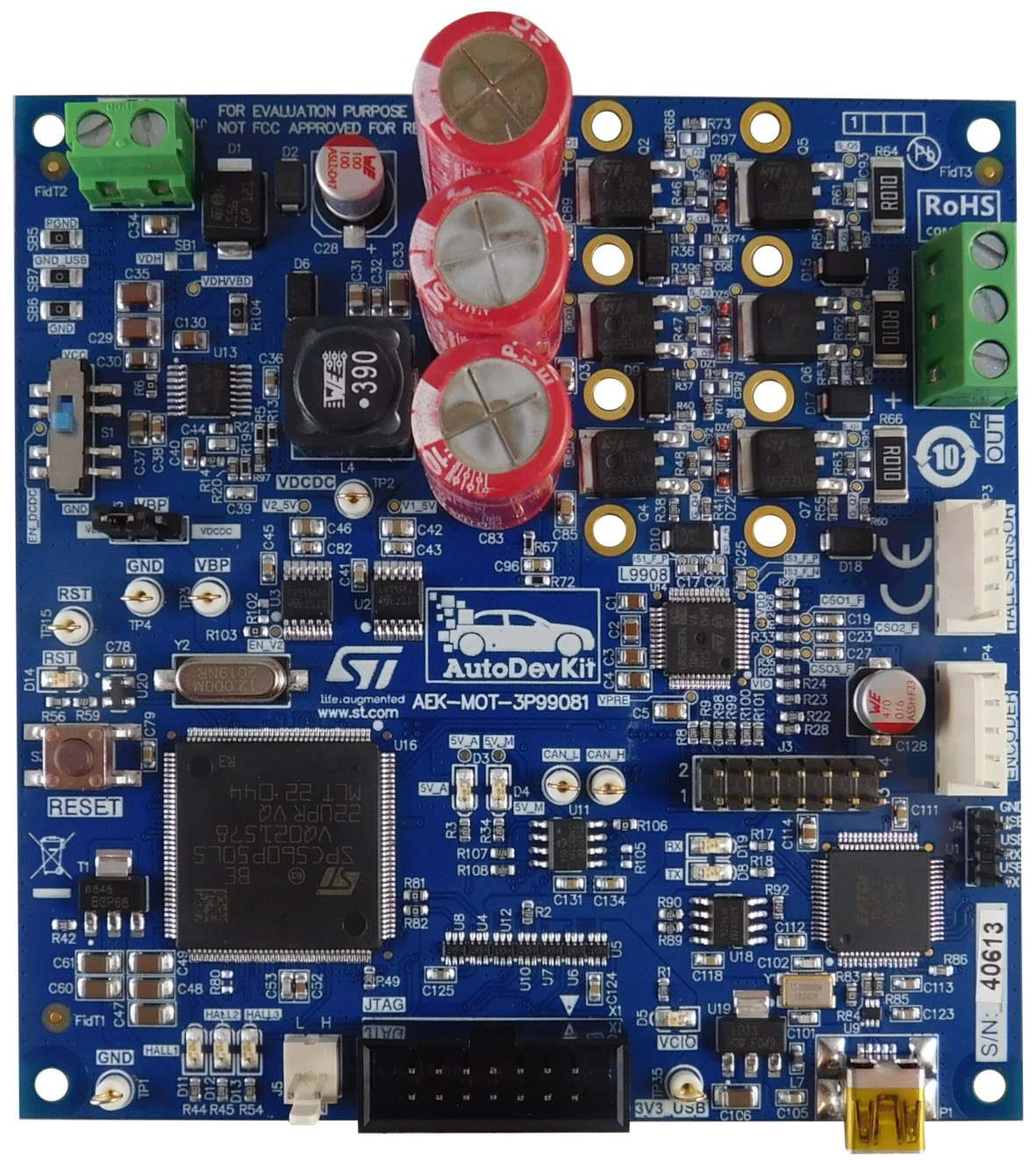 The AEK-MOT-3P99081
This trend comes with two significant challenges. The first one is that as more diverse applications use motor control systems, OEMs need different motor drivers and motor types. Some also wonder whether they need an integrated or non-integrated solution. Simply put, as the kinds of applications become more varied, teams struggle to find new solutions to meet their needs. The second challenge is that designers are looking at cars differently. The move to zonal architectures means that more diverse systems must easily interact with one another. Put simply, teams are increasingly looking at the vehicle as a whole rather than the sum of its parts, and they need solutions that can meet this new global vision.
AEK-MOT or how to keep up with the changes A comprehensive ecosystemAnother challenge is that each automated component must talk to the central unit, which means dealing with numerous interfaces. Currently, some systems prioritize SPI, while others use LIN, CAN, 100BASE-TX, 10BASE-T1S, or something else entirely. As engineers look at the car more globally, they are demanding motor control systems that can work with both new and existing interfaces. How a motor control application implements these systems also matters. Are they integrated or not? Does the SDK make one more accessible than the others, and can abstraction layers help solve these issues? This is why our AutoDevKit ecosystem includes varied development boards and a software library to take advantage of them more easily.
Furthermore, to enhance the transition towards software-defined vehicles (SDV), ST has developed an additional AutoDevKit functional block, AEK-COM-10BASET, that acts as a gateway between the legacy protocols found in most motor driver ICs and the new trendy 10BASE-T1S. The latter is a key building block for the new Remote Control Protocol (RCP) specification currently in progress (Open Alliance – TC18 Remote Control Protocol), which uses native Ethernet frames on 10BASES-T1S for deterministic performance. In essence, RCP is an intermediary between the Ethernet physical interface and SPI or I2C to access registers or talk to the microcontroller.
Non-integrated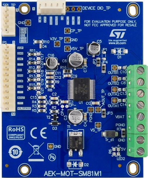 The AEK-MOT-SM81M1
The AEK-MOT-2DC40Y1 can drive up to three DC motors, two bi-directional in parallel or three with proper sequencing. It features VN7 high-side switches and the VNH704AY integrated H-bridge motor driver. The documentation shows how to set up the motors and the configurations available. Additionally, developers can use the graphical user interface in AutoDevKit to manage rotation direction, start them, increase or decrease their speed, and more. The AEK-MOT-2DC40Y1 connects to an SPC5 MCU board, meaning integrators can rapidly design a proof-of-concept. Similarly, the AEK-MOT-SM81M1 also connects to an SPC5 board but features the L99SM81V stepper motor driver, while the AEK-MOT-WINH92 for window lifts uses the L99H92.
IntegratedThe AEK-MOT-3P99081 focuses on CAN-controlled brushless motors. It is an integrated solution with an SPC560P microcontroller and the L9908 gate driver. The MCU talks with the driver through an SPI interface for easy access to configuration options, protection features, and diagnostic messages. Similarly, the AEK-MOT-TK200G1 for powered liftgate runs on the SPC582B60E1 microcontroller and the L99DZ200G drivers, which supports LIN and HS-CAN interfaces for MCU programming during production. Developers talk to the board using a CAN bus to make it easier to access the motor remotely, meaning from another domain controller. Avid readers will remember it was at the center of our AEKD-TRUNKL1 demo.
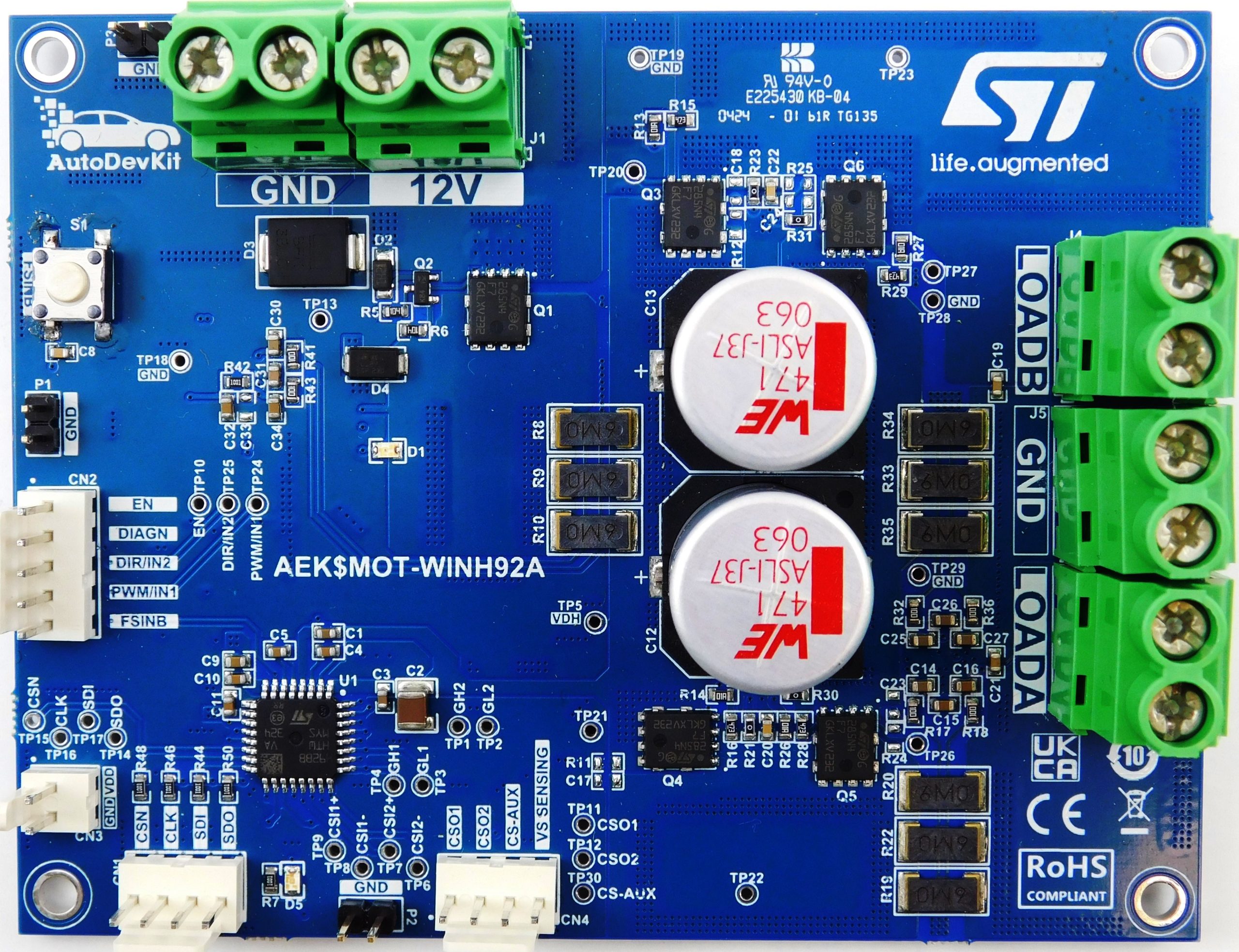 The AEK-MOT-WINH92
All in all, the comprehensive aspect of the AutoDevKit ecosystem means that the learning curve gets easier as teams use different AEK-MOT development boards. They get a range of integrated and non-integrated solutions that all work together under one ecosystem. As a result, everyone, from the decision-makers to the engineers building the platform, can more easily look at the car as a whole and see how all its components can come together under one overarching system. This means that ST is uniquely positioned to become a one-stop shop as more and more motor control applications transform vehicles.
The post AEK-MOT: 2 new challenges facing motor control applications in cars and what we are doing to address them appeared first on ELE Times.
STMicroelectronics and Metalenz Sign a New License Agreement to Accelerate Metasurface Optics Adoption
- New license agreement enabling the proliferation of metasurface optics across high-volume consumer, automotive and industrial markets: from smartphone applications like biometrics, LIDAR and camera assist, to robotics, gesture recognition, or object detection.
- The agreement broadens ST’s capability to use Metalenz IP to produce advanced metasurface optics while leveraging ST’s unique technology and manufacturing platform combining 300mm semiconductor and optics production, test and qualification.
STMicroelectronics, a global semiconductor leader serving customers across the spectrum of electronics applications and Metalenz, the pioneer of metasurface optics, announced a new license agreement. The agreement broadens ST’s capability to use Metalenz IP to produce advanced metasurface optics while leveraging ST’s unique technology and manufacturing platform combining 300mm semiconductor and optics production, test and qualification.
“STMicroelectronics is the unique supplier on the market offering a groundbreaking combination of optics and semiconductor technology. Since 2022, we have shipped well over 140 million metasurface optics and FlightSense modules using Metalenz IP. The new license agreement with Metalenz bolsters our technology leadership in consumer, industrial and automotive segments, and will enable new opportunities from smartphone applications like biometrics, LIDAR and camera assist, to robotics, gesture recognition, or object detection,” underlined Alexandre Balmefrezol, Executive Vice President and General Manager of STMicroelectronics’s Imaging Sub-Group. “Our unique model, processing optical technology in our 300mm semiconductor fab, ensures high precision, cost-effectiveness, and scalability to meet the requests of our customers for high-volume, complex applications.”
“Our agreement with STMicroelectronics has the potential to further fast-track the adoption of metasurfaces from their origins at Harvard to adoption by market leading consumer electronics companies,” said Rob Devlin, co-founder and CEO of Metalenz. “By enabling the shift of optics production into semiconductor manufacturing, this agreement has the possibility to further redefine the sensing ecosystem. As use cases for 3D sensing continue to expand, ST’s technology leadership in the market together with our IP leadership solidifies ST and Metalenz as the dominant forces in the emergent metasurface market we created.”
The new license agreement aims to address the growing market opportunity for metasurface optics projected to experience significant growth to reach $2B by 2029*; largely driven by the industry’s role in emerging display and imaging applications. (*Yole Group, Optical Metasurfaces, 2024 report)
The post STMicroelectronics and Metalenz Sign a New License Agreement to Accelerate Metasurface Optics Adoption appeared first on ELE Times.
Altum RF announces sales representative agreement with RF Alliance
A Strange Diode Burnout Issue in a High-Voltage Medical TX Board — Lessons Learned
 | Hi everyone, This is a TX board for a high-voltage medical controller. The PCB includes:
We're now optimizing the design and replacing the layout, but we hope this case provides some insights to those troubleshooting strange diode failures in high-voltage systems. [link] [comments] |
BLACKBOX AI: Dissecting the AI Network Traffic
Courtesy: Keysight Technologies
Blackbox AI is an AI-powered coding assistant designed to enhance developer productivity by offering features such as code generation, code search, and code completion across multiple programming languages. It integrates seamlessly with popular development environments like Visual Studio Code and provides tools for tasks including autocompletion, natural language to code conversion, and code extraction from various sources.
The platform employs a multi-model architecture, integrating several advanced large language models (LLMs) to deliver comprehensive coding assistance. These include GPT-4o, Claude 3.5 Sonnet, Gemini Pro, LLaMA 3.1, DeepSeek R1 and more .
The ATI team in Keysight has analyzed the network traffic of Blackbox AI and found some interesting insights, which can be helpful for other researchers, optimize performance and ensure secure usage. This was done utilzing a HAR captures of a web session. Blackbox AI operates with standard web protocols, relying on secure TLS encryption for communication.
Overall AnalysisWe have performed extensive user interactions with the Blackbox AI web application. The captured traffic was completely TLS encrypted. We have further analyzed the traffic based on host names.

In the figure above we can observe the maximum number of request-response was seen by www.blackbox.ai followed by www.useblackbox.io. The first host has been observed as the main host responsible for handling core dynamic functionalities such as user authentication and session management. While the latter is for telemetry and analytics, logging events, and user interactions.
 Figure 2: Cumulative payload per host
The diagram above shows that the host www.blackbox.ai has the maximum cumulative payload followed by api-iam.intercom.io. The rest of the hosts are creating smaller network footprints.
Analyzing EndpointsBy examining the HAR file, we gain a detailed view of the HTTP requests and responses between the client and Blackbox AI’s servers. This analysis focuses on critical endpoints and their roles in the platform’s functionality.
Session AuthenticationEndpoint: /api/auth/session
- Method: GET

- Purpose: Checks or retrieves the current user session and related authentication status.
- Request Headers:
- Accept: application/json
- Content-Type: application/json
- Origin: https://www.blackbox.ai (Ensures requests originate from BlackBox AI’s platform)
- Response Status: 200 OK (active session or session data returned)
- Response Body: JSON object containing user session status, expiry, and authentication details
This endpoint is essential for maintaining secure access to Blackbox AI, allowing the platform to verify and manage user sessions and authentication status.
Query ExecutionEndpoint: /api/chat
- Method: POST

- Purpose: Processes user queries and returns AI-generated responses.
- Request Headers:
- Content-Type: application/json
- Accept: application/json
- Origin: https://www.blackbox.ai (Ensures requests originate from BlackBox AI’s platform)
- Request Payload: JSON object with the user’s query and session details.
- Response Status: 200 OK (successful query processing)
This endpoint is central to Blackbox AI’s functionality, enabling dynamic interactions between users and the AI model.
Source VerificationEndpoint: /api/check-sources
- Method: POST

- Purpose: Validates the origin of the provided input or context for generating responses or citations.
Request Headers: - Content-Type: application/json
- Accept: application/json
- Origin: https://www.blackbox.ai (Ensures requests originate from BlackBox AI’s platform)
- Request Payload: Contains the query type and the user’s input
- Response Status: 200 OK (source check completed)
- Response Body: JSON object with source metadata or validation results
This endpoint ensures the integrity of AI responses by validating the origin and credibility of the user’s input, reinforcing trust in generated outputs.
Telemetry LoggingEndpoint: /tlm
- Method: POST

- Purpose: Logs user behavior or system diagnostics to help improve product performance and stability.
Request Headers: - Content-Type: application/json
- Accept: */*
- Origin: https://www.blackbox.ai (Ensures requests originate from BlackBox AI’s platform)
- Request Payload: The request payload contains a JSON object logging a user event with its type, timestamp, and specific details like the action performed and its duration.
- Response Status: 200 OK (telemetry event accepted)
- Response Body: Confirmation message or status log
This endpoint supports platform reliability and user experience optimization by capturing detailed telemetry data on user behavior and system performance.
NOTE: While BLACKBOX AI can be useful, it is a prohibited tool by many companies and government entities. Policy and technical systems must be in place to prevent usage, and it is vital to confirm this via test using BreakingPoint. These tests help validate the security measures and help organizations prevent accidental or malicious use of the platform.
Blackbox AI Traffic Simulation in Keysight ATIAt Keysight Technologies Application and Threat Intelligence (ATI), since we always try to deliver the hot trending application, we have published the network traffic related to Blackbox AI in ATI-2025-07 StrikePack which simulates the HAR collected from the Blackbox AI web application as of April 2025 including different user actions like performing text-based queries, uploading multimedia files, refining search results, managing saved searches. Here all the HTTP transactions are replayed in HTTP/2 over TLS1.3.
 Figure 3: Blackbox AI Apr25 HAR Replay HTTP/2 over TLS1.3 Superflow in BPS
The Blackbox AI application and its 4 new Superflows as shown below:
 Figure 4: Blackbox AI App and its Superflows in BPS
Keysight’s Application and Threat Intelligence subscription provides daily malware and bi-weekly updates of the latest application protocols and vulnerabilities for use with Keysight test platforms. The ATI Research Centre continuously monitors threats as they appear in the wild. Customers of BreakingPoint now have access to attack campaigns for different advanced persistent threats, allowing BreakingPoint Customers to test their currently deployed security control’s ability to detect or block such attacks.

Sulagna Adhikary (R&D at Keysight ATI)
The post BLACKBOX AI: Dissecting the AI Network Traffic appeared first on ELE Times.
HENXV Announces Latest Range of Innovative Power and Communication Products
HENXV announced its latest range of innovative products designed to elevate system performance and reliability: AC/DC Converters, DC/DC Converters, and Bus Transceiver Modules.
New Products:
1. AC/DC Converters: It delivers stable power conversion with high efficiency, compact designs, and robust safety features, ideal for Industrial Automation, Medical, IoT, Electric Vehicles, and many more.
2. DC/DC Converters: Offering precise voltage regulation and high power density, these converters are built to support demanding applications, ensuring reliable performance in telecommunications, automotive, renewable energy, and many more.
3. Bus Transceiver Modules: Designed for seamless data communication, these transceiver modules provide high-speed, low-latency performance with compatibility across industry-standard protocols, perfect for IoT devices, industrial networks, etc.
Why Choose HENXV?
Reliability and Quality: Rigorously tested to ensure durability and consistent performance.
Customizable Solutions: Tailored options to meet specific project requirements.
Dedicated Support: A team to provide technical assistance and ensure smooth integration.
Warranty: 3 years of warranty on all products.
Certifications: All products certified with CE, ROHS, and REACH.
The post HENXV Announces Latest Range of Innovative Power and Communication Products appeared first on ELE Times.
Rohde & Schwarz verifies Next Generation eCall for EN 17240:2024 Standard
Introduced in 2015, eCall, an automated vehicle emergency call system, has been a mandatory requirement for all new cars sold within the European Union since 2018. However, as 2G/3G circuit-switched cellular networks become obsolete, emergency call systems will need to be adapted to 4G/5G packet-switched cellular networks. The European Commission has defined in its most recent regulation that NG eCall will be obligatory starting January 1, 2026. This standard establishes guidelines for testing eCall systems over IP Multimedia Subsystem (IMS) networks, including advanced 4G LTE and 5G NR technologies. Consequently, to incorporate the new NG eCall features in eCall modules, the automotive industry will require NG eCall testing solutions.
The Snapdragon Auto 5G Modem-RF is a 5G automotive-grade platform that has paved the way for next-generation connected vehicles, delivering high-speed connectivity, advanced positioning, and support for Vehicle-to-Everything (V2X) technology. Designed to meet the demands of modern telematics, it supports reliable connectivity, precise multi-band GNSS navigation, and enhanced safety.
Through this joint effort, Rohde & Schwarz and Qualcomm Technologies have successfully verified the compliance of the Snapdragon Auto 5G Modem-RF’s NG eCall functionality with the most recent eCall standards. The verification process employed the Rohde & Schwarz CMX500 mobile radio tester, a comprehensive testing solution for NG eCall including voice and data transmission. This rigorous test, which was simulating a Public Safety Answering Point (PSAP), validated the compliance of the implementation at both ends with the EN 17240:2024 standard. Moreover, the CMX500 supports both 4G and 5G technologies, aiming to provide that the solutions are future-proof.
“We are pleased to have joined forces with Qualcomm Technologies on the verification of their chipsets’ NG eCall implementation,” said Juergen Meyer, Vice President Market Segment Automotive at Rohde & Schwarz. “This collaboration sets a new benchmark for the future of emergency call services, providing the automotive industry a robust and dependable solution to meet the latest eCall standards.”
As a highly versatile tool, the CMX500 with the CMX-KA098 software option can be effectively used for NG eCall testing under realistic network conditions.
The post Rohde & Schwarz verifies Next Generation eCall for EN 17240:2024 Standard appeared first on ELE Times.
Dad and I fabricated IR LED chips from our garage
 | My immigrant dad has been working on his IR LED chip fab setup in our garage, and finally produced some [link] [comments] |
Fixing bent pins
 | I know it won't reflect the light like a brand new one does, but getting all the pins lined up is awesome [link] [comments] |
Firmware-upgrade functional defection and resurrection

My first job out of college was with Intel, in the company’s nonvolatile memory division. After an initial couple of years dabbling with specialty EPROMs, I was the first member from that group to move over to the then-embryonic flash memory team to launch the company’s first BootBlock storage device, the 28F001BX. Your part number decode is correct: it was a whopping 1 Mbit (not Gbit!) in capacity  . Its then-uniqueness derived from two primary factors:
- Two separately erasable blocks, asymmetrical in size
- One of which (the smaller block) was hardware-lockable to prevent unintentional alteration of its contents, perhaps obviously to allow for graceful recovery in case the main (larger) block’s contents, the bulk of system firmware, somehow got corrupted.
The 28F001BX single-handedly (in admitted coordination with Intel’s motherboard group, the first to adopt it) kickstarted the concept of upgradable BIOS for computers already in the field. Its larger-capacity successors did the same thing for digital cellular phones, although by then I was off working on even larger capacity devices with even more (symmetrical, this time) erase blocks for solid-state storage subsystems…which we now refer to as SSDs, USB flash sticks, and the like. This all may explain why in-system firmware updates (which involve much larger code payloads nowadays, of course)—both capabilities and pitfalls—have long been of interest to me.
The concept got personal not too long ago. Hopefully, at least some of you have by now read the previous post in my ongoing EcoFlow portable power station (and peripheral) series, which covered the supplemental Smart Extra Battery I’d gotten for my DELTA 2 main unit:

Here’s what they look like stacked, with the smart extra battery on top and the XT150 cable interconnecting them, admittedly unkempt:

Although that earlier writeup was published on April 23, I’d actually submitted it on March 11. A bit more than a week post-submission, the DELTA 2 locked up. A week (and a day) after the earlier writeup appeared at EDN.com, I succeeded in bringing it back to life (also the day before my birthday, ironically). And in between those two points in time, a surrogate system also entered my life. The paragraphs that follow will delve into more detail on all these topics, including the role that firmware updates played at both the tale’s beginning and end points.
A locked-up DELTA 2To start, let’s rewind to mid-March. For about a week, every time I went into the furnace room where the gear was stored, I’d hear the fan running on the DELTA 2. This wasn’t necessarily atypical; every time the device fired up its recharge circuits to top off the battery, the fan would briefly go on. And everything looked normal remotely, through the app:

But eventually, the fan-running repetition, seemingly more than mere coincidence, captured my attention, and I punched the DELTA 2’s front panel power button to see what was going on. What I found was deeply disturbing. For one thing, the smart extra battery was no longer showing as recognized by the main unit, even though it was still connected. And more troubling, in contrast to what the app was telling me, the display indicated the battery pack was drained. Not to mention the bright red indicator, suggestive that the battery pack was actually dead:

So, I tried turning the DELTA 2 off, which led to my next bout of woe. It wouldn’t shut down, no matter how long I held the power button. I tried unplugging it, no luck. It kept going. And going. I realized that I was going to need to leave it unplugged with the fan whining away, while in parallel I reached out to customer support, until the battery drained (the zeroed-out integrated display info was obviously incorrect, but I had no idea whether the “full” report from the app was right, either). Three days later, it was still going. I eventually plugged an illuminated workbench light to one of its AC outlets, whose incremental current draw finally did the trick.
I tried plugging the DELTA 2 back in. It turned on but wouldn’t recharge. It also still ignored subsequent manual power-down attempts, requiring that I again drain the battery to force a shutoff. And although it now correctly reported a zeroed battery charge status, the dead-battery icon was now joined by another error message, this indicating overload of device output(s) (?):

At this point, I paused and pondered what might have gone wrong. I’d owned the DELTA 2 for about six months at that point, and I’d periodically installed firmware updates to it via the app running on my phone (and in response to new-firmware-available notices displayed in that app) with no issues. But I’d only recently added the Smart Extra Battery to the mix. Something amiss about the most recent firmware rev apparently didn’t like the peripheral’s presence, I guessed:

So, while I was waiting for customer service to respond, I hit up Reddit. And lo and behold, I found that others had experienced the exact same issue:
ResuscitationIt turns out that V1.0.1.182 wasn’t the most recent firmware rev available, but for reasons that to this day escape me (but seem to be longstanding company practice), EcoFlow didn’t make the V1.0.1.183 successor generally available. Instead, I needed to file a ticket with technical support, providing my EcoFlow account info and my unit’s serial number, along with a description of the issue I was having, and requesting that they “push” the new version to me through the app. I did so, and with less than 24 hours of turnaround, they did so as well:

 Fingers crossed, I initiated the update to the main unit:

Which succeeded:

Unfortunately, for unknown reasons, the subsequent firmware update attempt on the smart extra battery failed, rendering it inaccessible (only temporarily, thankfully, it turned out):


And even on the base unit, I still wasn’t done. Although it was now once again responding normally to front-panel power-off requests, its display was still wonky:

However, a subsequent reset and recalibration of the battery management system (BMS), which EcoFlow technical support hadn’t clued me in on but Reddit research had suggested might also be necessary, kicked off (and eventually completed) the necessary recharge cycle successfully:


(Longstanding readers may remember my earlier DJI drone-themed tutorial on what the BMS is and why periodic battery cycling to recalibrate it is necessary for lithium-based batteries):
And re-attempt of the smart extra battery firmware update later that day was successful as well:


Voila: everything was now back to normal. Hallelujah:


That said, I think I’ll wait for a critical mass of other brave souls to tackle the V1.0.1.200 firmware update more recently made publicly available, before following their footsteps:


And what of that “surrogate system” that “also entered my life”, which I mentioned earlier in this piece? This writeup’s already running long, so I won’t delve into too much detail on this part of the story here, saving it for a separate planned post to come. But the “customer service” folks I mentioned I’d initially reached out to, prior to my subsequent direct connection to technical support, were specific to EcoFlow’s eBay storefront, where I’d originally bought the DELTA 2.
They ended up sending me a DELTA 3 Plus and DELTA 3 Series Smart Extra Battery (both of which I’ve already introduced in prior coverage) as replacements, presumably operating under the assumption that my existing units were dead parrots, not just resting. They even indicated that I didn’t need to bother sending the DELTA 2-generation devices back to them; I should just responsibly dispose of them myself. “Teardown” immediately popped into my head; here’s an EcoFlow-published video I’d already found as prep prior to their subsequent happy restoration:
And here are the DELTA 3 successors, both standalone:


and alongside their predecessors. The much shorter height (and consequent overall decreased volume) of the DELTA 3 Series Smart Extra Battery versus its precursor is particularly striking:

As previously mentioned, I’ll have more on the DELTA 3 products in dedicated coverage to come shortly. Until then, I welcome your thoughts in the comments on what I’ve covered here, whether in general or related to firmware-update snafus you’ve personally experienced!
—Brian Dipert is the Editor-in-Chief of the Edge AI and Vision Alliance, and a Senior Analyst at BDTI and Editor-in-Chief of InsideDSP, the company’s online newsletter.
Related Content
- EcoFlow’s Delta 2: Abundant Stored Energy (and Charging Options) for You
- EcoFlow’s RIVER 2: Svelte portable power with lithium iron phosphate fuel
- Portable power station battery capacity extension: Curious coordination
- Diagnosing and resuscitating a set of DJI drone batteries
- The Energizer 200W portable solar panel: A solid offering, save for a connector too fragile
- Energizer’s PowerSource Pro Battery Generator: Not bad, but you can do better
The post Firmware-upgrade functional defection and resurrection appeared first on EDN.
Two new runtime tools to accelerate edge AI deployment

While traditional artificial intelligence (AI) frameworks often struggle in ultra-low-power scenarios, two new edge AI runtime solutions aim to accelerate the deployment of sophisticated AI models in battery-powered devices like wearables, hearables, Internet of Things (IoT) sensors, and industrial monitors.
Ambiq Micro, the company that develops low-power microcontrollers using sub-threshold transistors, has unveiled two new edge AI runtime solutions optimized for its Apollo system-on-chips (SoCs). These developer-centric tools—HeliosRT (runtime) and HeliosAOT (ahead-of-time)—offer deployment options for edge AI across a wide range of applications, spanning from digital health and smart homes to industrial automation.

Figure 1 The new runtime tools allow developers to deploy sophisticated AI models in battery-powered devices. Source: Ambiq
The industry has seen numerous failures in the edge AI space because users dislike it when the battery runs out in an hour. It’s imperative that devices running AI can operate for days, even weeks or months, on battery power.
But what’s edge AI, and what’s causing failures in the edge AI space? Edge AI is anything that’s not running on a server or in the cloud; for instance, AI running on a smartwatch or home monitor. The problem is that AI is power-intensive, and sending data to the cloud over a wireless link is also power-intensive. Moreover, the cloud computing is expensive.
“What we aim is to take the low-power compute and turn it into sophisticated AI,” said Carlos Morales, VP of AI at Ambiq. “Every model that we create must go through runtime, which is firmware that runs on a device to take the model and execute it.”
LiteRT and HeliosAOT tools
LiteRT, formerly known as TensorFlow Lite for microcontrollers, is a firmware version for TensorFlow platform. HeliosRT, a performance-enhanced implementation of LiteRT, is tailored for energy-constrained environments and is compatible with existing TensorFlow workflows.
HeliosRT optimizes custom AI kernels for the Apollo510 chip’s vector acceleration hardware. It also improves numeric support for audio and speech processing models. Finally, it delivers up to 3x gains in inference speed and power efficiency over standard LiteRT implementations.
Next, HeliosAOT introduces a ground-up, ahead-of-time compiler that transforms TensorFlow Lite models directly into embedded C code for edge AI deployment. “AOT interpretation, which developers can perform on their PC or laptop, produces C code, and developers can take that code and link it to the rest of the firmware,” Morales said. “So, developers can save a lot of memory on the code size.”
HeliosAOT provides a 15–50% reduction in memory footprint compared to traditional runtime-based deployments. Furthermore, with granular memory control, it enables per-layer weight distribution across the Apollo chip’s memory hierarchy. It also streamlines deployment with direct integration of generated C code into embedded applications.

Figure 2 HeliosRT and HeliosAOT tools are optimized for Apollo SoCs. Ambiq
“HeliosRT and HeliosAOT are designed to integrate seamlessly with existing AI development pipelines while delivering the performance and efficiency gains that edge applications demand,” said Morales. He added that both solutions are built on Ambiq’s sub-threshold power optimized technology (SPOT).
HeliosRT is now available in beta via the neuralSPOT SDK, while a general release is expected in the third quarter of 2025. On the other hand, HeliosAOT is currently available as a technical preview for select partners, and general release is planned for the fourth quarter of 2025.
Related Content
- AI at the edge: It’s just getting started
- Implementing AI at the edge: How it works
- AI Is on the Edge, but Is Safety in the System?
- Edge AI: Bringing Intelligence Closer to the Source
- Edge AI: The Future of Artificial Intelligence in embedded systems
The post Two new runtime tools to accelerate edge AI deployment appeared first on EDN.
I got my pcbs
 | For full adder [link] [comments] |
This glue will be the death of me
 | I work in electronics repair and this glue is used in an extremely large amount of units. Unfortunately there are certain types of this glue that go conductive after a while (3-10 years) and it creates an absolute nightmare. [link] [comments] |
India’s Global Rise in Electronics Backed by $40B Exports, Says Vaishnaw
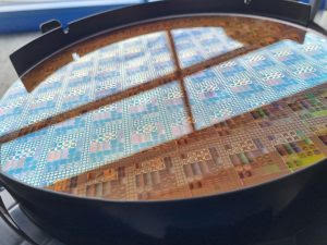
Addressing the 14th convocation of IIT Hyderabad, Union Minister Ashwini Vaishnaw declared a landmark achievement. India’s electronics exports have surpassed USD 40 billion an incredible eight-fold increase in just 11 years. The production of electronics within India grew six-fold during the same timeframe, a factor that lends credence to the manufacturing capability of the nation.
Important Highlights from Vaishnaw’s Address:
Exports & Production Growth: Electronics production has grown 6× and the exports 8× during the last 11 years, sustaining double-digit CAGR.
Semiconductor Ambitions: The commercial production of the first Made-in-India semiconductor chip is expected to be seeded by the end of this year. India aspires to become one of the top five semiconductor countries in the near future.
Telecom Stack Success: A fully indigenous 4G telecom stack was created in just 3½ years and is now powering ~90,000 towers, more than the networks in many countries.
5G Labs & Talent Building: The government has rolled out 100 5G labs, having distributed EDA tools from Cadence, Synopsys & Siemens to over 270 colleges and institutions (including startups, the number increases to 340) for the fostering of semiconductor design talent.
Infrastructure Boost: Vaishnaw also discussed the quick development of Mumbai-Ahmedabad, India’s first bullet train, which is expected to start operations in August or September 2027.
These achievements highlight the Modi government’s efforts to create a self-sufficient electronics ecosystem that includes chip design, telecommunications, and semiconductor manufacturing under the Make-in-India project.
The electronics export stood at an estimated USD 12.41 billion in Q1 FY26 (April-June), with year-to-year growth clocking an impressive 47%. The chief markets for Indian electronics export were the United States (60.2%), the UAE (8.1%), and China (3.9%), marking India’s ascension on the global map of electronics manufacturing.
The growth in Q1 confirms India’s status as a developing center for electronics production and makes a significant contribution to the USD 40 billion annual export milestone.
The Significance of This Leap:
- Global Market Integration: Dominance of markets like US, UAE, and China signals deeper integration of India into global supply chains.
- Security and Self-Reliance: Indigenous telecom stack and semiconductor push furthers the national security and reduces import dependency.
- Job Creation and Skill Building: Economic boom arising from semiconductors, EDA labs, and 5G infrastructure projects is creating demand for skilled professionals.
- Strategic Infrastructure Synergy: By collaborating with major projects like telecom, railroads, and bullet trains, the growth of electronics supports national modernization
Conclusion:
Rising electronics exports in India with the scaling-up of manufacturing processes crystals the evolution of a manufacturing ecosystem aligned with the Make-in-India initiative. The assurance of indigenous semiconductors, solid telecom backdrop, and a talent pipeline pave India’s way as an electronics and technological hub across the world.
The post India’s Global Rise in Electronics Backed by $40B Exports, Says Vaishnaw appeared first on ELE Times.
Nexperia and TU Hamburg launch endowed chair in power electronics
Renesas adds 650V GaN FETs for high-density power conversion
Сторінки

