
Збирач потоків
Digital isolators strengthen industrial systems

Part of Diodes’ RobustISO family, the API782x series of dual-channel digital isolators delivers 5.7-kVRMS isolation for 1 minute per UL 1577. The devices offer reliable protection for digital control and communication signals in solar inverters, motor control, industrial automation, and data center equipment.

The API782x series meets reinforced and basic isolation requirements across multiple standards, including VDE, UL, and CQC. The devices are rated for an 8-kV peak isolation voltage per DIN VDE 0884-17 and a 12.8-kV peak surge isolation voltage for transient events. Based on Diodes’ reliability calculations for the capacitive isolation barrier, the components offer a predicted operational lifetime exceeding 40 years.
The isolators support data rates up to 100 Mbps and provide a minimum CMTI of 150 kV/µs. The API7820 features both channels in the same direction, while the API7821 provides both channels in the opposite direction with either a high or low default output state. They operate from a 2.5-V to 5.5-V supply voltage and typically consume 2.1 mA per channel at 1 Mbps.
API782x isolators in SO-16WW packages are available through Diodes’ authorized distributors.
The post Digital isolators strengthen industrial systems appeared first on EDN.
DSC integrates control, sensing, security

Microchip’s dsPIC33AK256MP306 digital signal controller (DSC) combines a 200-MHz, 32-bit core and double-precision FPU with high-resolution PWMs and high-speed ADCs. It also includes a hardware crypto accelerator with support for post-quantum cryptography (PQC). Offered in a 36-pin VQFN package, the DSC saves space and simplifies PCB layout in power conversion, motor control, and intelligent sensing applications.

The dsPIC33AK256MP306’s four PWM generator pairs (eight outputs) deliver fine edge placement (FEP) resolution down to 78 ps. Three 12-bit SAR ADCs operate at up to 40 Msamples/s, alongside 5-ns comparators and 12-bit DACs with slope compensation. These features enable fast, deterministic control loops for high-efficiency DC/DC converters, auxiliary rails, and high-frequency SiC/GaN systems. An integrated touch controller extends support to sensing and HMI functions.
To address growing cybersecurity requirements, the dsPIC33AK256MP306 family supports secure boot, firmware updates, and debug, with hardware-accelerated PQC aligned to emerging standards for connected control systems. Live update capability maintains uninterrupted firmware upgrades in high-availability systems.
Prices for the dsPIC33AK256MP306 start at $1.97 in lots of 5000 units.
dsPIC33AK256MP306 product page
The post DSC integrates control, sensing, security appeared first on EDN.
Vexlum and Menlo collaborate to streamline optical clock development
Engineering tradeoffs: a camera case study

Four cameras, from two companies. Similar at first glance. Quite different once you zoom in and ponder the picture a while. Which approach is superior? Share your opinions in the comments!
The way this is going, and to remain honest both with myself and all of you, I’m at least for now going to need to start referring to myself as a “camera collector” versus a photographer. I keep accumulating particularly noteworthy (therefore also rare) gear when I come across lightly used, but still reasonably priced, examples on eBay and elsewhere. But I can’t seem to find any spare time to actually use anything in my steadily expanding hardware inventory…at least not yet.
Will I ever be able to retire?First World problem. I know. My latest examples of acquisition excess fall into the “pocketable” camera category. First off are two Pentax devices. As regular readers may recall from my past writeups, I’m nearing a half-century as a “Pentaxian”, a term originating on a t-shirt I snagged at the company’s CES booth a “few” years ago, prior to the brand’s acquisition by Ricoh. The new-to-me cameras are both members of the company’s “Q” product series: a first-generation Q:

and the successor Q7, skipping (at least so far) the in-between Q10 as well as the Q-S1 concluding iteration. I’d long known about the Q family, which originated a decade-and-a-half back, but enthusiastic reviews from folks such as Micro Four Nerds (the prior blog link is supplemented by the following video) tipped me over the acquisition edge:
Key differences between my two Pentax Q-series cameras include:
- Sensor size: 1/2.3″ on the Q, 1/1.7″ on the Q7, albeit both delivering 12 Mpixel resolution. By the way, the origin of this particular sensor dimension terminology is a story in and of itself, which I’ll save for another day; for now, see here.
- Body construction: Magnesium alloy on the Q, (still-rugged) plastic on the Q7
Note too, for comparison-to-come purposes, that neither model embeds an electronic viewfinder (EVF), although they both include both a pop-up flash and a hot shoe tailored for an optional external flash unit (which can operate in tandem with the pop-up) or a transmitter.
Potato, potahto (or tomato?)Then I came across Chris Niccolls’ extensive writeup, “The Panasonic Lumix GM-5 Is the Greatest Digital Camera Ever Made”, along with an associated video, at PetaPixel:
Insert hook and reel me in. Regular readers may also recall I’ve been slowly-but-steadily collecting Micro Four Thirds (M43) gear in recent years, now spanning a “few” cameras from two suppliers (Olympus-now-OM System and Panasonic; the Blackmagic Design video cameras I own are both higher-end Canon EF mount-based models), one of which ended up as a gift for my wife. Well, my stable is now even fuller; I bought both a Panasonic Lumix DMC-GM1:

and the successor DMC-GM5:

both of which are also more than a decade old at this point. Here’s another Micro Four Nerds review writeup-plus-video combo, this time focused (bad pun intended) on the GM1:
along with a coverage content tandem on the GM5 (to be clear, I have no affiliation with Micro Four Nerds or any other “influencer” showcased here; I’m just a fan):
Notable differences between the two models include the following:
- Supplemental illumination: pop-up built-in flash on the GM1 (but no hot shoe), hot shoe (but no integrated flash) on the GM5, and
- Viewfinder: backside LCD only on the GM1, added EVF (electronic viewfinder, space-supplanting the predecessor’s pop-up flash) on the GM5
Although the four cameras, from two manufacturers’ model lines, are conceptually similar (“pocketable”), their respective implementations are quite different. The inherent tradeoffs leading to each development team’s decisions and resultant product capabilities and limitations are interesting (IMHO at least) to ponder. Note that I have no company-representative insight, either quotable or off-the-record; what follows are just my educated guesses.
As already mentioned, my two Pentax Q variants’ image sensors are both 12 Mpixel in resolution, albeit with differing dimensions; the ~60% larger-area of the Q7’s sensor translates into improved low-light performance and wider dynamic range thanks to expanded pixel pitch and other factors. Conversely, the Panasonic GM1 and GM5’s image sensors are, as far as I can tell, identical, with 16 Mpixel resolutions. That said, M43 image sensors have roughly 9x the surface area of the 1/2.3″ sensor in the Pentax Q, and are still approximately 4x larger (again, surface area, not necessarily active image capture area) of the 1/1.7″ sensor in the Pentax Q7.

All four (total, including my two) Pentax Q family members also supported in-body image stabilization (IBIS), in and of itself a curious choice given the lightweight bodies and accompanying lenses, all of which would seemingly diminish the need for mechanical stabilization of any sort. To wit, neither Panasonic camera mentioned here implements IBIS, nor did any Panasonic-branded M43 lenses support optical image stabilization (OIS), at least at the time that the GM1 and GM5 were in production.
That said, M43 partner then-Olympus did have OIS-inclusive optics in its “glass” portfolio at the time, which could as-needed be used on Panasonic bodies given the two manufacturers’ lens mount compatibility. OIS is, generally speaking, inferior to IBIS, although as I’ve previously noted, it’s particularly effective with telephoto lenses. But it’s arguably better than nothing at all, or to interpolation-based digital image stabilization, for that matter.
Here are a couple of example videos discussing the similarities and differences between IBIS and OIS along with concept examples of both IS forms in action, as well as how they can collaborate:
This one from Canon has a Japanese audio track albeit with English subtitles:
Keep in mind, too, that given the Panasonic cameras’ larger-sized image sensors versus the Pentax alternatives, therefore larger pitch pixels despite the 33.3% higher resolutions, image stabilization was inherently less necessary in the M43 case given that improved light-gathering capability translated into the ability to operate them at blur-suppressing higher shutter speeds.
Space constraintsThe added stabilization hardware surrounding the image sensor in the Pentax Q-family bodies, coupled with the desire to maintain their compact weight and dimensions, also compelled the company to dispense with a mechanical shutter, at least in the bodies themselves. Instead, a subset of the then-available eight-lens suite embedded mechanical leaf shutters in the lenses. More broadly, an “electronic shutter” implemented in the image sensor was available in all body-plus-lens cases, albeit with “rolling shutter” and other tradeoffs.
A hollow victory?Ironically, in spite of these likely-difficult tradeoff decisions made by its development team, Pentax still ended up with Q-series camera bodies that were (slightly) larger than that of the Panasonic DC-GM1, as Robin Wong, another well-known photo enthusiast “personality”, notes in his Pentax- and Panasonic-themed blog posts and videos:
I’ve got more to say about the two companies’ contrasting approaches to the “pocketable” camera market, including the tradeoffs between multi-supplier standard and sole-sourced proprietary lens mounts …but I’ll save that for another day and writeup (or few). For now, I’ll wrap up my writeup and hand the keyboard to you for your so-far thoughts in the comments!
—Brian Dipert is the associate editor, as well as a contributing editor, at EDN Magazine.
Related Content
- The Godox V1 camera flash: Well-“rounded” with multiple-identity panache
- Scrutinizing a camera flash transmitter
- Multi-source vs proprietary: photography case studies
- SD card speeds: question your assumptions
- Tamron’s TAP-in Console: A nexus for camera lens update and control
The post Engineering tradeoffs: a camera case study appeared first on EDN.
Sasken Announces Hyderabad Center of Excellence to Scale Product Engineering and Digital Innovation
Hyderabad, India: April 16, 2026: Sasken Technologies Ltd. (BSE: 532663, NSE: SASKEN), a leading provider of product engineering and digital transformation services, today announced the launch of its Center of Excellence (CoE) in Hyderabad. The new center strengthens Sasken’s regional delivery footprint and deepens collaboration with strategic Chipset customers like Qualcomm and their OEMs.
Located in one of India’s fastest-growing technology ecosystems, the Hyderabad CoE will focus on next-generation engineering across connected devices, 5G-led platforms, IoT solutions, embedded systems, and digital product engineering. The center is designed to enable closer customer collaboration, accelerate engineering cycles, and support faster product innovation for complex global programs across industries such as Automotive, Smart devices, HiTech, Satellite communication, Industrial etc.
As part of this expansion, Sasken also announced the appointment of Nirmala Datla, Chief Data Science & Engineering Officer, as Site Leader for the Hyderabad CoE. She will drive delivery excellence, build next-generation engineering capabilities, and lead talent development from the location.
Alongside the leadership appointment, Sasken plans to hire initially 100+ specialized professionals from Hyderabad’s strong technology talent ecosystem in the coming months. Hiring will focus on high-skill roles across semiconductors, ODM, automotive, and Data Science & Engineering, supporting advanced engineering programs in connected devices, intelligent platforms, and next-generation digital ecosystems for global customers.
“The Hyderabad CoE represents a strategic investment to support the growing demand for Sasken’s capabilities in product engineering and digital transformation. Hyderabad’s strong engineering talent ecosystem enables us to scale delivery, deepen customer collaboration, and accelerate innovation and time-to-market for our customers,” said Nirmala Datla, Chief Data Science and Engineering Officer, Sasken Technologies.
“Hyderabad presents us with an excellent talent pool across our BU’s. The launch of this Center of Excellence strengthens Sasken’s delivery footprint and positions us to support customers with greater speed, scale, and proximity,”. “Aligned with our growth strategy, we continue to make focused investments in talent and capabilities that enable us to scale the right segments and deliver sustained growth.” said Hareesh Ramanna, Chief Experience Officer, Sasken Technologies.
The post Sasken Announces Hyderabad Center of Excellence to Scale Product Engineering and Digital Innovation appeared first on ELE Times.
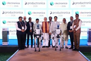
India sharpens its electronics manufacturing edge at electronica India and productronica India 2026 in Greater Noida
- Visitor turnout: 20,922 participants, including key buyers and sourcing decision-makers, turn up for the Greater Noida edition.
- Business engagement: The event facilitated 1,500+ buyer-seller meetings, focused on localisation, supplier discovery, and supply chain partnerships
- International presence: Strong participation from countries like Germany, China, Japan, Taiwan, and the United States
Greater Noida: India’s ambition to position itself as a global electronics manufacturing hub is beginning to reflect in more concrete ways; on factory floors, in policy corridors, and increasingly, on industry platforms where supply chains are being actively reshaped.
The 2026 Greater Noida edition of electronica India and productronica India brought this shift into focus, with a strong turnout of global suppliers, domestic manufacturers, and sourcing leaders. For an industry navigating geopolitical realignments and cost pressures, the event served less as a showcase and more as a working marketplace. The event was attended by 20,922 participants and brought more than 1000+ suppliers and distributors from across the globe and India to the show floor.
The Government of Uttar Pradesh, as the Host State, played a key role in supporting electronica India and Productronica India 2026 in Greater Noida. Its partnership reflected the state’s continued focus on building a strong electronics manufacturing ecosystem, backed by policy support, infrastructure development, and investment facilitation. The presence and involvement of senior government representatives underscored Uttar Pradesh’s intent to position itself as a preferred destination for electronics manufacturing, while also enabling closer engagement between industry stakeholders and policymakers on the ground.
Therefore, the inauguration was led by a cross-section of political and industry leaders, including Shri Suresh Kumar Khanna, Uttar Pradesh’s Minister for Finance and Parliamentary Affairs, and Shri Jitin Prasada, Union Minister of State for Electronics and IT, and for Commerce and Industry. They were joined by Shri Nand Gopal Gupta ‘Nandi’, Minister for Industrial Development; Shri Sunil Kumar Sharma, Minister for IT & Electronics; Shri Ajit Singh Pal, Minister of State for Science and Technology, Electronics and IT; and Shri Alok Kumar, Principal Secretary, IT & Electronics, Uttar Pradesh.
Scale with direction
Across its dual editions in Greater Noida and Bengaluru, the platform now brings together over 60,000 participants annually, reflecting a 50% expansion in scale and reinforcing its position as a key industry meeting point.
The Greater Noida edition saw significant participation from key manufacturing economies, including Germany, China, Japan, Taiwan, and the United States—an indicator of India’s increasing integration into global value chains.
More notably, 1500+ structured and on-ground B2B meetings were conducted during the event, many centred on supplier diversification, localisation strategies, and lead-time optimisation. These are areas that have moved to the top of boardroom agendas as companies reassess dependence on concentrated supply bases.
The current edition reflected a clear emphasis on capability building. Exhibitors pointed to growing interest in component manufacturing, automation, and supply chain resilience. Buyers, particularly from sectors such as automotive and consumer electronics, were seen evaluating domestic suppliers with an eye on long-term partnerships rather than short-term procurement.
Alongside the exhibition, a series of conferences provided a forum for more detailed engagement, aligning with the sector’s current priorities, addressing policy, supply chain resilience, automotive electronics, PCB manufacturing, and advanced production technologies. These themes were explored through platforms such as the UP Electronics Leadership Summit, the ELCINA Supply Chain Summit, the Automotive Display Conference by ICEA, the Bharat PCB Tech Conference, and the SMT Thought Leadership Summit.
The edition also emphasised innovation, featuring a Startup Pavilion supported by the Government of Uttar Pradesh and curated industry podcasts. A notable development was the launch of BPCA, Bharat’s dedicated platform for printed circuits and assemblies, introduced in collaboration with ELCINA and Messe Muenchen India.
Industry bodies such as ELCINA and ICEA were active participants, contributing to both conference discussions and closed-door industry interactions.
Rajoo Goel, Secretary General, ELCINA, stated,“The conversations at electronica India and productronica India 2026 reflected a clear shift in industry priorities. Localisation has moved beyond policy intent and is increasingly becoming a business imperative. The platform brought the value chain together in a way that enabled more practical discussions around strengthening component manufacturing capabilities and reducing external dependencies.”
Pankaj Mohindroo, Chairman, ICEA, added, “What stood out clearly was the growing maturity of India’s electronics ecosystem. We are now seeing a far stronger convergence between policy direction, industry investments, and supply chain strategies, an alignment that is critical for sustainable scale.
electronica and productronica India 2026 played an important role in advancing this momentum by enabling meaningful, direct engagement between global technology and component suppliers and Indian manufacturers who are expanding with long-term commitment and strategic intent.”
Voices from the floor
Participants indicated that the value of the platform lay in the quality of engagement rather than scale alone.
Tsuyuki Junichi – Division Head – Robotics Support Business Division, Yamaha Motor India Sales (P) Ltd said, “For Yamaha Motor India Sales (P) Ltd., electronica India and productronica India, opened more meaningful conversations with teams that are actively planning their next phase of manufacturing growth.”
Mr. Narendra Savant – VP Operations, Kyoritsu Electric India Pvt Ltd stated, “What stood out for us at electronica India and productronica India 2026 in Greater Noida was the clarity of intent from buyers. They came with defined sourcing requirements, timelines, and technical expectations. We saw strong interest across diverse industrial manufacturers for our Customised Robotic + Automation Integrated solutions and our Made-in-India End-of-Line Testers, which aligns with where the Indian electronics manufacturing production needs are heading. For us, the value of this platform lies in the ability to engage with decision-makers who are actively evaluating long-term supply partnerships rather than short-term procurement.”
Raj Kumar Saini – Managing Director, Saini Communications Pvt Ltd, mentioned,“The quality of interaction has definitely gone up. We’re no longer talking about basic automation; most conversations are now around integration, efficiency, and how to scale operations. We’ve had interest coming in from multiple sectors, which is a good sign. You can see that manufacturers are thinking more long-term now, and that changes the kind of discussions you have.”
Visitors highlighted the ability to evaluate global and domestic suppliers within a single platform, enabling faster decision-making.
Robins N T – Head Strategic Sourcing & New Product Development, Simple Energy said, “We are actively looking at diversifying supply chains and increasing localisation, and the interactions here help accelerate that process. The level of preparedness among exhibitors has improved significantly, which makes it easier to move from evaluation to actual business discussions within a short span”.
Srinivasan Sampath – Head NPD Materials at Pricol Limited, said, “What worked well for us at electronica India and productronica India 2026 in Greater Noida was the ability to benchmark multiple suppliers side by side. It helped us compare capabilities, timelines, and approach in a very practical way. In a short span, we were able to narrow down options that would have otherwise taken months to evaluate.”
Anuj Kumar Srivastava – Global Head- Facilities, Secure Meters Ltd. mentioned, “We came in to understand how quickly suppliers in India are adapting to new requirements, especially around quality standards and turnaround times. The interactions here gave us a clearer picture of who is ready to scale and who we can work with as we expand and diversify our operations. Pleased to see focus on Make in India.”
The event also witnessed strategic announcements and MoUs, including expanded collaborations between international PCB and component associations and Indian industry bodies, aimed at strengthening supply chain capabilities and fostering technology exchange.
Dr Reinhard Pfeiffer, CEO, Messe München, said, “What is becoming evident is how quickly India is moving from being part of the conversation about the supply chain to influencing it. Companies no longer assess the country solely based on cost or scale; they are also looking at long-term manufacturing alignment. This shift is reflected in the discussions taking place at electronica India and productronica India 2026 in Greater Noida.”
Bhupinder Singh, President – IMEA, Messe München & CEO, Messe Muenchen India said, “electronica India and productronica India are increasingly reflecting what the industry is dealing with in real time, supply chain adjustments, localisation, and the need for reliable partners. The conversations here are more structured, more practical, and closely linked to actual business decisions, which is where their relevance comes from.”
Looking ahead
The second edition of electronica India and productronica India 2026 is scheduled to be held in Bengaluru from September 16 to 18, 2026, extending the platform’s reach into another major electronics manufacturing hub.
As the industry recalibrates in response to geopolitical and economic shifts, platforms such as these are likely to play a more central role. The question, increasingly, is not whether India will be part of the global electronics supply chain—but how large a role it intends to occupy.
The post India sharpens its electronics manufacturing edge at electronica India and productronica India 2026 in Greater Noida appeared first on ELE Times.
Aixtron’s preliminary Q1 order intake up 30% year-on-year, driven by Opto comprising 65% share
JLCPCB is not worth it for me, now
 | I used to use PCBWAY years back for a long time, doing over 100 high value jobs with them and they were good. I never had any real complaints. I moved over to JLCPCB due to the majorly lower cost a few years ago and to be honest I also couldn't complain with their service for a good amount of time. I have been using them for prototyping for about 3 years with the occasional small batch run up to 200 pieces of fairly basic stuff like ESP32 etc. Recently I have started a small business that uses a reasonbly complex setup of USB at 5Gb/s and MIPI CSI at 2Gb/s with the corresponding high value parts of the image sensor and CYUSB CX3 transceiver. I have now made 4 batches. Batch 1 of 5 pieces: Batch 2 of 5 pieces: Batch 3 of 25 pieces: Batch 4 of 5 pieces: Every time I order a batch I get a different outcome. No question JLCPCB uses fake parts intentionally or unintentionally. The outcome is the same. For me I'm going to be moving to a alternative Chinese supplier with free issued parts. [link] [comments] |
Quinas completes Innovate UK project advancing ULTRARAM for AI and neuromorphic computing
💛💙 Запрошуємо ветеранів на ознайомчий курс «Передові технології прикладної механіки та біомедичної інженерії».

Ветерани та ветеранки, хочете здобути нову професію у сфері, де інженерія й медичні технології працюють на реальні потреби людей?
Here is a possibly novel joule thief
 | There's not a lot of love for the JT these days. Nevertheless they crossed my mind the other day and I couldn't help but put one together. I was as always amused by their ability to drive an led from incredibly low voltage. I had it down to 0.39V at one point. The age old issues cropped up immediately when I wanted to make an led last on a button cell for a long time. They're great at pulling out some juice at low voltages, but not so good when the cell is brand new. Which is a shame. If one of these could take advantage of all the power in a button cell, they'd last much much longer obv. There's all kinds of regulated varieties on the internet. Most of them rely on negative feedback at the cost of high base (or drive) current. In many cases, the amount of power being consumed by the base circuit was using more power than the led itself. This is primarily due to using a low value resistor into the base of a bjt. To regulate the power (often voltage), a second transistor diverts some of the current to ground. As power consumption grows, more base current is diverted until these balance out over the range of input voltages. If the drive current and positive feedback could be controlled without wasting most of it, a ton of power could be saved. So I came up with this; a jfet between L2 and the base resistor. Instead of diverting current in the bias circuit to ground, it is directly regulated with a variable "resistance." Of course to control the jfet would require a floating negative voltage that was proportional to the power being consumed by the boost circuit. So I added an additional winding, L3, to provide an isolated supply that would rise and fall with the rest of the joule thief. Then it was a simple matter of using a low power (low Vf diodes and small ceramic caps) rectifier with a pot to dial in the control voltage. Jfets have an incredibly high impedance, and I used a 2 megaohm pot so the control circuit utilizes very little power. Anyway I've been rambling. I thought the idea was neat and now I have a working version to see how long it lasts. If anyone is interested, I can post a schematic. This is nothing special, but a fun detour from the actual projects I've been working on. [link] [comments] |
I finally finished hand soldering this stupid 7 segment display
 | My spine hurts all over. 201 leds are smaller than a grain of salt! Even harder to solder on a home made pcb! Plus all the time troubleshooting broken tracks and drilling holes by hand. Those blobs kf solder you see are vias that link the rear and front copper tracks together. Did I mention my spine hurts? [link] [comments] |
WD40 Contact Cleaner
 | “The use of WD-40 Specialist Contact Cleaner may result in damage to the laptop motherboard and is therefore not recommended for such applications.” [link] [comments] |
Workbench bonanza
 | This i my workbench in the basement. Really happy with the layout and space. MIssing basically nothing more than a real heating system. At the moment working on a testjig for a pcb [link] [comments] |
US DOE selects five project to restart domestic primary gallium recovery
Rate my bench (When it’s clean)
") | This bench of mine has served me well for many projects including fixing a lot of things for family and friends. My current project is fixing that vacuum tube oscilloscope in the 5th picture. I’m also currently rearranging my drawer layout so things are still half labeled at the moment. [link] [comments] |
The system architect’s sketchbook: The AI hiring frenzy


Deepak Shankar, founder of Mirabilis Design and developer of VisualSim Architect platform for chip and system designs, has created this cartoon for electronics design engineers.
The post The system architect’s sketchbook: The AI hiring frenzy appeared first on EDN.
Nuvoton Releases an Industry-Leading-Class High-Power Violet Laser Diode (402 nm, 4.5 W) 1.5 times higher output than our conventional product
Kyoto, Japan, April 15, 2026 – Nuvoton Technology announced today the start of mass production of a “high-power violet laser diode (402 nm, 4.5 W) ” that achieves industry-leading class optical output in a 9.0 mm diameter CAN package (TO-9). This product achieves 1.5 times the optical output compared to our conventional product through our proprietary device structure and heat dissipation design technology, and contributes to improving production throughput in optical equipment such as maskless lithography systems. Furthermore, adding this product to our lineup enables our product portfolio to support major photosensitive materials used in advanced semiconductor packaging.
Achievements:
- Achieves 4.5 W high-power at 402 nm, 1.5 times that of our conventional product, enhancing production throughput in maskless lithography systems
- Expands our lineup of light sources for maskless lithography in advanced semiconductor packaging, supporting multiple major photosensitive materials
- Expands the lineup of mercury lamp replacement solutions [6] , providing new options in light source selection
For more product details, please see here: https://nuvoton.co.jp/semi-spt/apl/rd/?id=1100-0272
Features of New Product:
- Achieves 4.5 W high-power at 402 nm, 1.5 times that of our conventional product, enhancing production throughput in maskless lithography systems
Violet (402 nm) laser diodes generally suffer from relatively low wall-plug efficiency [7] and significant self-heating, and are also prone to short-wavelength-induced degradation, which makes stable high-power operation difficult.
To address these challenges, the “device structure that enhances wall-plug efficiency (WPE)” and the “high thermal conduction package technology that effectively dissipates heat,” which were used in the high-power ultraviolet laser diode [8] (379 nm, 1.0 W) announced as a new product in January 2026, have been expanded to the violet (402 nm) band.
As a result, we are launching a “high-power violet laser diode (402 nm, 4.5 W)” that achieves 1.5 times the optical output compared to our conventional product. In particular, by applying our proprietary facet coating technology that suppresses degradation factors at the laser facets, we have improved the lifetime performance during high-power operation, and by adopting a monolithic molded structure using high heat dissipation materials for the package, we have improved heat dissipation performance.
By achieving both “high-power” and “high reliability”, this product enhances production throughput in industrial optical equipment where high quality is required.
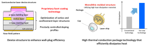
| Figure 1: “Device structure that enhances wall-plug efficiency” and “High thermal conduction package technology that effectively dissipates heat” |
- Expands our lineup of light sources for maskless lithography in advanced semiconductor packaging, supporting multiple major photosensitive materials
This product will deliver significant value in maskless lithography for advanced semiconductor packaging, a market that is rapidly growing, driven by expanding demand for artificial intelligence (AI) and other applications.
In circuit formation for advanced semiconductor packages, maskless lithography technology that directly exposes (draws) wiring patterns based on design data has been attracting attention in recent years, as it enables not only cost reduction and development period shortening, but also high-precision patterning correction in response to substrate warpage and distortion.
For laser diodes, which are one of the main light sources in this maskless lithography technology, there has been a demand for compatibility with wavelengths close to the i-line (365 nm) and h-line (405 nm), which are the emission lines of mercury lamps, in order to correspond to the main photosensitive materials, as well as higher output for the purpose of improving the production throughput of equipment.
In addition to the “high-power ultraviolet laser diode (379 nm, 1.0 W)” for i-line applications announced in January 2026, we are adding this new product, “high-power violet laser diode (402 nm, 4.5 W) “, for h-line applications to our lineup.
This expansion strengthens our lineup of light sources for maskless lithography in advanced semiconductor packaging, enabling consistent support for multiple major photosensitive materials while contributing to higher production throughput of equipment.
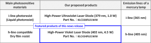
| Table 1: Major Photosensitive Materials in Maskless Lithography for Advanced Semiconductor Packages and Our Proposed Products |
- Expands the lineup of mercury lamp replacement solutions, providing new options in light source selection
This product will be newly added to the lineup of our “semiconductor laser-based alternatives to mercury lamps.” The h-line (405 nm), which is an emission line of mercury lamps, is used in a wide range of fields such as photocuring, 3D printing, sensing, biomedical applications, and marking, and this product provides customers with a new option as an alternative light source for these applications.
Furthermore, by leveraging the high-power performance that is a feature of this product, it will contribute to improving the efficiency of processes that were difficult to realize in the past, as well as to the creation of new optical applications.
| Figure 2: “Mercury Lamp Replacement Solution Using Semiconductor Lasers” Developed by Our Company |
This product is scheduled to be exhibited at our booth at “OPIE’26” to be held in Yokohama, Japan.
Applications:
- Maskless lithography
・ Resin curing
・ Sensing
・ Marking
・ 3D printing
・ Biomedical
・ Alternative light source for mercury lamps, etc.
Product name:
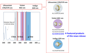
KLC434FL01WW
Specifications:
| Part number | KLC434FL01WW |
| Wavelength | 402 nm |
| Optical Output Power | 4.5 W |
| Package Type | TO-9 CAN |
Start of mass production: May 2026
The post Nuvoton Releases an Industry-Leading-Class High-Power Violet Laser Diode (402 nm, 4.5 W) 1.5 times higher output than our conventional product appeared first on ELE Times.
Mission accomplished: Infineon technology proves reliable once again in space on Artemis II
- Infineon’s radiation-hardened semiconductors performed flawlessly on NASA’s Artemis II Orion capsule across ten days in space.
- Since the 1970s Infineon’s radiation-hardened technology has proven reliable across hundreds of space missions.
- With the world’s first JANS-qualified internally manufactured rad-hard gallium nitride (GaN) transistor, Infineon sets the benchmark for space semiconductors.
Munich, Germany – 15 April 2026 – NASA’s Artemis II mission has successfully returned to Earth after ten days in space, having approached the Moon and reached the farthest distance from our planet ever achieved by crewed spaceflight. The four astronauts have safely returned home, delivering renewed proof that the radiation-hardened (rad-hard) semiconductor solutions of Infineon Technologies AG (FSE: IFX / OTCQX: IFNNY) perform reliably even under the most extreme conditions of deep space. From critical power supply and control systems to data communications, Infineon’s rad-hard devices from its IR HiRel (high reliability) division supported the electronic backbone at the heart of the Orion capsule.
“Space programs require technologies and partners they can rely on for decades. Infineon is a critical technology partner, and we are proud to have once again contributed to the success of a historic space mission,” said Mike Mills, Senior Vice President and General Manager of IR HiRel at Infineon. “The space industry is evolving rapidly: more missions, more data, more electrification – while facing increasing pressure on size, weight and power consumption. In this equation, semiconductors are becoming a central focus in space. The fact that our components performed flawlessly from the first to the last minute of the Artemis II mission is no coincidence. It is the result of decades of engineering expertise, state-of-the-art qualification processes and a deep understanding of what semiconductors must deliver in space.”
Artemis II marks decades of space heritage for Infineon. As far back as the 1970s, Infineon’s predecessor companies supplied the first rad-hard components for NASA and ESA space programs. Since then, Infineon IR HiRel has supported hundreds of space missions including navigation satellites, the International Space Station (ISS), and today’s Artemis program. Our rad-hard components have traveled further than any other human-made object, over 20 billion kilometers from Earth. As a technology leader, Infineon continues to invest in, develop and manufacture the best performing rad-hard semiconductors supporting the space design community on a global scale.
The demands placed on semiconductors in space are immense. Beyond Earth’s protective magnetic field, high-energy particles strike electronic components unimpeded and can permanently damage or destroy them, causing mission failure. Infineon’s rad-hard technology addresses these mechanisms not through passive shielding, but through a semiconductor architecture that is radiation-resistant by design. All products are qualified to the most stringent international space standards, including MIL-PRF-38535 Class V, MIL-PRF-19500, ESA’s ESCC standards and NASA EEE-INST-002, ensuring their reliable performance.
At Infineon, innovation is developed at the system level: semiconductor technology, rad-hard assurance, and packaging perform together. An optimized overall system influences not only electrical performance, but also thermal behavior and long-term reliability – while simultaneously reducing weight and volume. Every gram counts in space, Infineon’s rad-hard parts provide a decisive system-level advantage.
Wide-Bandgap technology: GaN takes the next step
Infineon is also advancing the use of new semiconductor materials in space applications. Gallium nitride (GaN) enables lower switching losses, higher power density and higher switching frequencies – reducing power losses and magnetic component requirements, which translates directly into further weight savings. Built on internal manufacturing capabilities and the process and quality stability that comes with it, Infineon’s award-winning rad-hard 100-V GaN transistor, qualified to JANS (Joint Army Navy Space) per MIL-PRF-19500, brings GaN from concept to proven technology for demanding space missions. Infineon’s JANS qualified device is the first and only internally manufactured rad-hard GaN transistor on the market.
Infineon offers a broad rad-hard portfolio spanning Si power MOSFETs and GaN transistors, gate drivers and solid-state relays, in addition to rad-hard memories and radio frequency (RF) devices. Backed by in-house radiation testing capabilities and guaranteed long-term product availability, Infineon positions itself not merely as a component supplier, but as a strategic technology partner for the entire space industry.
The post Mission accomplished: Infineon technology proves reliable once again in space on Artemis II appeared first on ELE Times.
Give bare-metal multicore processing a try

Multicore processing boosts performance and energy efficiency in many coding situations. Bare-metal algorithms further enhance these benefits.
Many embedded firmware engineers have seemingly not yet tried multicore processing. Using processors with more than one core can actually make your architecture and coding easier. And the part you may find surprising is that setting up and using multicores processors is very easy to do.
Wow the engineering world with your unique design: Design Ideas Submission Guide
Typically, multicore programs are used in systems with an OS, but if you’re like me, my projects are typically bare-metal. I have long used multicore under an RTOS but have historically avoided multicore on bare-metal systems. But ever since I discovered how easy it was to use multicore on bare-metal, it has become part of my go-to design architecture.
Let’s look at how this is accomplished. The examples and discussions that follow are based on using an RP2040 two-core microcontroller with code developed on an Arduino IDE. RP2040 development boards can be found for around $5 USD. Also, although I will discuss a two-core setup, expanding to larger core count processors will use the same concepts.
So why didn’t I use multicore designs sooner? I had some concerns that there were difficulties that I wasn’t ready to take on. Some of these were:
- How to keep each core’s code separate
- How to start multiple cores
- How the cores talk to each other (i.e., how to transfer data among cores)
- What peripherals each core can use; do they need to be checked out or registered, for example
It turns out that all these issues are actually very easy to deal with. Let’s look at them one at a time.
First, how do you separate the code for each core? In a single-core Arduino C program there are two major sections: the setup section (which begins like this: void setup()) and the loop section (which begins like this: void loop()). If you are using two cores, the first core, core 0, will use these sections just as used in a single-core design.
The code for the second core, core 1, will have a function defining its main loop. Let’s name it core1_main. Then in the core 0’s setup section, enter the line multicore_launch_core1(core1_main);. That line will start the function, called core1_main, running on the second core. (Note: I find it much cleaner to put the core 1 code in a separate tab in the Arduino IDE.) Unlike the main loop in an Arduino C program, you will need to wrap the code in core 1 in a while(1); loop. Another item to include is the line #include "pico/multicore.h" at the top of the code.
Be aware that there are other approaches for setting up code in the second core. They include methods that allow core 1 to use its own setup function. Use your favorite AI or other research tool to discover other methods of setting up code and executing code on the second core.
Here’s a very simple example having each core blinking its own LED:
#include #include "pico/multicore.h" // ----------------------------- // Core 1 code // ----------------------------- void core1_main() { pinMode(14, OUTPUT); while (1) { digitalWrite(14, HIGH); delay(500); digitalWrite(14, LOW); delay(500); } } // ----------------------------- // Core 0 code // ----------------------------- void setup() { pinMode(15, OUTPUT); // Start core 1 multicore_launch_core1(core1_main); } void loop() { digitalWrite(15, HIGH); delay(300); digitalWrite(15, LOW); delay(300); }This example gives you an idea of how to get the two cores executing their own tasks. Typically, though, you would want to have some sort of communication between the cores. This can be achieved very simply by using a variable that each core can see and modify. It turns out that the entire memory space of the microcontroller can be seen and modified by either core. So, if you define a global variable at the top of the code (just below the #include statements), it can be used to transfer data between cores.
Make sure that the variable is tagged as volatile as it can change at any time. Also remember that the RP2040 is a 32-bit microcontroller and reading and writing 64-bit values is not atomic, so care must be taken to not read a transferred 64-bit value before both halves have been transferred. A simple flag can help here. This simple method of using shared memory to transfer data is easy but can be dangerous if you’re not careful—similar to global variables—but bare-metal developers typically like this tight control over resources.
This method of transferring data is good for simple tasks, but you may want to use FIFOs to handle more data and to remove some syncing issues. These are not difficult to write, and you’ll also find pre-written packages online. For more sophisticated programs, you can investigate mailboxes, semaphores, flags, etc. from various sources…but now we’re getting into RTOS functions.
Now let’s look at sharing peripherals between cores. In our bare-metal architecture, the best explanation is that any core can use any peripheral at any time. This situation is both good and bad. Good because there are no flags to set, no checkouts that need to happen, and no negotiations to be made: just use the peripheral. Bad in the sense that without some form of coordination the two cores can attempt to set up the same peripheral at the same time, in different configurations.
What I have found useful in my designs is that I have typically separated the code in the two cores such that each core always uses peripherals that are not used by the other core. If that not the case in your designs, you may want to implement a resource lock method using flags. Related is the interesting fact that both cores can use the serial port (only configured by one core) without any necessary handshaking or flags. Do note, though, that the serial communications will be interleaved. That said, I find this very handy since I can Serial.print() from either core during debugging.
Let’s answer one last question: why do I want to use more than one core? The first reason is the obvious one: you get more computing power. But more than that, by separating tasks from each other you may find coding easier and cleaner. That’s because there are no concerns about the multiple tasks fighting for cycles, especially for time-sensitive tasks. Also, if you are using multiple interrupts, separating these tasks between cores can remove the complexity of interrupts occurring at the same time and thereby holding off one or the other. Another benefit is that you may have faster response to events happening as you can essentially monitor and respond to twice as many events.
Here’s another code example using some of the concepts discussed earlier. This code uses core 1 to monitor the serial port looking for a G or an R. If it sees a G, it sets the shared variable led_color to 1. Core 0 continuously monitors led_color and turns on the green LED if the led_color is 1. Similarly, if core 1 sees a R it changes led_color to 0 and core 0 then then turns on the red LED:
#include #include "pico/multicore.h" // ---------------------------- // LED pin assignments // ---------------------------- #define RED_LED_PIN 14 #define GREEN_LED_PIN 15 // ---------------------------- // Shared variable between cores // 0 = RED, 1 = GREEN // ---------------------------- volatile int led_color = 0; // ====================================================== // Core 1: Serial monitor // ====================================================== void core1_entry() { while (!Serial) { delay(10); } while (1) { if (Serial.available() > 0) { char c = Serial.read(); if (c == 'G' || c == 'g') { led_color = 1; Serial.println("Set LED = GREEN"); } else if (c == 'R' || c == 'r') { led_color = 0; Serial.println("Set LED = RED"); } } delay(2); } } // ====================================================== // Core 0 setup // ====================================================== void setup() { Serial.begin(115200); pinMode(RED_LED_PIN, OUTPUT); pinMode(GREEN_LED_PIN, OUTPUT); // Launch Core 1 multicore_launch_core1(core1_entry); } // ====================================================== // Core 0 loop — LED logic now lives here // ====================================================== void loop() { if (led_color == 1) { digitalWrite(GREEN_LED_PIN, HIGH); digitalWrite(RED_LED_PIN, LOW); } else { digitalWrite(RED_LED_PIN, HIGH); digitalWrite(GREEN_LED_PIN, LOW); } delay(5); }It may now be becoming clearer to you where the benefits lie in using more than one core. Think of something more complex, say, a program that monitors the serial port for modifications to settings, along with a high-speed ADC being read with a tight tolerance on jitter. Having the serial port code running on one core and the ADC code in another core would make this combination much easier to get working cleanly.
Give multicore code design a try! It’s easy, I think you’ll find lots of uses for it, and you’ll also find it makes coding easier and more organized.
p.s. Both pieces of code shown in this article were initially written by CoPilot per author instructions. The author subsequently only made minor modifications.
Damian Bonicatto is a consulting engineer with decades of experience in embedded hardware, firmware, and system design. He holds over 30 patents.
Phoenix Bonicatto is a freelance writer.
Related Content
- The next RISC-V processor frontier: AI
- Partitioning to optimize AI inference for multi-core platforms
- Multicore architectures, Part 1 – Key drivers
- Multicore architectures, Part 2 – Multicore characteristics
- Multicore architectures, Part 3 – Communications and memory
- Multicore architectures, Part 4 – Application specificity
The post Give bare-metal multicore processing a try appeared first on EDN.
Сторінки


![[link]](https://i.redd.it/l2ufxsag6jvg1.png)
![[link]](https://i.redd.it/ax218b5v4hvg1.jpeg)