
Збирач потоків
Modifying the INA226 Current Sensor for High-Power Applications
 | I’d like to share my experience building a "rough gauge" for my LiFePO4 battery pack. Instead of using an off-the-shelf Smart BMS, I chose the DIY route to better understand the underlying physics and processes. Stock INA226 modules come with a 100 mΩ shunt resistor, which limits the current measurement to a measly 800 mA. This is far too low for a power battery.
To find the exact resistance value, I ran a series of tests and compared the readings with a UNI-T UT61 multi meter. The calculated precision value is 4.392 mΩ.
The biggest challenge is heat. At currents above 10 A, the shunt begins to warm up noticeably. This creates Therm-EMF (the Seebeck effect), which causes "phantom" readings of about 50 mA on the screen for several minutes after the load is disconnected, until the node cools down. More details here: https://en.neonhero.dev/2026/02/modifying-ina226-from-08a-to-high-power.html [link] [comments] |
Test if the diodes work (Silly power supply for a lone lamp update)
") | A long anticipated update for "Silly power supply for a lone lamp" post :) The original post showed a simple set of low power batteries connected in parallel supplying a 12V/50mA lamp. The schematic featured a diode per battery to prevent them from feeding each other. Here, I decided to check experimentally if the diodes indeed work as expected. I used an STM32F103 module as multichannel ADC, a set of resistors to scale down from 0-18V to 0-3V and a RPi Zero 2W as a 5V power supply and to collect data. Potentiometers were set to 20k creating 6 100k/20k voltage dividers (pic 3). First, measured lamp and batteries voltages with a fresh set batteries. They held around 3 hours 45 minutes. The set had voltage around 12.6V fresh without load. Upon switching on the load they immediately dropped to 12V and then spent most of the time going from 10.5 to 8.5V as the pic 4 shows. The diodes took about 350mV so lamp's voltage went clearly below batteries. Then I mixed 3 fresh and 3 used batteries and actually was really surprised with how clearly it showed when used batteries kicked in. The last pic shows voltage drop across diodes and comparing with the previous one you can see that the diodes for used batteries open as voltage reaches around 200mV. Which is a great real-world demo of how low is cut-in (or knee) voltage for a Schottky diode can be (here SD103A used). [link] [comments] |
I hear we like to sort stuff here? How about a gallon of resistance?
 | submitted by /u/mofomeat [link] [comments] |
Weekly discussion, complaint, and rant thread
Open to anything, including discussions, complaints, and rants.
Sub rules do not apply, so don't bother reporting incivility, off-topic, or spam.
Reddit-wide rules do apply.
To see the newest posts, sort the comments by "new" (instead of "best" or "top").
[link] [comments]
NUBURU activates Q1 production ramp for 40 high-power blue laser systems
Звіт першого проректора КПІ Михайла Безуглого на засіданні Вченої ради 12 січня 2026 року

Функціонування університету в умовах визначеної невизначеності: причини для адаптації чи виклик новим можливостям
Safe operating area

Any semiconductor has limits on how much voltage, how much current, and for how much time combinations of voltage and current can be supported in normal usage. Sometimes that information is provided as part of the device’s datasheet, and sometimes that information is NOT provided. In either case, though, there ARE limits which MUST be observed.
Any switching semiconductor device must address voltage and current issues. Drive considerations aside, from the standpoint of “safe operating area” or SOA, the voltage Vds and the current Ids of a power MOSFET and the Vce and Ic of a bipolar transistor are at issue.
Please consider the following unwisely designed circuit in Figure 1.
 Figure 1 A badly designed switching circuit requiring the 2N2222 at Q1 to repeatedly dump the charge of capacitor C1 of 0.01 µF. Source: John Dunn
What we’ve done wrong here is require the 2N2222 at Q1 to repeatedly dump the charge of capacitor C1 of 0.01 µF. The Vce and the Ic versus time burdens on Q1 are as shown. The current peak of nearly 500 mA is pretty big, and to our dismay, it occurs while the value of Vce is still fairly high, which means that there is a substantial peak power dissipation demand placed on Q1.
Having constructed a Lissajous pattern of Vce versus Ic as shown in Figure 2, we process that pattern.

Figure 2 The voltage versus current Lissajous pattern for Q1. Source: John Dunn
Just one comment about obtaining that Lissajous pattern. The oscilloscope simulations in the Multisim-SPICE I was using do not support “x” versus “y” capability, and therefore cannot provide the Lissajous pattern. I made the pattern you see here by reading out the voltage and current values at each time step of the oscilloscope display and then plotting them using GWBASIC. There were 240 datums for each, a total of 480 readings, which were pretty tedious to acquire. Ordinarily, I can’t concentrate on work and listen to music at the same time, but this time, listening to some Petula Clark recordings through all of this did help to ease the monotony.
In all my years of acquaintance with the 2N2222, I have never seen any specification or any datasheet that presented the SOA boundaries for that device. In fact, I’ve never seen the SOA boundaries for any TO-18 packaged device. In the TO-5 and TO-39 packages, the one and only time I have ever come across SOA boundary information was for the 2N3053 and 2N3053A, and even today, some datasheets omit that information.
As a result, we just have to make do with what we’ve got, which for now is this partial reconstruction of the 2N3053 and 2N3053A SOA chart taken from a very old datasheet from RCA that I stashed away long ago (Figure 3).

Figure 3 Safe operating area reconstruction of the 2N3053 and 2N3053A SOA chart taken from a very old datasheet from RCA. Source: John Dunn
We replot the Vce versus Ic data using logarithmic scaling, and then we overlay that result with the SOA boundaries of our NPN, but we encounter a difficulty (Figure 4).

Figure 4 SOA examination using logarithmic scaling. Source: John Dunn
The 2N2222 has a peak power rating of 1.2 watts, while the 2N2219, a first cousin to the 2N2222, has a peak power rating of 3 watts, versus a 7 watts rating for the 2N3053. I would therefore imagine that the 2N2222 SOA boundaries are quite a bit lower than those of the 2N3053. We note that the SOA curve of Q1 operating in this circuit moves outside of the DC operating boundary for the 2N3053 and thus, in all likelihood, it moves well outside of the 2N2222 equivalent limits.
Voltage and current excursions toward the upper right of this diagram are NOT a good thing.
The 2N2222 as used here can well be expected to fail, maybe sooner, maybe later, but it is set up for eventual calamity. Regardless of other factors that may apply to this design, remedial SOA measures should be considered.
The first is to reduce the capacitance of C1 (Figure 5).

Figure 5 The effects of reducing the capacitance of C1. Source: John Dunn
Using a smaller value of C1, or perhaps using no C1 at all, will lower the peak collector current and will make the switching events occur more quickly. This will take us away from the upper right corner of the SOA plot, and from that standpoint, this is a very good thing to do.
Adding R3, as shown in Figure 6, can also reduce the peak collector current.

Figure 6 The effects of including a collector resistance. Source: John Dunn
Although using R3 will slow down the C1 discharge rate for each discharge event, doing so will keep the peak collector current down, and that is a desirable SOA outcome.
If, for some reason, C1 has to be there, omitting R3 is not a good idea.
John Dunn is an electronics consultant and a graduate of The Polytechnic Institute of Brooklyn (BSEE) and of New York University (MSEE).
Related Content
- Safe operating area of linear MOSFETs extended
- SOA, Watts Up, Transistor?: A Mystery of Self-Destructing MOSFETs
- The application guides the MOSFET selection process
- Practical Considerations of Trench MOSFET Stability
The post Safe operating area appeared first on EDN.
A tutorial on instrumentation amplifier boundary plots—Part 2

The first installment of this series introduced the boundary plot, an often-misunderstood plot found in instrumentation amplifier (IA) datasheets. It also discussed various IA topologies: traditional three operational amplifier (op amp), two op amp, two op amp with a gain stage, current mirror, current feedback with super-beta transistors, and indirect current feedback.
Part 1 also included derivations of the internal node equations and transfer function of a traditional three-op-amp IA.
The second installment will introduce the input common-mode and output swing limitations of op amps, which are the fundamental building blocks of IAs. Modifying the internal node equations from Part 1 yields equations that represent each op amp’s input common-mode and output swing limitation at the output of the IA as a function of the device’s input common-mode voltage.
The article will also examine a generic boundary plot in detail and compare it to plots from device datasheets to corroborate the theory.
Op-amp limitations
For an op amp to output a linear voltage, the input signal must be within the device’s input common-mode range specification (VCM) and the output (VOUT) must be within the device’s output swing range specification. These ranges depend on the supply voltages, V+ and V– (Figure 1).

Figure 1 Op-amp input common-mode (green) and output swing (red) ranges depend on supplies. Source: Texas Instruments
Figure 2 depicts the datasheet specifications and corresponding VCM and VOUT ranges for an op amp, such as TI’ OPA188, given a ±15V supply. For this device, the output swing is more restrictive than the input common-mode voltage range.

Figure 2 Op-amp VCM and VOUT ranges are shown for a ±15 V supply of the OPA188 op amp. Source: Texas Instruments
The boundary plot
The boundary plot for an IA is a representation of all internal op-amp input common-mode and output swing limitations. Figure 3 depicts a boundary plot. Operating outside the boundaries of the plot violates at least one input common-mode or output swing limitation of the internal amplifiers. Depending on the severity of the violation, the output waveform may depict anything from minor distortion to severe clipping.

Figure 3 Here is how an IA boundary plot looks like for the INA188 instrumentation amplifier. Source: Texas Instruments
This plot is specified for a particular supply voltage (VS = ±15 V), reference voltage (VREF = 0 V), and gain of 1 V/V.
Figure 4 illustrates the linear output range given two different input common-mode voltages. For example, if the common-mode input of the IA is 8 V, the output will be valid only from approximately –11 V to +11 V. If the common-mode input is mid supply (0 V), however, an output swing of ±14.78 V is available.

Figure 4 Output voltage range is shown for different common-mode voltages. Source: Texas Instruments
Notice that the VCM (blue arrows) ranges from –15 V to approximately +13.5 V. Both the mid-supply output swing and VCM ranges are consistent with the op-amp ranges depicted in Figure 2.
Each line in the boundary plot corresponds to a limitation—either VCM or VOUT—of one of the three internal amplifiers. Therefore, it’s necessary to review the internal node equations first derived in Part 1. Figure 5 depicts the standard three-op-amp IA, while Equations 1 through 6 define the voltage at each internal node.

Figure 5 Here is how a three-op-amp IA looks like. Source: Texas Instruments
(1) (2)
(2)  (3)
(3)  (4)
(4)  (5)
(5)  (6)
(6) ![]() In order to plot the node equation limits on a graph with VCM and VOUT axes, solve Equation 6 for VD, as shown in Equation 7:
In order to plot the node equation limits on a graph with VCM and VOUT axes, solve Equation 6 for VD, as shown in Equation 7:
(7) 
Substituting Equation 7 for VD in Equations 1 through 6 and solving for VOUT yields Equations 8 through 13. These equations represent each amplifier’s input common-mode (VIA) and output (VOA) limitation at the output of the IA, and as a function of the device’s input common-mode voltage.
(8) ![]()
(9) ![]()
(10) ![]()
(11) ![]()
(12) ![]()
(13) 
One important observation from Equations 8 and 9 is that the IA limitations from the common-mode range of A1 and A2 depend on the gain of the input stage, GIS. These output limitations do not depend on GIS, however, as shown by Equations 11 and 12.
Plotting each of these equations for the minimum and maximum input common-mode and output swing limitations for each op amp (A1, A2 and A3) yields the boundary plot. Figure 6 depicts a generic boundary plot. The linear operation of the IA is the interior of all plotted equations.

Figure 6 Here is an example of a generic boundary plot. Source: Texas Instruments
The dotted lines in Figure 6 represent the input common-mode limitations for A1 (blue) and A2 (red). Notice that the slope of the dotted lines depends on GIS, which is consistent with Equations 8 and 9.
Solid lines represent the output swing limitations for A1 (blue), A2 (red) and A3 (green). The slope of these lines does not depend on GIS, as shown by Equations 11 through 13.
Figure 6 doesn’t show the line for VIA3 because the R2/R1 voltage divider attenuates the output of A2; A2 typically reaches the output swing limitation before violating A3’s input common-mode range.
The lines plotted in quadrants one and two (positive common-mode voltages) use the maximum input common-mode and output swing limits for A1 and A2, whereas the lines plotted in quadrants three and four (negative common-mode voltages) use the minimum input common-mode and output swing limits.
Considering only positive common-mode voltages from Figure 6, Figure 7 depicts the linear operating region of IA when G = 1 V/V. In this example, the input common-mode limitation of A1 and A2 is more restrictive than the output swing.

Figure 7 The input common-mode range limit of A1 and A2 defines the linear operation region when G = 1 V/V. Source: Texas Instruments
Increasing the gain of the device changes the slope of VIA1 and VIA2 (Figure 8). Now both the input common-mode and output swing limitations define the linear operating region.

Figure 8 The input common-mode range and output swing limits of A1 and A2 define the linear operating range when G > 1 V/V. Source: Texas Instruments
Regardless of gain, the output swing always limits the linear operating region when it’s more restrictive than the input common-mode limit (Figure 9).

Figure 9 The output swing limit of A1 and A2 define the linear operating region independent of gain. Source: Texas Instruments
Datasheet examples
Figure 10 illustrates the boundary plot from the INA111 datasheet. Notice that the output swing limit of A1 and A2 define the linear operating region. Therefore, the output swing limitations of A1 and A2 must be equal to or more restrictive than the input common-mode limitations.

Figure 10 Boundary plot for the INA111 instrumentation amplifier shows output swing limitations. Source: Texas Instruments
Figure 11 depicts the boundary plot from the INA121 datasheet. Notice that the linear operating region changes with gain. At G = 1 V/V, the input common mode must limit the linear operating region. However, as gain increases, the linear operating region is limited by both the output swing and input common-mode limitations (Figure 8).

Figure 11 Boundary plot is shown for the INA121 instrumentation amplifier. Source: Texas Instruments
Third installment coming
The third installment of this series will explain how to use these equations and concepts to develop a tool that automates the drawing of boundary plots. This tool enables you to adjust variables such as supply voltage, reference voltage, and gain to ensure linear operation for your application.
Peter Semig is an applications manager in the Precision Signal Conditioning group at TI. He received his bachelor’s and master’s degrees in electrical engineering from Michigan State University in East Lansing, Michigan.
Related Content
- Instrumentation amplifier input-circuit strategies
- Discrete vs. integrated instrumentation amplifiers
- New Instrumentation Amplifier Makes Sensing Easy
- Instrumentation amplifier VCM vs VOUT plots: part 1
- Instrumentation amplifier VCM vs. VOUT plots: part 2
The post A tutorial on instrumentation amplifier boundary plots—Part 2 appeared first on EDN.
20 Years of EEPROM: Why It Matters, Needed, and Its Future
ST has been the leading manufacturer of EEPROM for the 20th consecutive year. As we celebrate this milestone, we wanted to reflect on why the electrically erasable programmable read-only memory market remains strong, the problems it solves, why it still plays a critical role in many designs, and where we go from here. Indeed, despite the rise in popularity of Flash, SRAM, and other new memory types, EEPROM continues to meet the needs of engineers seeking a compact, reliable memory. In fact, over the last 20 years, we have seen ST customers try to migrate away from EEPROM only to return to it with even greater fervour.
Why companies choose EEPROM today? Granularity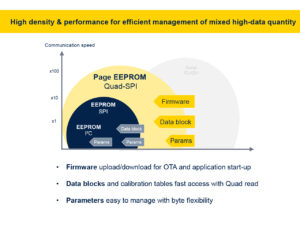 Understanding EEPROM
One of the main advantages of electrically erasable programmable read-only memory is its byte-level granularity. Whereas writing to other memory types, like flash, means erasing an entire sector, which can range from many bytes to hundreds of kilobytes, depending on the model, an EEPROM is writable byte by byte. This is tremendously beneficial when writing logs, sensor data, settings, and more, as it saves time, energy, and reduces complexity, since the writing operation requires fewer steps and no buffer. For instance, using an EEPROM can save significant resources and speed up manufacturing when updating a calibration table on the assembly line.
PerformanceThe very nature of EEPROM also gives it a significant endurance advantage. Whereas flash can only support read/write cycles in the hundreds of thousands, an EEPROM supports millions, and its data retention is in the hundreds of years, which is crucial when dealing with systems with a long lifespan. Similarly, its low peak current of a few milliamps and its fast boot time of 30 µs mean it can meet the most stringent low-power requirements. Additionally, it enables engineers to store and retrieve data outside the main storage. Hence, if teams are experiencing an issue with the microcontroller, they can extract information from the EEPROM, which provides additional layers of safety.
ConvenienceThese unique abilities explain why automotive, industrial, and many other applications just can’t give up EEPROM. For many, giving it up could break software implementation or require a significant redesign. Indeed, one of the main advantages of EEPROM is that they fit into a small 8-pin package regardless of memory density (from 1 Kbit to 32 Mbit). Additionally, they tolerate high operating temperatures of up to 145 °C for serial EEPROM, making them easy to use in a wide range of environments. The middleware governing their operations is also significantly more straightforward to write and maintain, given their operation.
ResilienceSince ST controls the entire manufacturing process, we can provide greater guarantees to customers facing supply chain uncertainties. Concretely, ST offers EEPROM customers a guarantee of supply availability through our longevity commitment program (10 years for industrial-grade products, 15 years for automotive-grade). This explains why, 40 years after EEPROM development began in 1985 and after two decades of leadership, some sectors continue to rely heavily on our EEPROMs. And why new customers seeking a stable long-term data storage solution are adopting it, bolstered by ST’s continuous innovations, enabling new use cases.
Why will the industry need EEPROM tomorrow? More storage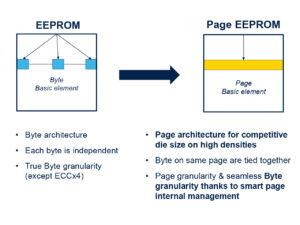 EEPROM vs. Page EEPROM
Since its inception in the late 70s, EEPROM’s storage has always been relatively minimal. In many instances, it is a positive feature for engineers who want to reserve their EEPROM for small, specific operations and segregate it from the rest of their storage pool. However, as serial EEPROM reached 4 Mbit and 110 nm, the industry wondered whether the memory could continue to grow in capacity while shrinking process nodes. A paper published in 2004 initially concluded that traditional EEPROMs “scale poorly with technology”. Yet, ST recently released a Page EEPROM capable of storing 32 Mbit that fits inside a tiny 8-pin package.
The Page EEPROM adopts a hybrid architecture, meaning it uses 16-byte words and 512-byte pages while retaining the ability to write at the byte level. This offers customers the flexibility and robustness of traditional EEPROM but bypasses some of the physical limitations of serial EEPROM, thus increasing storage and continuing to serve designs that rely on this type of memory while still improving endurance. Indeed, a Page EEPROM supports a cumulative one billion cycles across its entire memory capacity. For many, Page EEPROMs represent a technological breakthrough by significantly expanding data storage without changing the 8-pin package size. That’s why we’ve seen them in asset tracking applications and other IoT applications that run on batteries.
New featuresST also recently released a Unique ID serial EEPROM, which uses the inherent capabilities of electrically erasable programmable read-only memory to store a unique ID or serial number to trace a product throughout its assembly and life cycle. Usually, this would require additional components to ensure that the serial number cannot be changed or erased. However, thanks to its byte-level granularity and read-only approach, the new Unique ID EEPROM can store this serial number while preventing any changes, thus offering the benefits of a secure element while significantly reducing the bill of materials. Put simply, the future of EEPROM takes the shape of growing storage and new features.
The post 20 Years of EEPROM: Why It Matters, Needed, and Its Future appeared first on ELE Times.
Navitas unveils fifth-generation SiC Trench-Assisted Planar MOSFET technology
Modern Cars Will Contain 600 Million Lines of Code by 2027
Courtesy: Synopsys
The 1977 Oldsmobile Toronado was ahead of its time.
Featuring an electronic spark timing system that improved fuel economy, it was the first vehicle equipped with a microprocessor and embedded software. But it certainly wasn’t the last.
While the Toronado had a single electronic control unit (ECU) and thousands of lines of code (LOC), modern vehicles have many ECUs and 300 million LOC. What’s more, the pace and scale of innovation continue to accelerate at an exponential, almost unfathomable rate.
It took half a century for cars to reach 300 million LOC.
We predict the amount of software in vehicles will double in the next 12 months alone, reaching 600 million LOC or more by 2027.
The fusion of automotive hardware and software
Automotive design has historically been focused on structural and mechanical platforms — the chassis and engine. Discrete electronic and software components were introduced over time, first to replace existing functions (like manual window cranks) and later to add new features (like GPS navigation).
For decades, these electronics and the software that define them were designed and developed separately from the core vehicle architecture — standalone components added in the latter stages of manufacturing and assembly.
This approach is no longer viable.
Not with the increasing complexity and interdependence of automotive electronics. Not with the criticality of those electronics for vehicle operation, as well as driver and passenger safety. And not with a growing set of software-defined platforms — from advanced driver assistance (ADAS) and surround view camera systems to self-driving capabilities and even onboard agentic AI — poised to double the amount of LOC in vehicles over the next year.
From the chassis down to the code, tomorrow’s vehicles must be designed, developed, and tested as a single, tightly integrated, highly sophisticated system.
Shifting automotive business models
The rapid expansion of vehicular software isn’t just a technology trend — it’s rewriting the economics of the automotive industry. For more than a century, automakers competed on horsepower, handling, and mechanical innovation. Now, the battleground is shifting to software features, connectivity, and continuous improvement.
Instead of selling a static product, OEMs are adopting new, more dynamic business models where vehicles evolve long after they leave the showroom. Over-the-air updates can deliver new capabilities, performance enhancements, and safety improvements without a single trip to the dealer. And features that used to be locked behind trim levels can be offered as on-demand upgrades or subscription services.
This transition is already underway.
Some automakers are experimenting with monthly fees for heated seats or performance boosts. Others are building proprietary operating systems to replace third-party platforms, giving them control over the user experience — as well as the revenue stream. By the end of the decade, software subscriptions will become as common as extended warranties, generating billions in recurring revenue and fundamentally changing how consumers think about car ownership.
The engineering challenge behind OEM transformation
Delivering on the promise of software-defined vehicles (SDVs) that continuously evolve isn’t as simple as adding more code. It requires a fundamental rethinking of how cars are designed, engineered, and validated.
Hundreds of millions of lines of code must push data seamlessly across a variety of electronic components and systems. And those systems — responsible for sensing, safety, communication, and other functions — must work in concert with millisecond precision.
For years, vehicle architectures relied on dozens of discrete ECUs, each dedicated to a specific function. But as software complexity grows, automakers are shifting toward fewer, more powerful centralised compute platforms that can handle much larger workloads. This means more code is running on less hardware, with more functionality consolidated onto a handful of high-performance processors. As a result, the development challenge is shifting from traditional ECU integration — where each supplier delivered a boxed solution — to true software integration across a unified compute platform.
As such, hardware and software development practices can no longer be separate tracks that converge late in the process. They must be designed together and tailored for one another — well before any physical platform exists.
This is where electronics digital twins (eDTs) are becoming indispensable. By creating functionally accurate virtual models of vehicle electronics and systems, design teams can shift from late-stage integration to a model where software and hardware are co-developed from day one.
eDTs and virtual prototypes do more than enable earlier software development at the component level — they allow engineers to simulate, validate, and optimise the entire vehicle electronics. This means teams can see how data flows across subsystems, how critical components interact under real-world scenarios, and how emerging features might impact overall safety and performance. With eDTs, automakers can test billions — even trillions — of operating conditions and edge cases, many of which would be too costly, too time-consuming, or otherwise infeasible with physical prototypes.
By embracing eDTs, the industry is not just keeping pace with escalating complexity — it is re-engineering longstanding engineering processes, accelerating innovation, and improving the quality and safety of tomorrow’s vehicles.
The road ahead
Our prediction of cars containing 600 million lines of code by 2027 isn’t just a number. It signals a turning point for an industry that has operated in largely the same manner for more than a century.
Many automakers are reimagining their identity.
No longer just manufacturers, they’re becoming technology companies with business models that resemble those of cloud providers and app developers. They’re adopting agile, iterative practices, where updates roll out continuously rather than in multi-year product refreshes. And they’re learning how to design, develop, test, and evolve their products as a unified system — from chassis and engine to silicon and software — rather than a collection of pieces that are assembled on a production line.
Unlike the 1977 Oldsmobile Toronado, the car you buy in 2027 won’t be the same car you drive in 2030 — and that’s by design.
The post Modern Cars Will Contain 600 Million Lines of Code by 2027 appeared first on ELE Times.
Advancement in waveguides to progress XR displays, not GPUs
Across emerging technology domains, a familiar narrative keeps repeating itself. In Extended Reality (XR), progress is often framed as a race toward ever more powerful GPUs. In wireless research, especially around 6G, attention gravitates toward faster transistors and higher carrier frequencies in the terahertz (THz) regime. In both cases, this framing is misleading. The real constraint is no longer raw compute or device-level performance. It is system integration. This is not a subtle distinction. It is the difference between impressive laboratory demonstrations and deployable, scalable products.
XR Has Outgrown the GPU BottleneckIn XR, GPU capability has reached a point of diminishing returns as the primary limiter. Modern graphics pipelines, combined with foveated rendering, gaze prediction, reprojection, and cloud or edge offloading, can already deliver high-quality visual content within reasonable power envelopes. Compute efficiency continues to improve generation after generation. Yet XR has failed to transition from bulky headsets to lightweight, all-day wearable glasses. The reason lies elsewhere: optics, specifically waveguide-based near-eye displays.
Waveguides must inject, guide, and extract light with high efficiency while remaining thin, transparent, and manufacturable. They must preserve colour uniformity across wide fields of view, provide a sufficiently large eye-box, suppress stray light and ghosting, and operate at power levels compatible with eyewear-sized batteries. Today, no waveguide architecture geometric (reflective), diffractive, holographic, or hybrid solves all these constraints simultaneously. This reality leads to a clear conclusion: XR adoption will be determined by breakthroughs in waveguides, not GPUs. Rendering silicon is no longer the pacing factor; optical system maturity is.
The Same Structural Problem Appears in THz and 6GA strikingly similar pattern is emerging in terahertz communication research for 6G. On paper, THz promises extreme bandwidths, ultra-high data rates, and the ability to merge communication and sensing on a single platform. Laboratory demonstrations routinely showcase impressive performance metrics. But translating these demonstrations into real-world systems has proven far harder than anticipated. The question is no longer whether transistors can operate at THz frequencies; they can, but whether entire systems can function reliably, efficiently, and repeatably at those frequencies.
According to Vijay Muktamath, Founder of Sensesemi Technologies, the fundamental bottleneck holding THz radios back from commercialisation is system integration. Thermal management becomes fragile, clock and local oscillator integration grows complex, interconnect losses escalate, and packaging parasitics dominate performance. Each individual block may work well in isolation, but assembling them into a stable system is disproportionately difficult. This mirrors the XR waveguide challenge almost exactly.
When Integration Becomes Harder Than InnovationAt THz frequencies, integration challenges overwhelm traditional design assumptions. Power amplifiers generate heat that cannot be dissipated easily at such small scales. Clock distribution becomes sensitive to layout and material choices. Even millimetre-scale interconnects behave as lossy electromagnetic structures rather than simple wires.
As a result, the question of what truly limits THz systems shifts away from transistor speed or raw output power. Instead, the constraint becomes whether designers can co-optimise devices, interconnects, packaging, antennas, and thermal paths as a single electromagnetic system. In many cases, packaging and interconnect losses now degrade performance more severely than the active devices themselves. This marks a broader transition in engineering philosophy. Both XR optics and THz radios have crossed into a regime where system-level failures dominate component-level excellence.
Materials Are Necessary, But Not SufficientThis raises a critical issue for 6G hardware strategy: whether III–V semiconductor technologies such as InP and GaAs will remain mandatory for THz front ends. Today, their superior electron mobility and high-frequency performance make them indispensable for cutting-edge demonstrations.
However, relying exclusively on III–V technologies introduces challenges in cost, yield, and large-scale integration. CMOS and SiGe platforms, while inferior in peak device performance, offer advantages in integration density, manufacturability, and system-level scaling. Through architectural innovation, distributed amplification, and advanced packaging, these platforms are steadily pushing into higher frequency regimes. The most realistic future is not a single winner, but a heterogeneous architecture. III–V devices will remain essential where absolute performance is non-negotiable, while CMOS and SiGe handle integration-heavy functions such as beamforming, control, and signal processing. This mirrors how XR systems offload rendering, sensing, and perception tasks across specialised hardware blocks rather than relying on a single dominant processor.
Why THz Favours Point-to-Point, Not Cellular CoverageAnother misconception often attached to THz communication is its suitability for wide-area cellular access. While technically intriguing, this vision underestimates the physics involved. THz frequencies suffer from severe path loss, atmospheric absorption, and extreme sensitivity to blockage. Beam alignment overhead becomes significant, especially in mobile scenarios. As Mr Muktamath puts it, “THz is fundamentally happier in controlled environments. Point-to-point links, fixed geometries, short distances, that’s where it shines.”
THz excels in short-range, P2P links where geometry is controlled and alignment can be maintained. Fixed wireless backhauls; intra-data-centre communication, chip-to-chip links, and high-resolution sensing are far more realistic early applications. These use cases resemble the constrained environments where XR has found initial traction in enterprise, defence, and industrial deployments— rather than mass consumer adoption.
Packaging: The Silent DominatorPerhaps the clearest parallel between XR waveguides and THz radios lies in packaging. In XR, the waveguide itself is the package: it dictates efficiency, form factor, and user comfort. In THz systems, packaging and interconnects increasingly dictate whether the system works at all. Losses introduced by packaging can erase transistor-level gains. Thermal resistance can limit continuous operation. Antenna integration becomes inseparable from the RF front-end. This has forced a shift from chip- centric design to electromagnetic system design, where silicon, package, antenna, and enclosure are co-designed from the outset.
Communication and Sensing: Convergence with ConstraintsTHz also revives the idea of joint communication and sensing on shared hardware. In theory, high frequencies offer exceptional spatial resolution, making simultaneous data transmission and environmental sensing attractive. In practice, coexistence introduces non-trivial trade-offs.
Waveform design, dynamic range, calibration, and interference management all become more complex when reliability and throughput must be preserved. The most viable path is not full hardware unification, but carefully partitioned coexistence, with shared elements where feasible and isolation where necessary. This echoes XR architectures, where sensing and rendering share infrastructure but remain logically separated to maintain performance.
A Single Lesson Across Two DomainsXR waveguides and THz radios operate in different markets, but they are constrained by the same fundamental truth: the era of component-led innovation is giving way to system-led engineering. Faster GPUs do not solve optical inefficiencies. Faster transistors do not solve packaging losses, thermal bottlenecks, or integration fragility.
As Mr. Muktamath aptly concludes, “The future belongs to teams that can make complex systems behave simply, not to those who build the most impressive individual blocks.” The next generation of technology leadership will belong to organisations that master cross-domain co-design across devices, packaging, optics, and software. Manufacturability and yield as first-order design constraints, Thermal and power integrity as architectural drivers and Integration discipline over isolated optimisation. In both XR and THz, success will not come from building the fastest block, but from making the entire system work reliably, repeatedly, and at scale. That is the real frontier now.
The post Advancement in waveguides to progress XR displays, not GPUs appeared first on ELE Times.
AI-Enabled Failure Prediction in Power Electronics: EV Chargers, Inverters, and SMPS
Reliability is now a defining parameter for modern power electronic systems. As the world pushes harder toward electric mobility, renewable energy adoption, and high-efficiency digital infrastructure, key converters like EV chargers, solar inverters, and SMPS are running in incredibly demanding environments. High switching frequencies, aggressive power densities, wide bandgap materials (like SiC/GaN), and really stringent uptime expectations have all squeezed those reliability margins down to almost nothing. Clearly, traditional threshold-based alarms or basic periodic maintenance are no longer enough to guarantee stable operation.
This is exactly where AI-enabled failure prediction emerges as a breakthrough. By integrating real-time sensing, historical stress patterns, physics-based models, and deep learning, AI unlocks the ability to spot early degradation. This gives us the power to accurately estimate remaining useful life (RUL) and prevent catastrophic breakdowns long before they ever occur.
Jean‑Marc Chéry, CEO of STMicroelectronics, has emphasised that the practical value of AI in power electronics emerges at fleet and lifecycle scale rather than at individual-unit prediction level, particularly for SiC- and GaN-based SMPS.
Aggregated field data across large deployments is used to refine derating guidelines, validate device-level reliability models, and harden next-generation power technologies, instead of attempting deterministic failure prediction on a per-unit basis.
Limitations of Traditional Monitoring in Power Electronics
Conventional condition monitoring methods, things like simple temperature alarms, current protection limits, or basic event logs, operate reactively. They only catch failures after components have already drifted past the acceptable redline. Yet, converter failures actually start much earlier from subtle, long-term changes. Think about:
- Gradual ESR (Equivalent Series Resistance) increase in electrolytic capacitors
- Bond wire fatigue and solder joint cracking inside IGBT/MOSFET modules
- Gate oxide degradation in newer SiC devices
- Magnetic core saturation and insulation ageing
- Switching waveform distortions caused by gate driver drift
AI Techniques Powering Predictive Failure Intelligence
AI-based diagnostics in power electronics rest on three complementary pillars:
- Deep Learning for Real-Time Telemetry
AI-based diagnostics in power electronics rely on three complementary pillars:
Deep Learning for Real Time Telemetry Converters pump out rich telemetry data: temperatures, currents, switching waveforms, harmonics, soft switching behaviour, and acoustic profiles. Deep learning models find patterns here that are absolutely impossible for a human to spot manually.
- CNNs (Convolutional Neural Networks): These analyse switching waveforms, spot irregularities in turn-on/turn-off cycles, identify diode recovery anomalies, and classify abnormal transient events instantly.
- LSTMs (Long Short Term Memory Networks): These track the long-term drift in junction temperature, capacitor ESR, cooling efficiency, and load cycle behaviour over months.
- Autoencoders: learn the “healthy signature” of a converter and identify deviations that signal emerging faults.
- Physics-Informed ML
Pure machine learning struggles with operating points it has not seen; physics-informed machine learning offers better generalisation. It integrates:
- Power cycle fatigue equations
- MOSFET/IGBT thermal models
- Magnetics core loss equations
- Capacitor degradation curves
- SiC/GaN stress lifetime relationships
Peter Herweck, former CEO of Schneider Electric, has underscored that long-life power conversion systems cannot rely on data-driven models alone.
In solar and industrial inverters, Schneider Electric’s analytics explicitly anchor AI models to thermal behaviour, power-cycling limits, and component ageing physics, enabling explainable and stable Remaining Useful Life estimation across wide operating conditions.
- Digital Twins & Edge AI
Digital twins act as virtual replicas of converters, simulating electrical, thermal, and switching behaviour in real time. AI continuously updates the twin using field data, enabling:
- Dynamic stress tracking
- Load-cycle-based lifetime modelling
- Real-time deviation analysis
- Autonomous derating or protective responses
Edge-AI processors integrated into chargers, inverters, or SMPS enable on-device inference even without cloud connectivity.
AI-Driven Failure Prediction in EV Chargers
EV fast chargers (50 kW–350 kW+) operate under harsh conditions with high thermal and electrical stress. Uptime dictates consumer satisfaction, making predictive maintenance critical.
Key components under AI surveillance
- SiC/Si MOSFETs and diodes
- Gate drivers and isolation circuitry
- DC-link electrolytic and film capacitors
- Liquid/air-cooling systems
- EMI filters, contactors, and magnetic components
Roland Busch, CEO of Siemens, has emphasised that reliability in power-electronic infrastructure depends on predictive condition insight rather than reactive protection.
In high-power EV chargers and grid-connected converters, Siemens’ AI-assisted monitoring focuses on detecting long-term degradation trends—thermal cycling stress, semiconductor wear-out, and DC-link capacitor ageing—well before protection thresholds are reached.
AI-enabled predictive insights
- Waveform analytics: CNNs detect micro-oscillations in switching transitions, indicating gate driver degradation.
- Thermal drift modelling: LSTMs predict MOSFET junction temperature rise under high-power cycling.
- Cooling system performance: Autoencoders identify airflow degradation, pump wear, or radiator clogging.
- Power-module stress estimation: Digital twins estimate cumulative thermal fatigue and RUL.
Charging network operators report a 20–40% reduction in unexpected downtime by implementing AI-enabled diagnostics.
Solar & Industrial Inverters: Long-Life Systems Under Environmental Stress
Solar inverters operate for 10–20 years in harsh outdoor conditions—dust, high humidity, temperature cycling, and fluctuating PV generation.
Common failure patterns identified by AI
- Bond-wire lift-off in IGBT modules due to repetitive thermal stress
- Capacitor ESR drift affecting DC-link stability
- Transformer insulation degradation
- MPPT (Maximum Power Point Tracking) anomalies due to sensor faults
- Resonance shifts in LCL filters
AI-powered diagnostic improvements
- Digital twin comparisons highlight deviations in thermal behaviour or DC-link ripple.
- LSTM RUL estimation predicts when capacitors or IGBTs are nearing end-of-life.
- Anomaly detection identifies non-obvious behavior such as partial shading impacts or harmonic anomalies.
SMPS: High-Volume Applications Where Reliability Drives Cost Savings
SMPS units power everything from telecom towers to consumer electronics. With millions of units deployed, even a fractional improvement in reliability creates massive financial savings.
AI monitors key SMPS symptoms
- Switching frequency drift due to ageing components
- Hotspot formation on magnetics
- Acoustic signatures of transformer failures
- Leakage or gate-charge changes in GaN devices
- Capacitor health degradation trends
Manufacturers use aggregated fleet data to continuously refine design parameters, enhancing long-term reliability.
Cross-Industry Benefits of AI-Enabled Failure Prediction
Industries implementing AI-based diagnostics report:
- 30–50% reduction in catastrophic failures
- 25–35% longer equipment lifespan
- 20–30% decline in maintenance expenditure
- Higher uptime and service availability
Challenges and Research Directions
Even with significant progress, several challenges persist:
- Scarcity of real-world failure data: Failures occur infrequently; synthetic data and stress testing are used to enrich datasets.
- Model transferability limits: Variations in topology, gate drivers, and cooling systems hinder direct model reuse.
- Edge compute constraints: Deep models often require compression and pruning for deployment.
- Explainability requirements: Engineers need interpretable insights, not just anomaly flags.
Research in XAI, transfer learning, and physics-guided datasets is rapidly addressing these concerns.
The Future: Power Electronics Designed with Built-In Intelligence
In the coming decade, AI will not merely monitor power electronic systems—it will actively participate in their operation:
- AI-adaptive gate drivers adjusting switching profiles in real time
- Autonomous derating strategies extending lifespan during high-stress events
- Self-healing converters recalibrating to minimise thermal hotspots
- Cloud-connected fleet dashboards providing RUL estimates for entire EV charging or inverter networks
- WBG-specific failure prediction models tailored for SiC/GaN devices
Conclusion
AI-enabled failure prediction is completely transforming the reliability of EV chargers, solar inverters, and SMPS systems. Engineers are now integrating sensor intelligence, deep learning, physics-based models, and digital twin technology. This allows them to spot early degradation, accurately forecast future failures, and effectively stretch the lifespan of the equipment.
This whole predictive ecosystem doesn’t just cut your operational cost; it significantly boosts system safety, availability, and overall performance. As electrification accelerates, AI-driven reliability will become the core foundation of next-generation power electronic design. It makes systems smarter, more resilient, and truly future-ready.
The post AI-Enabled Failure Prediction in Power Electronics: EV Chargers, Inverters, and SMPS appeared first on ELE Times.
📰 Газета "Київський політехнік" № 5-6 за 2026 (.pdf)
")
Вийшов 5-6 номер газети "Київський політехнік" за 2026 рік
Powering AI: How Power Pulsation Buffers are transforming data center power architecture
Courtesy: Infineon Technologies
Microsoft, OpenAI, Google, Amazon, NVIDIA, etc. are racing against each other, and it is for good reasons: to build massive data centres with billions of dollars in investments.
Imagine a data centre humming with thousands of AI GPUs, each demanding bursts of power like a Formula 1 car accelerating out of a corner. Now imagine trying to feed that power without blowing out the grid.
That is the challenge modern AI server racks face, and Infineon’s Power Pulsation Buffer (PPB) might just be the pit crew solution you need.
Why AI server power supply needs a rethink
As artificial intelligence continues to scale, so does the power appetite of data centres. Tech giants are building AI clusters that push rack power levels beyond 1 MW. These AI PSUs (power supply units) are not just hungry. They are unpredictable, with GPUs demanding sudden spikes in power that traditional grid infrastructure struggles to handle.
These spikes, or peak power events, can cause serious stress on the grid, especially when multiple GPUs fire up simultaneously. The result? Voltage drops, current overshoots, and a grid scrambling to keep up.
 Figure 1: Example peak power profile demanded by AI GPUs
Rethinking PSU architecture for AI racks
To tackle this, next-gen server racks are evolving. Enter the power sidecar, a dedicated module housing PSUs, battery backup units (BBUs), and capacitor backup units (CBUs). This setup separates power components from IT components, allowing racks to scale up to 1.3 MW.
But CBUs, while effective, come with trade-offs:
- Require extra shelf space
- Need communication with PSU shelves
- Add complexity to the rack design
This is where PPBs come in.
What is a Power Pulsation Buffer?
Think of PPB as a smart energy sponge. It sits between the PFC voltage controller and the DC-DC converter inside the PSU, soaking up energy during idle times and releasing it during peak loads. This smooths out power demands and keeps the grid happy.
PPBs can be integrated directly into single-phase or three-phase PSUs, eliminating the need for bulky CBUs. They use SiC bridge circuits rated up to 1200 V and can be configured in 2-level or 3-level designs, either in series or parallel.
PPB vs. traditional PSU
In simulations comparing traditional PSUs with PPB-enhanced designs, the difference is striking. Without PPB, the grid sees a sharp current overshoot during peak load. With PPB, the PSU handles the surge internally, keeping grid power limited to just 110% of rated capacity.
This means:
- Reduced grid stress
- Stable input/output voltages
Better energy utilisation from PSU bulk capacitors
 Figure 3: Simulation of peak load event: Without PPB (left) and with PPB (right) in 3-ph HVDC PSU
PPB operation modes
PPBs operate in two modes, on-demand and continuous. Each is suited to different rack designs and power profiles.
- On-demand operation: Activates only during peak events, making it ideal for short bursts. It minimises energy loss and avoids unnecessary grid frequency cancellation
- Continuous operation: By contrast, always keeps the PPB active. This supports steady-state load jumps and enables DCX with fixed frequency, which is especially beneficial for 1-phase PSUs.
Choosing the right mode depends on the specific power dynamics of your setup.
Why PPB is a game-changer for AI infrastructure
PPBs are transforming AI server power supply design. They manage peak power without grid overload and integrate compactly into existing PSU architectures.
By enhancing energy buffer circuit performance and optimising bulk capacitor utilisation, PPBs enable scalable designs for high-voltage DC and 3-phase PSU setups.
Whether you are building hyperscale data centres or edge AI clusters, PPBs offer a smarter, grid-friendly solution for modern power demands.
The post Powering AI: How Power Pulsation Buffers are transforming data center power architecture appeared first on ELE Times.
AI-powered MCU elevates vehicle intelligence

The Stellar P3E automotive MCU from ST features built-in AI acceleration, enabling real-time AI applications at the edge. Designed for the next generation of software-defined vehicles, it simplifies multifunction integration, supporting X-in-1 electronic control units from hybrid/EV systems to body zonal architectures.

According to ST, the Stellar P3E is the first automotive MCU with an embedded neural network accelerator. Its Neural-ART accelerator, a dedicated neural processing unit (NPU) with an advanced data-flow architecture, offloads AI workloads from the main cores, speeding up inference execution and delivering real-time, AI-based virtual sensing.
The MCU incorporates 500-MHz Arm Cortex-R52+ cores, delivering a CoreMark score exceeding 8000 points. Its split-lock feature lets designers balance functional safety with peak performance, while smart low-power modes go beyond conventional standby. The device also includes extensible xMemory, with up to twice the density of standard embedded flash, plus rich I/O interfaces optimized for advanced motor control.
Stellar P3E production is scheduled to begin in the fourth quarter of 2026.
The post AI-powered MCU elevates vehicle intelligence appeared first on EDN.
Gate drivers emulate optocoupler inputs

Single-channel isolated gate drivers in the 1ED301xMC121 series from Infineon are pin-compatible replacements for optocoupler-based designs. They replicate optocoupler input characteristics, enabling drop-in use without control circuit changes, while using non-optical isolation internally to deliver higher CMTI and improved switching performance for SiC applications.

Their opto-emulator input stage uses two pins and integrates reverse voltage blocking, forward voltage clamping, and an isolated signal transmitter. With CMTI exceeding 300 kV/µs, 40-ns propagation delay, and 10-ns part-to-part matching, the devices deliver robust, high-speed switching performance.
The series includes three variants—1ED3010, 1ED3011, and 1ED3012—supporting Si and SiC MOSFETs as well as IGBTs. Each delivers up to 6.5 A of output current to drive power modules and parallel switch configurations in motor drives, solar inverters, EV chargers, and energy storage systems. The drivers differ in UVLO thresholds: 8.5 V, 11 V, and 12.5 V for the 1ED3010, 1ED3011, and 1ED3012, respectively.
The 1ED3010MC121, 1ED3011MC121, and 1ED3012MC121 drivers are available in CTI 600, 6-pin DSO packages with more than 8 mm of creepage and clearance.
The post Gate drivers emulate optocoupler inputs appeared first on EDN.
IC enables precise current sensing in fast control loops

Allegro Microsystems’ ACS37017 Hall-effect current sensor achieves 0.55% typical sensitivity error across temperature and lifetime. High accuracy, a 750‑kHz bandwidth, and a 1‑µs typical response time make the ACS37017 suitable for demanding control loops in automotive and industrial high-voltage power conversion.

Unlike conventional sensors whose accuracy suffers from drift, the ACS37017 delivers long-term stability through a proprietary compensation architecture. This technology maintains precise measurements, ensuring control loops remain stable and efficient throughout the operating life of the vehicle or power supply.
The ACS37017 features an integrated non-ratiometric voltage reference, simplifying system architecture by eliminating the need for external precision reference components. This integration reduces BOM costs, saves board space, and removes a major source of system-level noise and error.
The high-accuracy ACS37017 expands Allegro’s current sensor portfolio, complementing the ACS37100 (optimized for speed) and the ACS37200 (optimized for power density). Request the preliminary datasheet and engineering samples on the product page linked below.
The post IC enables precise current sensing in fast control loops appeared first on EDN.
Microchip empowers real-time edge AI

Microchip provides a full-stack edge AI platform for developing and deploying production-ready applications on its MCUs and MPUs. These devices operate at the network edge, close to sensors and actuators, enabling deterministic, real-time decision-making. Processing data locally within embedded systems reduces latency and improves security by limiting cloud connectivity.

The full-stack application portfolio includes pretrained, production-ready models and application code that can be modified, extended, and deployed across target environments. Development and optimization are performed using Microchip’s embedded software and ML toolchains, as well as partner ecosystem tools. Edge AI applications include:
- AI-based detection and classification of electrical arc faults using signal analysis
- Condition monitoring and equipment health assessment for predictive maintenance
- On-device facial recognition with liveness detection for secure identity verification
- Keyword spotting for consumer, industrial, and automotive command-and-control interfaces
Microchip is working with customers deploying its edge AI solutions, providing model training guidance and workflow integration across the development cycle. The company is also collaborating with ecosystem partners to expand available software and deployment options. For more information, visit the Microchip Edge AI page.
The post Microchip empowers real-time edge AI appeared first on EDN.
AI agent automates front-end chip workflows

Cadence has launched the ChipStack AI Super Agent, an agentic AI solution for front-end silicon design and verification. The platform automates key design and test workflows—including coding, test plan creation, regression testing, debugging, and issue resolution—offering significant productivity gains for chip development teams. It leverages multiple AI agents that work alongside Cadence’s existing EDA tools and AI-based optimization solutions.

The ChipStack AI Super Agent supports both cloud-based and on-premises AI models, including NVIDIA NeMo models that can be customized for specific workflows, as well as OpenAI GPT. By combining agentic AI orchestration with established simulation, verification, and AI-assistant tools, the platform streamlines complex semiconductor workflows.
Early deployments at leading semiconductor companies have demonstrated measurable reductions in verification time and improvements in workflow efficiency. The platform is currently available in early access for customers looking to integrate AI-driven automation into front-end chip design and verification processes.
Additional information about the ChipStack AI Super Agent can be found on the Cadence AI for Design page.
The post AI agent automates front-end chip workflows appeared first on EDN.
Сторінки


![[link]](https://i.redd.it/v6u4b0ql4kjg1.jpeg)