
Збирач потоків
Government’s Green Signal to 22 projects under ECMS
The Ministry of Electronics and IT has supposedly approved 22 new projects under the Electronics Components’ Manufacturing Scheme on January 02, 2026, with a projected investment of ₹41,863 crore and production of ₹2,58,152 crore.
The said proposals include those from Dixon, Samsung Display Noida Pvt Ltd, Foxconn (Yuzhan Technology India Pvt Ltd), and Hindalco Industries. These are expected to provide nearly 33,791 direct employment opportunities. This approval comes after the Ministry approved 24 proposals under the ECMS earlier.
The approval letters were handed directly by Union Minister Ashwini Vaishnav to those part of the above 22 projects on Friday.
As per a background note circulated by the Ministry on the third tranche of approvals, the nod includes the manufacturing of 11 target segment products that have cross-sectoral applications, such as mobile manufacturing, telecom, consumer electronics, strategic electronics, automotive, and IT hardware.
Of 11 products, 5 are bare components such as PCBs, Capacitors, Connectors, Enclosures, and Li-ion Cells; 3 pertain to sub-assemblies such as Camera Modules, Display Modules, and Optical Transceivers; and 3 are supply chain items such as Aluminium Extrusion, Anode Material, and Laminate.
The background note said the approvals aim to significantly strengthen domestic supply chains, reduce import dependence for critical electronic components, and support the growth of high-value manufacturing capabilities in India.
The post Government’s Green Signal to 22 projects under ECMS appeared first on ELE Times.
Beyond technology: ST’s commitment to educating and inspiring next generation
ST is well known as a global company creating technology and driving innovation. But it’s not just that. Its role extends beyond manufacturing products: the company is committed to inspiring and educating future generations by supporting scientific research, STEM initiatives, and engaging in talent development. This article provides an overview of ST’s recent and ongoing educational activities across key regions, including Italy, France, Singapore, and the United States.
Activities Across STEM, university relations and talent developmentST maintains a strong presence in the communities where it operates, participating in local and national events. Through various initiatives, the company connects with a broad spectrum of audiences, from primary and secondary school students and university graduates to experienced researchers. This commitment is further amplified through the ST Foundation, which leverages technology and education to drive social progress, promoting digital inclusion for disadvantaged communities globally. Regardless of the audience’s level of expertise, ST’s goal remains the same: promoting scientific culture and making the complex processes that lead to the production of our chips understandable.
Recent educational events in ItalyIn Italy, ST organises more than 200 events annually, reaching approximately 18,000 students ranging from preschool to high school and university. Below are some of the key initiatives we’ve recently organised.
Neapolis Innovation Summer Campus Participants at Neapolis Innovation Summer Campus
Between late August and early September, the ST site in Arzano (Naples) hosted the twelfth edition of the Neapolis Innovation Summer Campus in collaboration with five universities in Campania. This annual ten-day training program is intended for bachelor’s and master’s degree students who want to explore the use of 32-bit microcontroller platforms and seek an opportunity to interact with industry experts. The initiative offered intensive, hands-on seminars at the ST site and provided a kit of components for the project work that students presented at the end of the event. Additionally, the event hosted small and medium enterprises and start-ups throughout its entire duration, allowing them to present themselves and build connections with young talent.
Researchers’ Night in MilanIn September 2025, ST took part in the Researchers’ Night in Milan, an event promoted by the European Commission as part of the Marie Skłodowska-Curie Actions, hosting research centres, institutions, universities, and organisations engaged in scientific dissemination. ST showcased its Edge AI technology: one of the demos included the LSM6DSV80X sensor with the STEVAL-MKI247A board, connected to the SensorTile.box PRO, and demonstrated how to monitor high-impact activities in soccer (for example, between the player’s shoe and the ball) and collect valuable information for game analysis.
Maker Faire Rome – European Edition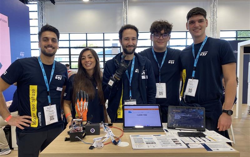 The STEM student winners of the 12th edition of the Neapolis Innovation Summer Campus 2025 with the smart glove “Hermes’ Hand”.
We also participated in Maker Faire Rome – European edition. This annual event has a varied audience, from school to university students, to startups, companies, and government institutions. Visitors could interact with demos in different fields, such as electronics, augmented reality, artificial intelligence, robotics, gaming, music and art. ST organised workshops covering Edge AI, robotics, and the STM32 Open Development Environment. A highlight was the “Hermes’ Hand”, a smart glove developed by a STEM student of the 12th edition of the Neapolis Innovation Summer Campus 2025. This project uses the STM32G474RE, X-NUCLEO-IKS4A1, and custom-made MEMS sensors to translate one’s voice into sign language in real time, breaking down communication barriers.
Science Festival in Genoa The “magic” wand demo
Another event held at the end of 2025 and aimed primarily at young students and families was the Science Festival in Genoa. ST presented “AI in your hands”: a magic wand, waved by visitors, demonstrated how the Integrated Signal Processing Unit (ISPU) in MEMS sensors can process movement locally (at the edge). Limited dependence on the cloud ensures high response speed, low power consumption, and greater security. Behind the playfulness and the visitors’ amazement, therefore, there was not magic but rather powerful local data processing.
Agreement with Polytechnic University of Turin
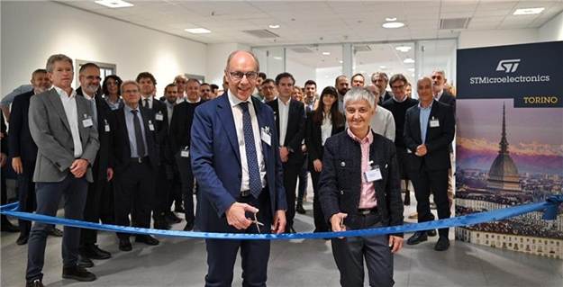 Inauguration of ST’s new design centre at the Polytechnic University of Turin. In the picture, Pro-Rector Elena Baralis and CEO of STMicroelectronics Italy Alberto Della Chiesa
To strengthen its ties with universities, in October, ST and the Polytechnic University of Turin renewed their framework agreement for the next four years and celebrated the inauguration of a new ST design centre space. The collaboration focuses on research and training of undergraduate and graduate students, particularly in fast-evolving fields such as cybersecurity, AI, and energy efficiency. Since 2019, STMicroelectronics has hired over 200 graduates (bachelor’s, master’s, and doctoral degrees) from the Polytechnic University of Turin. Many undergraduate and graduate students also work on their theses with the help of ST employees at the Turin centre.
Educational initiatives in FranceIn France, there is a virtuous example showing how recruitment needs in the field of microelectronics can favour high-level training for students and professionals. ST is one of the actors in the I-NOVMICRO program, a consortium of different companies that promotes microelectronics and electronics careers and provides advanced training in the Southern French Region (Rousset, Toulon, Sophia-Antipolis).
 Participants at I-NOVGAME
Launched in 2019, this initiative directly addresses recruitment needs by offering specialised training that qualifies people for technical sectors, particularly manufacturing jobs. Since the beginning of the project, more than 15,000 people have been trained, from secondary schools to baccalaureate level. This program allows students to learn semiconductor manufacturing processes in real-world conditions: facilities include an educational clean room and an educational grey room dedicated to maintenance training. The program also finances and leads a network of 12 Fab Labs in local high schools, coordinated by ST Rousset, and promotes STEM disciplines through school visits. The project’s ambition is to reach out all the whole of France and then expand on a European scale.
I-NOVMICRO also includes:
- I-NOVGAMES, an STM32 engineering and application challenge involving six engineering schools.
- INNOV ISLAND, a dynamic Metaverse offering a digital and 3D environment for training, educational materials, conferences, and job dating for students and employees.
Beyond direct training, ST supports education through donations of unused laboratory equipment, computers and STM32 microcontroller boards every year to schools and partners. Our company also offers career guidance through diverse programs and initiatives, primarily focused on engaging young people and supporting students with disabilities:
- For industrie, l’Univers Extraordinaire is a digital educational event which presents industry professions to young people through video game formats. ST participation includes virtual tours of ST facilities, video interviews with Rousset employees, and live presentations by industry professionals.
- Programs for students with disabilities at the Rousset site. Voyage au cœur de l’entreprise (VACLE) allows eight pupils to explore a dozen different professions over the course of a week, while Mentorat au coeur de l’entreprise (MACLE) is a mentorship program for high school students, where volunteer employees support students throughout their academic career, helping them plan their future, understand corporate culture, and develop their soft skills.
 On the left, participants at For industrie. On the right, a videogame screenshot.
Open-source and hands-on education with universities and partners in the US
On the left, participants at For industrie. On the right, a videogame screenshot.
Open-source and hands-on education with universities and partners in the US
ST products and solutions can be useful for developing open-source programs. In the United States, for example, ST contributes to research and education by developing open-source curricula with a strong emphasis on hands-on learning. Professors at the universities we collaborate with (including MIT, UCLA, UC Berkeley, Rensselaer Polytechnic Institute, UC Santa Cruz, and Santa Clara University) use ST development tools, such as the popular STM32 microcontroller platform, in their courses, which are then publicly available on our website. One main area of development now is to adapt the existing curricula to the AI era, which is strongly affecting the job market and how students interact with hardware and firmware programming. For this reason, ST is working with organisations like the MIT CSAIL Alliances (Computer Science and Artificial Intelligence Laboratory) on research, particularly regarding AI computing on devices at the edge and applications in robotics.
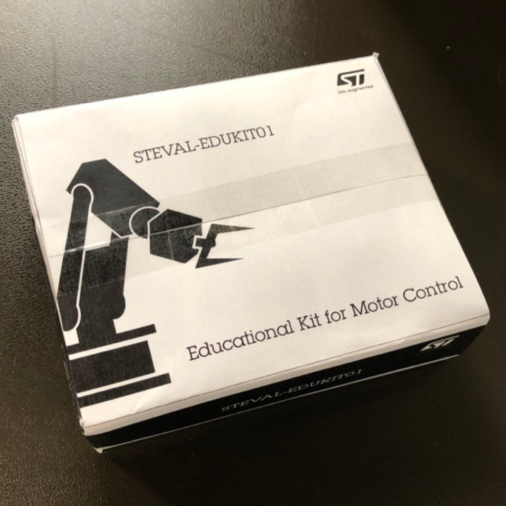 The STEVAL-EDUKIT01
Furthermore, we collaborate with partners who share our vision. With ARM, we have formed an Educational Alliance to support new curricula that will help students gain the necessary skills to become the professionals of the future. Some of these programs were developed in collaboration with the university and published on EdX, reaching over 40,000 enrollments over a four-year period. ST, SparkFun (member of ST Partner Program), DEKA and the Worcester Institute of Technology developed the Experiential Robotics Platform (XRP), an open-source platform for STEM education. Among other things, the XRP is the main provider of educational kits for the FIRST Robotics Competition, the largest STEM competition in the world, which targets primary and secondary schools and registered 785,000 participants in the 2024-25 school year.
Educational initiatives have helped ST products become among the most popular educational products in the United States. The STEVAL-EDUKIT01, developed in collaboration with UCLA, is the first ST development kit designed specifically for education and offers teaching materials for motor control and control systems.
Skills development and positive social impact in Singapore Participants at the STEM Fest organised by United Women Singapore
In Singapore, ST is adopting an educational approach that spans the entire learning journey, from primary schools to higher education. The goal is to drive a positive social impact and bridge the skills gap in semiconductor manufacturing by aligning education with industry needs. This comprehensive approach also focuses on inclusion addressing gender imbalance in the industry. To this end, ST partners with the United Women Singapore (UWS) to implement STEM initiatives for girls, such as the UWS STEM Fest. These initiatives provide mentorship, coaching, and networking to encourage more women to pursue STEM careers. Furthermore, ST fosters creativity and social responsibility in partnership with the Singapore Institute of Technology through the SIT Community Challenge. This program challenges students to develop sustainable technology solutions addressing real-world community issues such as urban mobility and environmental sustainability, directly supporting Singapore’s Smart Nation goals.
ST collaborates with Universities like the Singapore Institute of Technology (SIT) and the Institute of Technical Education (ITE). Our company develops and reviews curricula in microelectronics and semiconductor manufacturing through faculty exchange programs, ST guest lectures and participation in academic advisory committees to ensure relevance to industry demands. Additionally, ST provides practical experience through extensive vocational training, including the Integrated Work-Study Program (IWSP) in collaboration with SIT and Work-Study Diplomas (WSDip) offered by ITE, which provide students with up to 12 months and two years, respectively, of internship experience alongside ST professionals.
ST also invests in future talents through scholarships, including the Singapore Industry Scholarships (SgIS) and the Engineering and Tech Programme Scholarship (ETPS), which support students from pre-university through tertiary education. The flagship STICan (ST I Can) Work Experience Program (WEP) offers students aged 15 to 22 internships across the semiconductor value chain, from R&D and chip design to wafer fabrication and marketing. The program provides technical exposure and personal development courses to prepare students for university and careers.
ConclusionST’s engagement in educational and STEM activities serves a dual purpose: cultivating the next generation of talent while contributing to societal progress. From university partnerships to global outreach events, these initiatives form the foundation of ST’s commitment to driving innovation and developing technology responsibly for the future.
The post Beyond technology: ST’s commitment to educating and inspiring next generation appeared first on ELE Times.
https://www.semiconductor-today.com/news_items/2026/jan/tclcsot-prima-020126.shtml
How 2025’s Constraints Became the Blueprint for Electronics System Design in 2026?
As the electronics industry looks back at 2025, a clear shift toward efficiency, miniaturisation, and—most critically—more deliberate material choices becomes evident. The year stands out as a pivotal phase in the evolution of electronics, enabling systems tailored to the increasingly demanding requirements of data centres, advanced sensing platforms, electrified systems, and next-generation semiconductor packaging. Rather than chasing raw performance, the industry in 2025 was forced to reconcile ambition with practicality—balancing sustainability goals, high-performance demands, and mounting geopolitical pressures.
Escalating power densities driven by AI-centric data centers and electrification, shrinking thermal headroom resulting from aggressive miniaturization and higher levels of integration, and growing material availability constraints shaped by geopolitics and post–Moore’s Law design dependencies collectively emerged as defining parameters in the system architectures of automotive, industrial, and infrastructure electronics.
“Performance scaling today is increasingly driven by materials-centric advanced packaging,” says Suraj Rengarajan, Head of Semiconductor Product Group, Applied Materials India. As the industry enters a new year, these forces offer a clear lens through which to examine the design choices and innovations that defined electronics in 2025. Further, to give a better idea of how electrical design is changing in its basics, Suraj from Applied Materials India adds that System-level power, performance, area, and cost are now set by co-optimizing the bonding interface, low‑k dielectrics, redistribution-layer etch, barrier/seed, copper fill, and CMP, and thermal interfaces, treating interconnect resistance and heat flux as primary design variables.
In every aspect that we will be examining in the course of our story, we will try and see how the new dynamics of the industry shaped the preferences of the design engineers to sustain the innovations and applications, including data centres, automotives, and industrial applications.
Power Efficiency over Capability!
As the electrification phenomenon rapidly spread its wings, power efficiency, and not power capacity, became the primary constraint. As the demand across the sectors increased, it raised the energy demands significantly while simultaneously tightening thermal and sustainability limits. This realisation brought the power electronics landscape into the core architectural consideration of an electrical design engineer. In such a condition, the industry moved to significantly increase the power handled per unit area- Power Density.
With AI workloads driving processor currents from a few hundred amperes to well over a thousand—without any meaningful increase in board or package footprint—power efficiency emerged as the only viable path to sustain compute scaling.
This enabled the engineers to focus on more basic and intrinsic aspects of power electronics, which as efficiency, facilitating the same at every level of electronics design. To sustain the new dynamic, the industry moved towards Wide Band-gap (WBG) technologies, including Silicon Carbide (SiC) & Gallium Nitride (GaN). This helped the engineers to prevent switching and conduction losses along with heat generation per unit area, while abiding by tighter thermal and packaging constraints. The WBG technology also pushed the efficiency of the electronic product significantly at the system level.
As power density increased, thermal removal became progressively harder, creating a self-reinforcing loop in which higher efficiency was required simply to preserve thermal headroom rather than to improve performance.
Application
In data centres, rising compute density is driving demand for compact, high-efficiency power solutions. Gallium nitride–based power supplies are gaining traction by improving efficiency, enabling higher switching frequencies, shrinking passive components, and reducing cooling needs. In some architectures, GaN also allows simplified or single-stage power conversion, lowering losses and bill-of-materials complexity while supporting higher voltages closer to the point of load.
“With AI workloads, processor current levels have scaled from a few hundred amperes to over a thousand amperes, while the physical footprint has remained largely unchanged. This has fundamentally pushed power density and efficiency to the centre of system design,” says Dr Kaushik Basu, Associate Professor at IISC Bangalore.
Thermal Limits Over Advanced Cooling
As power efficiency improvements enabled higher power densities, overall heat generation continued to rise—driven by increasing absolute power levels and the closer packing of heat sources within shrinking form factors. Under these conditions, heat was generated faster than it could be spread or dissipated, leading to steeper thermal gradients that placed greater stress on materials, interconnects, and interfaces. At the same time, as electronics moved toward more miniaturised, efficient, and reliability-critical designs, the cost, complexity, and reliability penalties associated with ever-more advanced cooling solutions became increasingly prohibitive.
“As power density increases, heat removal becomes increasingly difficult. That is why efficiency is no longer optional—there is simply no thermal headroom to absorb losses,” says Dr Basu. By 2025, the industry reached a clear realisation: cooling complexity could no longer scale indefinitely to offset rising power density. This marked a fundamental shift in design philosophy, with heat dissipation moving from a downstream mechanical consideration to a primary architectural constraint addressed early in the design cycle. “Designers are increasingly treating materials as first-class design parameters. For advanced nodes, device physics is fundamentally materials physics, ” says Suraj from Applied Materials India.
The growing adoption of advanced packaging approaches, including 2.5D and 3D packaging, was driven as much by electrical constraints as thermal ones, as rising currents made long power-delivery paths increasingly untenable due to conduction losses and localized heating. It emerged as the first line of defence against thermal stress, playing a critical role in protecting silicon devices while enabling higher levels of integration and system efficiency. Particularly, in vertically stacked 3D architectures, where multiple dies are interconnected using through-silicon vias (TSVs), thermal challenges become particularly acute due to limited heat escape paths and the formation of localised hotspots.
In such configurations, traditional air- or liquid-based cooling, or the addition of increasingly sophisticated cooling hardware, often proved insufficient, expensive, or impractical—especially in automotive, industrial, and infrastructure applications with stringent reliability and lifetime requirements. While advanced packaging shortened interconnect paths and reduced resistive losses, it also concentrated heat generation within smaller volumes, making thermal constraints more visible rather than eliminating them. “Teams now co‑simulate variability and reliability, electromigration, bias temperature instability, and time‑dependent dielectric breakdown, at the materials level alongside logic and layout,” says Suraj. As a result, thermal-aware system architecture and packaging design became indispensable in sustaining performance and reliability.
“Advanced packaging approaches such as 2.5D and 3D integration are largely driven by the need to minimise current paths and conduction losses by bringing power conversion closer to the load. However, they also make thermal challenges more visible rather than eliminating them,” says Dr Basu. Eventually, to enable the engineers to accurately predict and manage heat generation and dissipation, which is crucial for preventing component failure, optimizing performance, and ensuring safety, Thermal modeling and co-simulation have now become integral to modern electronics design.
Materials as a Design Constraint, Not a Specification
In 2025, materials in electronics moved beyond being passive specifications and emerged as hard design constraints shaping system architecture from the outset. Persistent supply-chain fragility, geopolitical uncertainty, tightening environmental regulations, and the escalating demands of AI, high-performance computing, and electrification collectively forced designers to treat material selection as a primary limiting factor influencing performance, reliability, and manufacturability.
Midway through the year, the surge in AI, HPC, and electrified platforms imposed unprecedented thermal and electrical stress on electronic systems. Materials able to withstand high power density, heat, and long lifetimes became critical design constraints, shaping device selection, power architecture, and packaging. As advanced nodes and 2.5D/3D integration pushed miniaturisation to its limits, thermal conductivity, mechanical strength, and interconnect reliability emerged as central concerns.
By late 2025, regulatory pressures further reshaped material decisions. Stricter sustainability and environmental compliance requirements, including tighter enforcement of RoHS and REACH norms, transformed lead-free, recyclable, and low-emission materials from preferences into mandatory design conditions. While breakthroughs in advanced materials and AI-driven material informatics offered new optimisation pathways, they also demanded deeper material awareness from system designers.
“We are reaching a point where clever system-level design alone is not sufficient. Addressing today’s power and thermal challenges increasingly requires improvements at the material and device level,” says Dr Basu.
Together, these forces marked 2025 as the year when material availability, compliance, and physics converged, redefining what was practically achievable in electronics design. Material choice ceased to be a downstream optimisation exercise and instead became a foundational variable that set the limits for efficiency, scalability, and long-term system viability.
Conclusion: Designing Within Limits Became the New Competitive Advantage
Power density, thermal limits, and materials are no longer independent design considerations; in high-performance systems, each now defines the operating boundary of the others. “Thermal management and power density will remain the most difficult challenges in the coming years, while material-level improvements, although critical, will take longer to mature,” says Dr Basu.
The defining lesson of 2025 was rooted in a collective shift in how electronic systems were conceived and engineered. As power efficiency replaced raw capability, thermal limits supplanted aggressive cooling, and materials evolved from passive enablers to active constraints, electronics design entered an era governed less by ambition and more by physical and systemic realities. “Efficiency is being engineered from the materials up, with interconnects, dielectrics, power delivery, cooling, and packaging treated as a coupled system,” says Suraj of Applied Materials India.
Across data centres, automotive platforms, and industrial systems, engineers confronted hard limits of heat, materials, and long-term reliability, making performance something to be balanced rather than maximised. Power electronics moved to the centre of system architecture, packaging became a critical thermal and electrical optimisation layer, and material choices began shaping designs at the architectural stage. Innovation did not slow under these constraints; it became more disciplined, integrated, and system-aware.
As electronics move forward, the lesson of 2025 is clear: the future belongs not to systems that promise peak performance on paper, but to those engineered with a deep understanding of efficiency, thermal reality, and material limits—marking the year when designing within constraints became a true engineering advantage. In an industry long defined by relentless scaling, 2025 will be remembered as the year when designing within limits became the ultimate engineering advantage.
The post How 2025’s Constraints Became the Blueprint for Electronics System Design in 2026? appeared first on ELE Times.
Cleaned my workspace. Had to take a picture because it won't last!
 | submitted by /u/FuzzyBumbler [link] [comments] |
Last post of the year! What’s on the bench today?
 | Analog video tape to digital transfer! so far it has been a royal pain in my ass lately. From VHS deck issues, capture issues, software for said capture device only supporting PowerPC versions which needs Rosetta in Mac OS X (of which Apple abandoned years ago) all the way to my greatest pet peeve…the VHS-C adaptor. I currently have 3 of them, with another I ordered on eBay. The first adapter I destroyed because it made me mad. The second adapter jams up my deck causing it to have E-5 error code when I fast forward. The 3rd adapter, brand new from Amazon, causes error code E-5 on all deck functions (play, fast forward, rewind, etc). basically unusable. As much I want to destroy that one, I’m going to just return it to Amazon. instead, when I receive the one I ordered on eBay and it works as expected, I will then destroy the second adaptor. Or, I get to have 2 adapter I can destroy if the eBay one doesn’t work. I don’t have VCRs galore to try this on other decks; besides, the one I’m using now I ruled him out as the issue. It plays VHS tapes just fine. Hopefully, the eBay adapter will work out. Since this project deals with clients 3 decades worth of precious memories in the format of VHS-C, Hi8 and MiniDV, I can’t afford to damage anything. I decided to revisit this 1 week into the new year to come back into this thing with good energy and vibes. for now, I’m just pissed off at VHS-C adapters lol [link] [comments] |
Команда ФБТ перемогла на Global Greenchem Hackathon 2025

Як "Київський політехнік" повідомляв раніше, на завершення ХІV Фестивалю інноваційних проєктів "Sikorsky Challenge 2025" відповідно до його програми та в межах проєкту Організації об'єднаних націй з промислового розвитку "Глобальна програма інновацій та мереж у зеленій хімії" (GreenChem) з 31 жовтня по 2 листопада відбувся Global Greenchem Hackathon 2025.
AXT closes public offering of stock and full exercise of underwriters’ option
New year new bench
 | Got a table saw recently so I went a little overboard with the French cleats. I also made a scope cart from the remains of my last desk. Fume extraction is a work in progress and I think I need a bigger flare on the hood. Next steps are better parts storage and filling out the relay rack with test gear. If anyone has any test lead/ cable storage suggestions, I’d love to hear them [link] [comments] |
Magnetometers: Sensing the invisible fields

From ancient compasses to modern smartphones, magnetometers have quietly shaped how we sense and navigate the world. Let us explore the fundamentals behind these field-detecting devices.
Magnetic fields are all around us, yet invisible to the eye. Magnetometers turn those hidden forces into measurable signals, guiding everything from navigation systems to consumer electronics. Well, let us dive into the principles that allow a simple sensor to translate invisible forces into actionable data.
A magnetometer is a device that measures magnetism: the direction, strength, or relative change of a magnetic field at a given location. Measuring the magnetization of a magnetic material, such as a ferromagnet, is one example. A compass is a simple magnetometer: it detects the direction of the ambient magnetic field, in this case the Earth’s.
The Earth’s magnetic field can be approximated as a dipole, offset by about 440 kilometers from the planet’s center and inclined roughly 11 degrees to its rotational axis. At the surface, its strength averages around 0.4 to 0.5 gauss, about 40–50 microtesla, which is quite small compared to laboratory magnetic fields.
Only a few types of magnetometers are sensitive enough to detect such weak fields, including mechanical compasses, fluxgate sensors, Hall-effect devices, magnetoelastic instruments, and magneto resistive sensors.
One of the landmark magnetoresistive sensors from the 1990s was KMZ51 from Philips. Released in 1996, it offered high sensitivity by exploiting the magnetoresistive effect of thin-film permalloy. At its core, the device integrated a Wheatstone bridge structure, which converted changes in magnetic resistance into measurable signals.
To enhance stability and usability, Philips added built-in compensation and set/reset coils: the compensation coil provided feedback to counter drift, while the set/reset coil re-aligned the sensor’s magnetic domains to maintain accuracy. These design features made KMZ51 particularly effective for electronic compasses, current sensing, and detecting the Earth’s weak magnetic field—applications where precision and reliability were essential. KMZ51 remains a classic example of how clever sensor design can make the invisible measurable.

Figure 1 Simplified circuit diagram of KMZ51 illustrates its Wheatstone bridge and integrated compensation and set/reset coils. Source: Philips
On a related side note, deflection, compass, and fluxgate magnetometers represent three distinct stages in the evolution of magnetic sensing. The deflection magnetometer, essentially a large compass box with a pivoted needle, measures the Earth’s horizontal field by observing how an external magnet deflects the needle under the tangent law. The familiar compass magnetometer, in its simplest form, aligns a magnetic needle with the ambient field to indicate direction, a principle that has been carried forward into modern electronic compasses.
Fluxgate magnetometers, by contrast, employ a soft magnetic core driven into alternating saturation; the resulting signal in a sense coil reveals both the magnitude and direction of the external field with far greater sensitivity. Together, these instruments illustrate the progression from basic mechanical deflection to precise electronic detection, each expanding the engineer’s ability to measure and interpret the invisible lines of magnetism.
Tangent law and Tan B position in compass deflection magnetometers
In the Tan B position, the bar magnet is oriented so that the magnetic field along its equatorial line is perpendicular to the Earth’s horizontal magnetic field component. Under this arrangement, the suspended magnetic needle deflects through an angle β, and the tangent law applies:
Tanβ= B/BH
B is the magnetic field produced at the location of the needle by the bar magnet.
BH is the horizontal component of the Earth’s magnetic field, which tends to align the needle along the geographic north–south direction.
This relationship shows that the deflection angle β depends on the ratio of the magnet’s equatorial field to the Earth’s horizontal field. This simple geometric relationship makes the Tan B position a fundamental method for determining unknown magnetic field strengths, bridging classroom demonstrations with practical magnetic measurements.

Figure 2 The image illustrates magnetometer architectures—from pivoted needle to fluxgate core—across design generations. Source: Author
Quick take: Magnetometers on the workbench
Magnetometers range from fluxgate arrays orbiting in satellites to quantum sensors probing in research labs—but this session is just a quick take. The spotlight here leans toward today’s DIY enthusiasts and benchtop builders, where Hall-effect sensors and MEMS modules serve as practical entry points. Think of it as a wake-up call, sprinkled with a few lively detours, all pointing toward the components that make magnetometers accessible for everyday projects.
Hall-effect sensors remain the most approachable entry point, translating magnetic fields into voltage shifts that DIY-ers can easily measure with a scope or microcontroller. MEMS magnetometers push things further, offering compact three-axis sensing in modules that drop straight into maker projects or wearables.
These devices not only simplify experimentation but also highlight how magnetic sensing has become democratized—no longer confined to aerospace or geophysics labs but are available in breakout boards and low-cost modules.
For the benchtop builder, this means magnetometers can be explored alongside other familiar sensors, integrated into Arduino or Raspberry Pi projects, or used to probe the invisible magnetic environment around everyday circuits. In short, the practical face of magnetometers today is accessible, modular, and ready to be wired into experiments without demanding a physics lab.
Getting started with magnetometers is straightforward, thanks to readily available pre-wired modules. Popular options often incorporate ICs such as the HMC5883L, LIS3MDL, and TLV493D, among others.
Although not for the faint-hearted, it’s indeed possible to build fluxgate magnetometers from scratch. The process, however, demands precision winding of coils, careful core selection, stable drive electronics, and meticulous calibration—all of which can be daunting for DIY enthusiasts. These difficulties often make home-built designs prone to noise, drift, and inconsistent sensitivity.
For those who want reliable results without the engineering overhead, ready-made fluxgate magnetometer modules are a practical choice, offering calibrated performance and ease of integration straight out of the box. A good example is the FG-3+ fluxgate magnetic field sensor from FG Sensors, which provides compact and sensitive measurement capabilities for hobbyist and applied projects.
FG-3+ is a high-sensitivity fluxgate magnetic field sensor capable of measuring Earth’s magnetic field with up to 1,000-fold greater precision than conventional integrated IC solutions. Its output is a stable 5-volt rectangular pulse, with the pulse period directly proportional to the magnetic field strength.

Figure 3 The FG-3+ fluxgate magnetic field sensor integrates seamlessly into both experimental and applied projects. Source: FG Sensors
Closing thoughts
This marks the end of this quick-take post on magnetometers, presented in a deliberately unconventional style. We have only scratched the surface; the field is rich with subtleties and deflections that deserve deeper exploration. If this overview piqued your interest, I encourage you to experiment with sensor modules, study fluxgate designs, and share your findings with the engineering community.
And while magnetometers probably will not help you track UFOs, at least not yet, they remain a fascinating gateway into sensing the invisible forces all around us. The more we build, test, and exchange ideas, the stronger our collective understanding becomes. Onward to the next signal.
 T. K. Hareendran is a self-taught electronics enthusiast with a strong passion for innovative circuit design and hands-on technology. He develops both experimental and practical electronic projects, documenting and sharing his work to support fellow tinkerers and learners. Beyond the workbench, he dedicates time to technical writing and hardware evaluations to contribute meaningfully to the maker community.
Related Content
- Tiny magnetometer ups sensitivity
- Fundamentals of digital magnetic sensors
- Differential Magnetic Current and Position Sensing
- Magnetometer basics for mobile phone applications
- Deliberate diamond defect yields ultrasensitive magnetometer
The post Magnetometers: Sensing the invisible fields appeared first on EDN.
Що відкрили для себе студенти КПІ в Національному музеї літератури України

У листі до редакції кандидат культурології, доцентка кафедри української мови, літератури та культури КПІ ім. Ігоря Сікорського Лілія Динікова поділилася інформацією про враження від відвідування студентами однієї з навчальних груп факультету інформатики та обчислювальної техніки Національного музею літератури України (НМЛУ).
Space Forge generates plasma aboard ForgeStar-1 satellite
Experiment: Effect of light on forward voltage drop of a Ge diode like 1N60
 | submitted by /u/SpecialistRare832 [link] [comments] |
Made a 7 segment display!
 | submitted by /u/canadianchasers [link] [comments] |
NUBURU provides year-end update regarding strategic milestones
My first project iR sensitive circuit
 | submitted by /u/Life-Name3309 [link] [comments] |
Пам'яті Звезди Дмитра Володимировича

Із сумом повідомляємо, що стало відомо про загибель на війні Звезди Дмитра Володимировича (25.01.2005 – 20.11.2025).
Where co-packaged optics (CPO) technology stands in 2026

Co-packaged optics (CPO) technology, a key enabler for next-generation data center architectures, promises unprecedented bandwidth density and power efficiency by tightly integrating optical engines with switch silicon. But after nearly a decade of existence, where does this next-generation optical interconnect technology stand in terms of broad commercial realization?
But before we delve into CPO’s technology roadmap and its future deployment prospects, here is a brief introduction to this silicon photonics architecture and how it empowers artificial intelligence (AI), high-performance computing (HPC), and high-speed networking applications where electrical signaling over copper wires is reaching its limits.

Figure 1 CPO integrates optical transceivers directly with switch ASICs or processors to enable low-power, high-bandwidth links. Source: Broadcom
CPO, which integrates optical components directly into a single package, minimizes the electrical path length, significantly reducing signal loss, enhancing high-speed signal integrity, and containing latency. In other words, CPO enhances data throughput by leveraging high-bandwidth optical engines that deliver higher data transfer rates and are less susceptible to electromagnetic interference (EMI) than traditional copper connections.
Moreover, this silicon-photonics integration improves power efficiency by reducing the need for high-power electrical drivers, repeaters, and retimers. Case in point: by shortening the copper trace, CPO could improve the link budget enough to remove digital signal processor (DSP) or retimer functionality. That significantly reduces the overall power per bit, a key metric in AI data center management.
Below is a sneak peek at major CPO activities during 2025; it offers a glimpse of product launches and the actual readiness of CPO’s basic building blocks.
CPO’s 2025 progress report
In January 2025, Marvell announced advances in its custom XPU architecture integrated with CPO technology. The company showcased how its custom AI accelerator architecture combines XPU compute silicon, HBM, and other chiplets with its 3D SiPho engines on the same substrate using high-speed SerDes, die-to-die interfaces, and advanced packaging technologies.
That eliminates the need for electrical signals to leave the XPU package into copper cables or across a PCB. Furthermore, connections between XPUs can achieve faster data transfer rates and distances that are 100x longer than electrical cabling. Marvell’s 3D SiPho engine supports 200 Gbps electrical and optical interfaces.

Figure 2 XPU with integrated CPO enhances AI server performance by increasing XPU density from tens within a rack to hundreds across multiple racks. Source: Marvell
“AI scale-up servers require connectivity with higher signaling speeds and longer distances to support unprecedented XPU cluster sizes,” said Nick Kucharewski, senior VP and GM of the Network Switching Business Unit at Marvell. “Integrating co-packaged optics into custom XPUs is the logical next step to scale performance with higher interconnect bandwidths and longer reach.”
Four months later, in May 2025, Broadcom offered a glimpse of its third-generation 200G per lane CPO technology. The company’s CPO journey began in 2021 with the Tomahawk 4-Humboldt chipset, and the second-generation Tomahawk 5-Bailly chipset became the industry’s first volume-production CPO solution.
“Broadcom has spent years perfecting our CPO platform solutions, as evidenced by the maturity of our second-generation 100G/lane products and the ecosystem readiness,” said Near Margalit, VP and GM of the Optical Systems Division at Broadcom. The company also claims that, in addition to edge switch ASICs and optical-engine technology, it offers a comprehensive ecosystem of passive optical components, interconnects, and system solutions partners.

Figure 3 CPO offers a sustainable path forward by addressing the power constraints and physical limitations of traditional pluggable optics. Source: Broadcom
In October 2025, Broadcom claimed that Meta has tested its CPO solutions for one million link hours without a single link flap in a high-temperature lab characterization environment. A link flap is a brief connectivity disruption; it’s a critical reliability metric in high-performance data center networks.
Besides CPO heavyweights like Broadcom and Marvell, there are notable startups in the silicon photonics realm, striving to overcome electrical I/O bottlenecks. For instance, Ayar Labs, a supplier of optical interconnect solutions, has incorporated its TeraPHY optical engines into ASIC design services of Global Unichip Corp. (GUC), a Hsinchu, Taiwan-based chip developer.
In November 2025, Ayar Labs announced that it has integrated its optical engines into GUC’s advanced packaging and ASIC workflow, a critical step toward future CPO deployment. The joint design effort helps address key challenges of CPO integration: architectural, power and signal integrity, mechanical, and thermal.

Figure 4 In this CPO, two TeraPHY optical engine chiplets (left) are shown with a customer FPGA (center) within the same SoC package. Source: Ayar Labs
“The future of AI and data center scale-up will not be possible without optics to overcome the electrical I/O bottleneck,” said Vladimir Stojanovic, CTO and co-founder of Ayar Labs. “Working with GUC on advanced packaging and silicon technologies is an important step in demonstrating how our optical engines can accelerate the implementation of co-packaged optics for hyperscalers and AI scale-up.”
CPO in 2026 and beyond
While CPO proponents are eager to claim that the CPO revolution is at our doorstep, industry watchers like Yole Group see large-scale deployments between 2028 and 2030. Meanwhile, pluggable modules—inserted into the front panel of a switch sitting at the edge of the PCB—will remain competitive.
Market research firm LightCounting also predicts that optical modules will continue to account for the majority of optical links in data centers throughout the decade. At the same time, however, optical transceiver technology will continue to steadily shift toward placing the optics closer to the ASIC.
That’s because traditional pluggable optical modules are increasingly constrained by signal loss, power consumption, and latency due to long electrical traces between the switch ASIC and the optical engine. CPO overcomes these limitations by placing the optical engine much closer to the switching silicon.
The migration of the optical engine closer to the switch ASIC shortens the length of copper trace used for electrical signalling, thereby improving electrical performance. However, the seamless attachment of optical engines to switch ASICs or XPUs requires a range of packaging approaches, including 2.5D interposers, through-silicon vias (TSVs), fan-out wafer-level packaging, and 3D integration enabled by hybrid bonding.
These advanced packaging technologies are steadily evolving, and so is CPO deployment. IDTechEx projects that the CPO market will exceed $20 billion by 2036, growing at a robust CAGR of 37% from 2026 to 2036.
Related Content
- The Rise of Co-Packaged Optics
- AI Clusters Spur Optical Connectivity
- The advent of co-packaged optics (CPO) in 2025
- Global Insights into the Co-Packaged Optics Technology Platform
- AI Performance Now Depends on Optics (and CPO is the Front Line)
The post Where co-packaged optics (CPO) technology stands in 2026 appeared first on EDN.
Guard circuit provides impedance matching

The first hits from a Google search of the term “guard circuit” produce a series of references to the National Guard on some security circuit. Deep in the list is a printed circuit board company that touts that they design guard rings on critical circuits. So just what are they?
Wow the engineering world with your unique design: Design Ideas Submission Guide
Guard circuitAnalog Devices references guard shields around their op amps as well as the printed circuit traces [1]. These traces are called guard rings; they circle and shield critical circuits. Another well-known reference on electromagnetic interference (EMI) discusses guard shields in the early edition [2]. The use of op amp shields, together with shielded pairs, and grounded so as to eliminate differential input noise. This is accomplished by connecting the cable shield to the op amp shield. Another section discusses guarded meters.
In this example, the recommended connection should be made so as not to cause current flow through any measuring leads. The term “guard shield” is missing from the author’s subsequent book on the same topic [3].
High-power active devices can use guard shields, in the form of a thin conductive strip placed between two electrical insulating yet thermal conductive gaskets, used to mount the device to a heat sink [4]. The guard shield is returned to the circuit common. This results in lower leakage capacitance between the device case and the heat sink, and lower parasitic currents.
Active circuit guard wiring techniquesGuarding can be done using active circuit devices such as an operational amplifier, as shown in Figure 1. The amplifier is wired as a coupler or isolator; the feedback is between the output and the positive input. The coaxial shield is connected to that output, which is the active shield, a low impedance source equal to the input voltage. A large leakage resistor is shown to complete the Spice simulation. The center wire is connected to the measured devices or circuit.
 Figure 1 An active circuit guarding with op amps wired as a coupler or isolator and the feedback is between the output and positive input.
Another possible application for the guard technique is interfacing a pulse signal. A pulse signal’s Fourier transform has a fundamental and odd harmonics. For high-frequency signal transmission, twisted pairs such as Cat 5 are frequently used. The source and load impedance should be equal to prevent reflections. But what if this is not the case? If a guarded circuit is used, the source is connected to the operational amplifier input, which has a high input impedance, and the wire is guarded from the return path.
An example where this circuit could be employed is interfacing industrial or process fluid flow meters. A variety of meters, such as positive displacement, which uses oval gears, and a pickup circuit to count revolutions. This includes turbine meters, which have blades internal to the meter and rotate proportionally to the flow rate.
The vortex flow meter is based on the Von Karman effect. As the fluid flows around a fixed body or blunt object, vorticity is shed alternately. The frequency of this vortex shedding is proportional to the fluid velocity. This signal can be sensed in several ways and is a pulse signal.
The Coriolis mass flow meters make use of two vibrating tubes. Flow through the tubes causes Coriolis forces to twist the tubes, resulting in a phase shift. The time difference between the waves is measured and is directly proportional to the mass flow rate.
All these meters have a calibration factor or K, which is a constant relating to the calibration, for example, K= 800 pulses per gallon. The pulses, electrical circuits, and internal resistances can vary depending on the meter. There are a variety of signal levels as well as input and output resistances between these meters and the input circuit cards.
A frequent application for these meters is to charge a known fluid volume in a tank. An accurate method is to count up or down pulses in an industrial controller. It is more accurate to measure the signal as a pulse, adding interface circuitry such as an analog flow rate signal, and integrating that signal will be subject to circuit inaccuracies and, assuming the operation is done in an industrial controller, be subject to scan sampling errors.

Figure 2 Active circuit guarding, pulse interface circuit based on 200 feet RG-58 coax cable with distributed capacitance and resistance.
Test circuitThis proposed circuit was tested based on a pulse waveform based on a typical meter as discussed. The pulse assumed is 1-ms wide with a 3-ms period. The pulse is generated by a LMC555 wired in astable operation with a 1-kΩ pull up load to a 5-V supply.
The isolation operational amplifier is 1/4 LM324 wired such that the output is a non inverting unity amplifier. The guard circuit is a 40 foot RG-58 coaxial cable. The amplifier is powered by its own 9-V battery. The only connection between both supplies is the single conductor wire parallel to the coax.
The results are shown in Figure 3, the circuit was able to provide an output the same as the input, and able to interface with any input impedance.

Figure 3 Pulse waveforms where yellow is the output and green is the input.
These waveforms agreed with the Spice simulation. The output closely followed the input.
Note the output waveform when expanded time scale when rising. The rapid increase followed by a ramp to the steady state is because the op amp has a very high gain, and is charging based on its supply voltage. However when the outer coax is charged to a point below the steady state output, the RC equivalent circuit is still charging expecting that the steady state at supply voltage. However when input difference is zero, the ramp ceases.

Figure 4 The pulse waveforms where yellow is the output and green is the input. The time scale 1/100 the previous figure (Figure 3).
Because almost all these flow signal transmitters have isolated electronics, the third wire, signal common, may be the same wire as the power supply return. This supply power is typically supplied from the pulse sensing electronics.
If so, that conductive path or reference is already available, usually in the same pair as the supply wire, in the form of a twisted, shielded cable. This provides magnetic and electric field EMI protection. The user only needs to provide the coaxial cable to the flow meter.
More than a shieldA guard shield is more than just a shield, either a solid conductive surface or braided cylinder, it is in concert with thoughtful wiring techniques to both active and passive components that result in mitigating EMI.
Related Content
- Power Supply Guard Circuit
- Telephone Guard Circuit
- Understanding grounding, shielding, and guarding in high-impedance applications
- Analog layout: Why wells, taps, and guard rings are crucial
References
- Sheingold, Daniel H., Transducer Interfacing Handbook, Analog Devices, Inc., Norwood, MA., 1980.
- Ott, H. W., Noise Reduction Techniques in Electronic Systems, John Wiley & Sons, New York, New York, 1988.
- Ott, H. W., Electromagnetic Compatibility Engineering, John Wiley & Sons, New York, New York, 2009.
- Morrison, R., Grounding and Shielding Circuits and Interference, fifth edition, IEEE Press, John Wiley & Sons, New York, New York, 2007.
Bob Heider worked as an electrical and controls engineer for a large chemical company for over 30 years. This was followed by several years in academic and research roles with Washington University, St. Louis, MO. He is continuing to work part-time as well as mentor some student groups.
The post Guard circuit provides impedance matching appeared first on EDN.
AXT prices public offering of stock to raise $87m
Сторінки


![[link]](https://i.redd.it/3uvdj72s5mag1.jpeg)
![[link]](https://i.redd.it/st3gpmujsgag1.jpeg)
![[link]](https://i.redd.it/pls2ha94geag1.jpeg)