
Збирач потоків
Taiwan Semiconductor introduces AEC-Q-qualified 1200V SiC Schottky rectifiers in SOD-128 packages
Guerrilla RF launches 6–8.5GHz GRF2118 X-band LNA
🎓 STEM-стипендія для студентів НН ІПСА від фінтех-компанії Solidgate

Національний технічний університет України «Київський політехнічний інститут імені Ігоря Сікорського» та Solidgate оголошують про запуск першої STEM-стипендії для студентів Навчально-наукового інституту прикладного системного аналізу.
🉐Відкрито набір на довгостроковий курс японської для початківців!
Курс складається з 64 занять. Увага приділяється всім аспектам мови: Ви вивчите 2 японських алфавіти, базовий набір ієрогліфів, основи граматики, а головне — звісно, основи комунікації японською мовою.
Gartner Predicts That by 2030, Performing Inference on an LLM With 1 Trillion Parameters Will Cost GenAI Providers Over 90% Less Than in 2025
By 2030, performing inference on a large language model (LLM) with one trillion parameters will cost GenAI providers over 90% less than it did in 2025, according to Gartner, Inc., a business and technology insights company.
AI tokens are the units of data that GenAI models process. For the purposes of this analysis, a token is 3.5 bytes of data, or approximately 4 characters.
“These cost improvements will be driven by a combination of semiconductor and infrastructure efficiency improvements, model design innovations, higher chip utilisation, increased use of inference-specialised silicon, and application of edge devices for specific use cases,” said Will Sommer, Sr. Director Analyst at Gartner.
As a result of these trends, Gartner forecasts that LLMs in 2030 will be up to 100 times more cost-efficient than the earliest models of similar size developed in 2022.
The forecasted model results are split between two sets of semiconductor scenarios:
- Frontier scenarios: Model processing is based on a representation of cutting-edge chips.
- Legacy blend scenarios: Model processing is based on a representative blend of available semiconductors benchmarked to Gartner forecasts.
Modelled costs in the “blend” forecast scenarios are considerably higher than in the “frontier” scenarios, given lower computational power (see Figure 1).
Figure 1: Gartner GenAI Inference Cost Scenario Forecasts
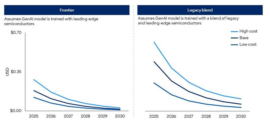
Source: Gartner (March 2026)
Falling Token Costs will not Democratize Frontier Intelligence
However, falling GenAI provider token costs will not be fully passed on to enterprise customers. Moreover, frontier intelligence will demand significantly more tokens than current mainstream applications. Agentic models, for example, require between 5-30 times more tokens per task than a standard GenAI chatbot, and can perform many more tasks than a human using GenAI.
While lower token unit costs will enable more advanced GenAI capabilities, these advancements will drive disproportionately higher token demand. As token consumption rises faster than token costs fall, overall inference costs are expected to increase.
“Chief Product Officers (CPOs) should not confuse the deflation of commodity tokens with the democratisation of frontier reasoning,” said Sommer. “As commoditised intelligence trends toward near-zero cost, the compute and systems needed to support advanced reasoning remain scarce. CPOs who mask architectural inefficiencies with cheap tokens today will find agentic scale elusive tomorrow.”
Value will accrue to platforms that can orchestrate workloads across a diverse portfolio of models. Routine, high-frequency tasks must be routed to more efficient small and domain-specific language models, which perform better than generic solutions at a fraction of the cost when aligned to specialised workflows. Expensive inference of frontier-level models must be heavily gated and reserved exclusively for high-margin, complex reasoning tasks.
The post Gartner Predicts That by 2030, Performing Inference on an LLM With 1 Trillion Parameters Will Cost GenAI Providers Over 90% Less Than in 2025 appeared first on ELE Times.
Infineon partners with Zenergize on power electronics for India’s energy transition
Київський політехнік Ігор Ментюков на Всесвітніх іграх майстрів

Київський політехнік Ігор Ментюков виступив у складі української футбольної команди ветеранів, яка виборола першість на Всесвітніх іграх майстрів. Нещодавно в місті Абу-Дабі (ОАЕ) відбулися Всесвітні ігри майстрів – ветеранів спорту.
Chiplets: 8 best practices for engineering multi-die designs

Semiconductor design is in the midst of a structural shift. For decades, performance gains were achieved by packing more transistors into single, monolithic dies. But the physical limitations of these dies—and the process technologies used to create them—are at odds with the ever-increasing compute, memory, and I/O demands of modern workloads. In other words, process technology advances alone are not enough to keep up with modern workloads.
Stepping in to address these demands are multi-die designs, which combine several smaller dies (known as chiplets) inside a single standard or advanced package. These multi-die architectures are reshaping how engineers build everything from AI accelerators to automotive ADAS systems. By disaggregating compute, memory, and I/O, teams can mix and match chiplets—often from different process nodes—to optimize performance, energy efficiency, size, or cost.
However, multi-die designs introduce new engineering complexities and design considerations, spanning packaging, verification, thermal dynamics, and more.
Here are eight best practices for developing chiplet designs.
- Leverage the ecosystem
Chiplet design is evolving through collaboration. Standards bodies such as the UCIe Consortium and JEDEC are defining interoperability, test, and reliability specifications. Research organizations like imec and ASRA are shaping automotive-grade chiplet guidelines. Leveraging this ecosystem reduces integration risk and helps ensure long-term compatibility.
Partnering with experienced IP and packaging vendors is also recommended. These providers can help teams fill resource and expertise gaps, focus on meaningful differentiation, and accelerate time to market.
- Partition with purpose
Every successful chiplet design for multi-die systems begins with smart partitioning. This means dividing the system into functional domains—such as compute, memory, and I/O—and determining the best process technology for each. Advanced nodes typically provide the highest performance and density, while mature nodes can often be used for less demanding functions to help reduce cost.
Establishing a partitioning strategy early in the design process helps prevent late-stage trade-offs and simplifies future upgrades. And using standards-based interfaces between chiplets keeps the architecture scalable, allowing future upgrades (using newer chiplets) without major redesign.
- Match node to function
The newest process node isn’t always the right one. Memory may not benefit from extreme scaling the way logic does, and analog or mixed-signal blocks often perform better on proven geometries. Selecting process nodes strategically—based on power, area, and yield targets—balances performance with manufacturability.
Design topology should also be considered. In 3D stacking, compute functionality based on the most advanced process nodes is typically placed on the top die, while I/O and SRAM functionality based on older, more cost-effective process nodes are placed on the bottom die. This approach lowers interconnect latency and power consumption but increases thermal complexity. Conversely, a 2.5D design—where chiplets are placed side-by-side—simplifies cooling and routing but often results in higher interconnect latency and power consumption.
- Treat packaging as part of the design
The package is no longer a container—it’s part of the circuit—and teams must choose from several options. Organic substrates, silicon interposers, and full 3D stacks offer varying levels of signal density, cost, and yield. As such, they should be evaluated alongside system architecture in the earliest phases of design exploration.
Testing and yield must also be considered. Each chiplet should be thoroughly validated as a known good die (KGD) prior to integration to ensure reliability. Incorporating hierarchical test features within each chiplet enables effective post-packaging verification.
Additionally, designing die-to-die interfaces with built-in redundancy and repair capabilities can help recover yield during assembly and address potential link failures throughout the product’s lifecycle. Because packaging materials and lead times vary among suppliers, early and proactive coordination with the supply chain is key to avoiding unexpected delays and ensuring a smooth production process.
- Engineer the interconnect like a subsystem
In multi-die designs, the communication between dies often defines overall performance. Die-to-die connectivity, bandwidth, latency, and signal integrity should be planned long before layout.
While standards such as UCIe are emerging to guide interoperability, each implementation faces unique physical challenges—including optimizing the “beachfront” area for micro bump placement, ensuring precise clock alignment, and managing routing density constraints.
- Verify the entire system
Traditional block-level verification is insufficient for multi-die designs. Integration across process nodes, tool flows, and packaging layers demands system-level verification from the outset. Multi-physics analysis should be performed on the die and complete multi-die system in a package.
Hardware-assisted verification, emulation, and fast simulation environments can reveal timing or interoperability issues that static tests miss. Hierarchical testing validates individual dies, then re-verifies the assembled system to confirm consistent performance. Adding thermal and crosstalk analysis closes the loop between electrical and mechanical design domains.
- Secure every interface
Multiple dies mean multiple entry points. Each chiplet must authenticate itself to the system and protect its data links. Embedding a root of trust (RoT) in a main or system chiplet can enable secure key management and firmware validation.
Encrypting traffic between chiplets prevents tampering, while a secure boot sequence ensures the system initializes only trusted code. Designing these controls at the architecture stage is far more effective than stitching them in later.
- Design for control and reliability
Complex packages benefit from a dedicated control and management subsystem, a small processor that handles initialization, telemetry, and security functions. This control layer also manages reliability, availability, and serviceability (RAS), gathering data from sensors across chiplets to detect issues before they escalate.
Telemetry from this subsystem helps engineers tune performance and maintain uptime, especially in data center and automotive environments where predictability is everything.
From integration to innovation
As the semiconductor industry transitions from monolithic dies to multi-die architectures, engineering teams must adopt new strategies to address the unique challenges and opportunities of chiplet-based designs. By leveraging industry ecosystems, partitioning systems purposefully, matching nodes to functions, treating packaging as integral to the design, engineering robust interconnects, verifying at the system level, securing every interface, and implementing dedicated control and reliability measures, organizations can maximize the benefits of chiplets—achieving enhanced performance, flexibility, and scalability.
Embracing these best practices will not only accelerate innovation but also ensure that multi-die solutions meet the demands of tomorrow’s complex applications.
Rob Kruger is product management director for multi-die strategy at Interface IP Product Management Group of Synopsys.
Special Section: Chiplets Design
- What the special section on chiplets design has to offer
- Chiplet innovation isn’t waiting for perfect standards
- Scoping out the chiplet-based design flow
- Demystifying 3D ICs: A practical framework for heterogeneous integration
The post Chiplets: 8 best practices for engineering multi-die designs appeared first on EDN.
Keysight Launches Local Manufacturing in India to Accelerate Global Innovation
Keysight Technologies has announced plans to begin local manufacturing in India, expanding its global production footprint to provide locally manufactured solutions for the country’s mission-critical industries. This strategic expansion enables Keysight to better serve its long-standing customer base—including aerospace and defence, government R&D, industry and academic research institutions—by providing streamlined procurement of world-class technology.
As India emerges as one of the world’s fastest-growing innovation economies, demand for advanced test and measurement technologies is increasing across all industrial and research sectors. India’s electronics manufacturing sector is expected to exceed $300 billion by 2026, driven by a surge in domestic production and advanced research initiatives.
The phased rollout of the new facility will focus on test equipment, serving both Indian and global customers while enhancing supply chain resilience. The move reinforces Keysight’s long-term commitment to India and aligns with the country’s flagship initiatives, including Make in India, Semicon India, the National Quantum Mission, as well as aerospace and defence modernisation programs.
“India is entering a once-in-a-generation innovation decade,” said Sudhir Tangri, Vice President and General Manager, Asia Pacific at Keysight. “Establishing local manufacturing allows Keysight to better support customers in India while strengthening our global supply chain. Building in India for the world will accelerate technology development across a broad spectrum of industries.”
Keysight’s manufacturing operations in India will support innovation across key sectors:
- Semiconductors: Enabling design validation and production testing as India expands its semiconductor industry under the Semicon India program.
- Quantum Technologies: Supporting research institutions and national laboratories advancing quantum computing under the National Quantum Mission.
- Aerospace and Defence: Providing advanced, locally manufactured test solutions for radar, electronic warfare, and satellite systems supporting India’s defence modernisation.
- Next-Generation AI and Wireless: Accelerating development and deployment of 5G and future 6G infrastructure, AI infrastructure and data centres.
- Research and Academia: Equipping universities and national laboratories with world-class tools for advanced engineering research and scientific discovery.
Keysight will continue to collaborate with Indian government agencies, research laboratories, and leading engineering universities to accelerate technology development and strengthen the country’s innovation ecosystem. The expansion reflects Keysight’s long-term strategy to invest in high-growth technology hubs that support customers developing the next generation of computing, communications, and national security systems.
The post Keysight Launches Local Manufacturing in India to Accelerate Global Innovation appeared first on ELE Times.
TAP Game - My DIY Reaction Game
 | This is TAP Game — my fully homemade pocket-sized two-player reaction game. How to play: Central SIGNAL LED blinks 3 times — get ready! After a random delay the signal lights up First player to smash their big tactile button wins the round Each player has 3 heart LEDs for score tracking First to 3 points wins the match Built-in anti-cheat / spam protection It runs on a single CR2032 coin cell using a bare ATmega328P (internal 8 MHz). Fully custom KiCad PCB, hand-soldered SMD components. Super compact and makes an excellent keychain for your keys! [link] [comments] |
Microchip Introduces Automotive-Qualified System-in-Package Hybrid MCU for Automotive and E-Mobility Human-Machine Interface Applications
 processor and 512 Mbit DDR2 SDRAM. The SAM9X75D5M supports large display sizes up to 10 inches and XGA resolution of 1024 × 768 pixels.
The post Microchip Introduces Automotive-Qualified System-in-Package Hybrid MCU for Automotive and E-Mobility Human-Machine Interface Applications appeared first on ELE Times.
Cadence and NVIDIA Collaborate on Accelerated Engineering Solutions for Agentic AI Chip and System Design
Cadence announced an expansion of its broad collaboration with NVIDIA to accelerate Cadence’s Design for AI and AI for Design strategy. The next generation of agentic AI design solutions includes autonomous, long-running agents that require accelerated, trusted, physics-grounded engines to translate design intent into automated flows, generate designs and debug errors, and manage long, complex, end-to-end workflows. Cadence’s leadership in agentic AI is expanded by integrating its portfolio of industry-leading chip and system design solutions with NVIDIA’s accelerated computing stack.
“The fusion of agentic AI and physics-based design is transforming how the world’s most advanced chips are engineered,” said Anirudh Devgan, president and CEO of Cadence. “Through our expanded collaboration with NVIDIA, we’re bringing together Cadence’s expertise in agentic IC design and physics-driven optimisation with NVIDIA’s accelerated computing to advance a new era of AI-driven chip innovation. Together, we’re enabling customers to design more intelligent, efficient silicon that will power the next generation of computing and AI infrastructure.”
“AI is driving the largest infrastructure buildout in history—spurring the creation of new chips, systems, and AI factories around the world,” said Jensen Huang, founder and CEO of NVIDIA. “Together, NVIDIA and Cadence have created the Cadence Millennium M2000—a revolutionary AI supercomputer built to tackle the immense scale and complexity of designing the world’s next generation of infrastructure.”
Broadest-Ever Portfolio of Accelerated Design Solutions
To give agents and engineers the tools they need, Cadence has expanded its design solutions accelerated with NVIDIA Grace CPUs and NVIDIA Blackwell GPUs—and as a turnkey deployment on the Cadence Millennium M2000 Supercomputer—delivering up to 80X greater throughput and up to 20X lower power consumption. This expanded offering now spans analysis, optimisation, and design, with key solvers deeply optimised with NVIDIA CUDA-X. One example is the Cadence Clarity 3D Solver demonstrating that a Millennium M2000 system configured with 8X NVIDIA RTX Pro 6000 GPU servers is up to 5X faster, or 4X better cost iso-performance, compared to an equivalent CPU-based solution, when extracting complex and large-scale designs.
Cadence accelerated solutions that will be available in 2026 include:
- Electronic Design Automation (EDA): The industry’s leading place-and-route solution, Innovus Implementation System; chip, chiplet and 3D-IC analysis and optimisation with Celsius Thermal Solver and Voltus IC Power Integrity Solution; advanced memory and circuit analysis with EMX Planar 3D Solver and Liberate MX Memory Characterisation; and Spectre X Simulator and Quantus Field Solver for circuit analysis.
- System Design Automation (SDA): Industry-leading advanced package and PCB optimisation with the Allegro X Design Platform, Clarity 3D Solver, Celsius EC Solver; system-level multiphysics analysis with Fidelity CFD Software; and Cadence MSC Actran for physical AI system analysis and optimisation.
- Life Sciences / Bio: ROCS X is an AI-enabled virtual screening solution that enables scientists to conduct 3D searches of over 200 trillion drug-like molecules. Target X is a physics-based AI solution that detects potential druggable pockets, achieving a success rate of over 90%.
The Cadence Allegro X Design Platform and the Cadence Reality Digital Twin Platform also integrate with NVIDIA Omniverse libraries for photo-realistic visualisation, critical for multi-disciplinary engineering and design. Cadence’s MSC Virtual Test Drive (VTD) is being integrated with NVIDIA Cosmos and NVIDIA Omniverse NuRec for advancing the state of the art in physical AI.
Design for AI and AI for Design
Industry leaders use Cadence’s full suite of accelerated agentic solutions to design the next generation of AI infrastructure. The Cadence Reality Digital Twin Platform helps teams use physics-based models and AI to design and operate AI factories, accelerating deployment timelines and unlocking new revenue streams across the data centre portfolio.
Cadence is advancing AI-driven engineering with its agentic AI solutions, led by the Cadence ChipStack AI Super Agent, to help engineers deliver higher quality, more complex designs. Cadence and NVIDIA are also collaborating on future agentic AI innovations in custom and analogue design and building deep research and long-running agents for engineering NVIDIA NemoClaw, an open source stack that simplifies running OpenClaw always-on assistants, more safely, with a single command. As part of the NVIDIA Agent Toolkit, it installs the NVIDIA OpenShell runtime—a secure environment for running autonomous agents, and open source models like NVIDIA Nemotron.
From Silicon to Turbofan Engines, Customers Achieve the Previously Impossible
Cadence customers across semiconductors, automotive, aerospace and life sciences are using agentic AI, GPU-accelerated solutions and the Millennium M2000 Supercomputer to tackle design challenges that are not achievable with traditional approaches.
Honda is using Cadence Fidelity CFD Software, accelerated on the Millennium M2000 GB200 NVL72 system, to pursue time-accurate, full turbofan engine simulation—a grand challenge in computational fluid dynamics (CFD) previously impractical for routine design use.
“This capability opens the door to a more exploratory design methodology—one where our engineers can evaluate tradeoffs earlier and innovate with greater confidence as we develop the next generation of high-performance gas turbine engines,” said Keiji Otsu, CEO, Honda R&D.
Micron is integrating GPU-accelerated Cadence design technologies and Cadence’s agentic AI solution directly into its HBM memory design flow to accelerate iteration and maintain accuracy at leading-edge scale.
“As our HBM and next-generation memory designs grow in scale and complexity, reducing the cycle time for our most demanding verification and simulation steps has become essential,” said Sanjay Mehrotra, Chairman, president and CEO, Micron. “Through our expanded collaboration with Cadence, we’re integrating GPU-accelerated design technologies—powered by NVIDIA computing—and building agentic AI directly into our development environment.”
Larsen & Toubro Semiconductor is using the Cadence Spectre X Simulator, accelerated up to 5X with NVIDIA GPUs, to shorten design cycles for next-generation AI and data centre chips as the company advances India’s sovereign semiconductor ambitions.
“Faster design iteration and verification directly translate into competitive advantage and time to market for the highly customised AI silicon we’re building,” said Sandeep Kumar, CEO, Larsen & Toubro Semiconductor. “GPU-accelerated performance from Cadence’s Spectre X Simulator gives our teams the throughput to confidently move complex, AI-ready chips into production faster.“
The post Cadence and NVIDIA Collaborate on Accelerated Engineering Solutions for Agentic AI Chip and System Design appeared first on ELE Times.
TI unveils high-performance isolated power modules to advance power density in data centers and EVs
Texas Instruments (TI) has unveiled new isolated power modules, helping enable increased power density, efficiency and safety in applications ranging from data centres to electric vehicles (EVs). The UCC34141-Q1 and UCC33420 isolated power modules leverage TI’s IsoShield technology, a proprietary multichip packaging solution that achieves up to three times higher power density than discrete solutions in isolated power designs. TI is showcasing these innovations at the 2026 Applied Power Electronics Conference (APEC), March 23-26 in San Antonio, Texas.
“Packaging innovation is revolutionising the power industry, with power modules at the forefront of this transformation,” said Kannan Soundarapandian, vice president and general manager, High Voltage Products at TI. “TI’s new IsoShield technology delivers what power engineers need most: smaller solutions with improved efficiency and reliability, and a faster time to market. It is the latest example of TI’s continued commitment to advance power semiconductor technology to help solve today’s engineering challenges.”
Redefining power density with TI’s packaging technology
Historically, power designers have turned to power modules to conserve valuable board space and simplify the design process. As chip sizes reach their physical limits and miniaturisation increases in importance, advancements in packaging technology are enabling further performance and efficiency gains.
TI’s new IsoShield technology combines a high-performance planar transformer with an isolated power stage, offering functional, basic, and reinforced isolation capabilities. It enables a distributed power architecture, helping manufacturers meet functional safety requirements by avoiding single-point failures. The result is a packaging advancement that shrinks solution size by as much as 70% while delivering up to 2W of power, enabling compact, high-performance and reliable designs for automotive, industrial and data centre applications that require reinforced isolation.
Advancing data centre and EV performance through power innovations
Power density innovations are nowhere more critical than in today’s evolving data centre and automotive designs. Meeting design requirements in those applications starts with advanced analogue semiconductors – the components that enable smarter, more efficient operations. As global data centres continue to scale to meet exponentially growing demand, high-performance power modules must pack more power in smaller spaces. With TI’s IsoShield packaging technology, designers can achieve higher power density in compact form factors, ensuring reliable and safe operation of the world’s digital infrastructure. Similarly, the increased power density enabled by IsoShield technology helps engineers design lighter and more efficient EVs that significantly extend range and enhance performance.
Building on our power module innovation
For decades, TI has strategically invested in power management technology, with recent developments in power modules that feature integrated transformers and integrated inductors. Through innovative proprietary packaging solutions such as IsoShield and MagPack technologies, along with a comprehensive portfolio of over 350 power modules with optimised packages, TI’s semiconductors empower engineers to maximise performance in any power design or application.
Innovating what’s next in power at APEC 2026
In booth No. 1819 at the Henry B. González Convention Centre, TI will feature the isolated power modules with IsoShield technology in a high-power, high-performance automotive silicon carbide (SiC) 300kW traction inverter reference design. Additionally, TI will debut other advancements in data centers, automotive, humanoid robots, sustainable energy and USB Type-C® applications, including an 800V to 6V DC/DC power distribution board. This design features TI’s portfolio of gallium nitride integrated power stages, digital isolators and microcontrollers that help enable high efficiency and power density in power conversion for next-generation data center computing trays with AI processors.
The post TI unveils high-performance isolated power modules to advance power density in data centers and EVs appeared first on ELE Times.
STMicroelectronics Unveils AI-Enabled ‘Stellar P3E’ MCU, Backs 28nm Strategy for Cost and Supply Chain Stability
By Shreya Bansal, Sub-Editor
STMicroelectronics introduced the Stellar P3E, a next-generation automotive microcontroller with embedded artificial intelligence (AI) acceleration, positioning it as a key enabler for software-defined vehicles (SDVs) and consolidated “X-in-1” electric vehicle architectures.
Announced during a media briefing, the Stellar P3E marks a significant step in integrating real-time AI with deterministic control, addressing the rising complexity of modern automotive systems driven by electrification and connectivity.
Powering the X-in-1 Transition
Automakers are increasingly shifting toward “X-in-1” architectures, which consolidate multiple functions, such as battery management, onboard charging, and power conversion into a single system. This reduces hardware redundancy, wiring, and overall system weight.
The Stellar P3E is designed to sit at the centre of this transition, combining high-performance computing, advanced analogue integration, and AI capabilities in a single chip.
Embedded AI for Real-Time Intelligence
A key highlight of the new MCU is its Neural ART Accelerator, a dedicated neural processing unit (NPU) that enables real-time AI inference at the edge. The accelerator is capable of significantly reducing inference time, up to 69 times faster than CPU-based implementations, while maintaining low power consumption.
This allows vehicles to process unstructured data, detect patterns, and adapt system behaviour dynamically, supporting applications such as predictive maintenance, intelligent sensing, and optimised energy management.
Addressing Industry-Wide Complexity
With vehicles evolving into software-driven platforms, the industry is facing unprecedented challenges, including exponential software growth, stricter safety and cybersecurity requirements, and ongoing supply chain uncertainties.
STMicroelectronics emphasised three key pillars behind the Stellar P3E:
- Reducing complexity and cost through hardware consolidation and software optimisation
- Enabling smarter systems with AI-driven algorithms
- Delivering high-performance computing with precise sensing and actuation
The MCU also complies with ISO 21434 cybersecurity standards and incorporates flexible safety configurations, including split-lock and lockstep modes.
High Performance, Rich Integration
The Stellar P3E delivers up to 8,000 CoreMark performance and features:
- Up to 19.5 MB of embedded non-volatile memory using phase-change memory (PCM)
- Over 300 GPIOs and more than 100 ADC channels
- Support for Gigabit Ethernet and CAN-XL communication
These capabilities enable integration of multiple powertrain components, including inverters, DC-DC converters, and battery systems within a unified architecture.
Industry Shift to Software-Defined Vehicles
The launch aligns with the broader move toward software-defined vehicles, where functionality is increasingly delivered through software updates rather than hardware changes. With support for over-the-air (OTA) updates and scalable memory, the Stellar P3E enables continuous feature upgrades over a vehicle’s lifecycle.
The company is targeting a $16 billion automotive MCU market opportunity by 2030, driven by electrification, ADAS, and SDVs.
Why 28nm Still Matters: ST Explains Its Node Strategy
When asked about ST’s decision to use a 28-nanometer process node at a time when competitors are pushing toward more advanced nodes, they clarified that while advanced nodes are typically optimised for maximum compute efficiency, they are not always cost-effective for automotive applications that require a balance of digital processing and analogue functionality.
The company stated that 28nm represents a “sweet spot” where both analogue performance and digital complexity can be efficiently integrated. It also highlighted its advantage in embedding large memory at this node, leveraging what it described as one of the densest technologies in the industry.
On the supply chain front, ST emphasised its vertically integrated manufacturing strategy. The 28nm technology used for Stellar P3E is produced at its high-capacity facility in Crolles, France, allowing the company to retain greater control over production.
Unlike reliance on external foundries, which are currently under pressure from AI-driven demand, ST’s in-house manufacturing enables it to prioritise automotive and industrial customers. The company also noted its dual-sourcing strategy for automotive MCUs at every stage of production to enhance resilience.
The post STMicroelectronics Unveils AI-Enabled ‘Stellar P3E’ MCU, Backs 28nm Strategy for Cost and Supply Chain Stability appeared first on ELE Times.
Infineon and DG Matrix partner to drive solid-state transformer technology for AI data centers and industrial power applications
Voltage multiplier
 | I've been designing this 6-stage symmetrical half-wave voltage multiplier build. I was planning to build it like this: battery->zvs circuit for getting ac and proper 50kHz frequency->small transformer for upping the voltage to 10kV->multiplier. The lower part generates negative voltage, and the upper part positive, both 120kV so combined they give a 240kV spark. [link] [comments] |
Power Integrations extends flyback topology to 440W, offering simpler alternatives to resonant power designs
Power Integrations extends flyback topology to 440W, offering simpler alternatives to resonant power designs
Toshiba showcases power semiconductor solutions at APEC
Сторінки


![[link]](https://i.redd.it/5ualhpo0i1rg1.jpeg)