


Збирач потоків
Brain-Computer Interfaces (BCIs) & Neurotechnology: The Next Frontier in Electronics Engineering
The convergence of neuroscience, electronics, and artificial intelligence is driving one of the most transformative technological revolutions of the 21st century: Brain-Computer Interfaces (BCIs) and neurotechnology. Once confined to science fiction, BCIs are now rapidly evolving into practical systems capable of enabling direct communication between the human brain and external electronic devices. For electronics engineers, this emerging domain offers exciting opportunities in embedded systems, signal processing, flexible electronics, biomedical instrumentation, and AI-driven hardware development.
The Rise of Brain-Computer Interfaces
A Brain-Computer Interface is a system that acquires neural signals, processes them, and translates them into commands for computers, prosthetics, or other electronic systems. Traditional BCIs relied on electroencephalography (EEG), where electrodes placed on the scalp measure brainwave activity. While non-invasive EEG systems remain important for research and healthcare applications, recent advances in high-density electrode arrays and implantable bioelectronics are dramatically improving signal quality and functionality.
Modern BCIs can now interpret neural activity with remarkable precision, enabling paralyzed individuals to control robotic limbs, type text using thought alone, and even regain limited speech capabilities. The integration of machine learning algorithms with neural signal acquisition hardware has accelerated these developments significantly.
Flexible Bioelectronics: A Game Changer
One of the biggest engineering challenges in neurotechnology has been the mechanical mismatch between rigid electronic devices and soft biological tissues. Conventional silicon-based implants often trigger inflammation or degrade over time due to tissue damage. Flexible bioelectronics are solving this issue.
Flexible neural interfaces are built using biocompatible materials such as polyimide, graphene, conductive polymers, and ultra-thin gold traces. These devices can bend and stretch with brain tissue, reducing long-term damage and improving signal stability. Engineers are also exploring bioresorbable electronics that safely dissolve in the body after completing their function.
For electronics engineers, flexible electronics require innovation in several areas:
- Low-power integrated circuit design
- Stretchable conductive materials
- Miniaturized sensor architectures
- Wireless power transfer systems
- High-speed neural signal amplification
These systems must operate reliably while consuming extremely low power to minimize heat generation near sensitive neural tissue.
High-Density Electrode Arrays and Neural Mapping
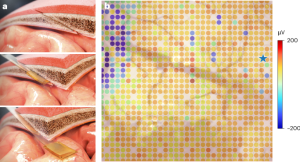
High-density electrode arrays are enabling researchers to record thousands of neurons simultaneously. Companies and research institutions are developing microelectrode arrays with unprecedented spatial resolution, allowing detailed mapping of neural activity patterns.
Advanced semiconductor fabrication techniques are making it possible to integrate thousands of microscopic electrodes onto a single chip. These arrays are combined with custom ASICs (Application-Specific Integrated Circuits) for signal amplification, filtering, analog-to-digital conversion, and wireless communication.
The data bandwidth generated by these systems is enormous. A next-generation BCI may process gigabits of neural data every second, creating major opportunities for engineers specializing in:
- Edge AI processing
- FPGA-based neural computing
- Real-time DSP systems
- Wireless telemetry
- Neuromorphic processors
Neuromorphic engineering, inspired by the architecture of the human brain, is becoming particularly important for efficient neural data processing. Unlike conventional processors, neuromorphic chips mimic biological neural networks and consume significantly less power.
Applications Transforming Healthcare
Healthcare remains the most promising application area for BCIs and neurotechnology. Neuroprosthetics are helping amputees control robotic limbs using brain signals with increasing accuracy and natural movement. Cochlear implants and retinal prostheses are restoring sensory functions to patients with hearing and vision impairments.
In neurological diagnostics, implantable neural sensors can monitor epilepsy, Parkinson’s disease, and other disorders in real time. Closed-loop neurostimulation systems can detect abnormal brain activity and automatically deliver corrective electrical stimulation.
Researchers are also investigating memory enhancement, depression treatment, and cognitive rehabilitation through targeted neural stimulation. These advancements depend heavily on reliable biomedical electronics and ultra-low-noise analog front-end design.

Patient controlling robotic prosthetic arm using BCI technology
Challenges and Ethical Considerations
Despite rapid progress, significant challenges remain. Neural signals are extremely weak and susceptible to noise, requiring sophisticated filtering and signal conditioning techniques. Long-term implant reliability, cybersecurity, and wireless communication safety are also major concerns.
Ethical issues surrounding cognitive enhancement, neural privacy, and brain data ownership are becoming increasingly important. As BCIs evolve from medical devices to consumer technologies, electronics engineers will play a critical role in designing secure and responsible systems.
Power management is another key challenge. Implantable devices require efficient energy harvesting or wireless charging technologies to avoid repeated surgical battery replacement. Advances in ultra-low-power electronics and energy-efficient communication protocols will be essential.
The Future of Neurotechnology
The future of BCIs lies in seamless human-machine integration. Emerging systems may eventually enable direct brain-to-brain communication, immersive virtual reality control, and advanced cognitive augmentation. Artificial intelligence combined with adaptive neural interfaces could create highly personalized neuroprosthetic systems capable of learning and evolving with users.
For electronics engineers, neurotechnology represents a multidisciplinary field where expertise in electronics, embedded systems, materials science, AI, and biomedical engineering converge. As the boundaries between biology and electronics continue to blur, BCIs are poised to become one of the defining technologies of the coming decades.
The era of intelligent bioelectronic systems has begun — and electronics engineers are at the center of this technological transformation.
The post Brain-Computer Interfaces (BCIs) & Neurotechnology: The Next Frontier in Electronics Engineering appeared first on ELE Times.
Brain-Inspired Neuromorphic Computing: Moving Beyond Traditional Processor Architectures
For more than five decades, the computing industry has relied on the von Neumann architecture, where memory and processing units are physically separated. While this architecture has enabled remarkable advances in computing power, it also faces significant challenges in today’s data-driven world. The continuous movement of data between memory and processors consumes enormous amounts of energy and creates performance bottlenecks, particularly in artificial intelligence (AI) and edge computing applications.
To address these limitations, researchers and semiconductor companies are increasingly turning to a radically different approach inspired by nature’s most efficient computing system—the human brain. Neuromorphic computing represents a paradigm shift in processor design, enabling machines to process information more like biological neural networks while consuming a fraction of the energy required by conventional systems.
Understanding Neuromorphic Computing
Neuromorphic computing refers to the design of hardware systems that mimic the structure and operation of the human brain. Unlike traditional processors that execute instructions sequentially, neuromorphic chips consist of artificial neurons and synapses that operate in parallel and communicate through event-driven signals known as spikes.
The human brain contains approximately 86 billion neurons interconnected through trillions of synapses. Despite this immense complexity, the brain operates on roughly 20 watts of power—less than many household light bulbs. Neuromorphic engineers aim to replicate this extraordinary efficiency in silicon.
In a neuromorphic system:
- Artificial neurons process incoming signals.
- Synapses store connection strengths and learning parameters.
- Information is transmitted only when meaningful events occur.
- Memory and computation are closely integrated.
- Learning can occur directly on the device.
This architecture significantly reduces the energy and latency associated with moving data between separate memory and processing units.
Why Traditional Architectures Are Reaching Their Limits
Modern AI applications generate enormous volumes of data from sensors, cameras, microphones, and connected devices. Conventional CPUs and GPUs must continuously shuttle this data between memory and processing cores, creating what is commonly known as the “memory wall.”
Key limitations include: High Power Consumption, Latency Challenges and Scalability Constraints. Neuromorphic computing addresses these challenges by bringing memory, learning, and processing closer together in a brain-like architecture.
Event-Driven Processing: The Key to Efficiency
One of the most innovative aspects of neuromorphic systems is event-driven computation. Traditional processors operate continuously, executing clock cycles whether useful work is being performed or not. Neuromorphic chips, however, remain largely inactive until significant events occur.
For example, consider a surveillance camera monitoring a quiet corridor. A conventional AI processor continuously analyzes every video frame. A neuromorphic processor only activates when movement or a meaningful change is detected. The result is intelligent systems that can remain operational for extended periods without frequent charging or cloud connectivity.
Real-Time Learning at the Edge
One of the most promising capabilities of neuromorphic hardware is on-device learning. Traditional AI systems are typically trained in data centers and deployed as fixed models. Updating these models often requires cloud access, large datasets, and significant computational resources.
Neuromorphic chips can adapt continuously based on experience, much like biological brains. This capability enables: Personalized Wearables, Autonomous Robots, Smart Sensors and Adaptive Industrial Systems. Such capabilities are particularly valuable in environments where network connectivity is limited or unavailable.
Applications Across Industries: Autonomous Vehicles: Self-driving vehicles process enormous amounts of sensory information from cameras, radar, LiDAR, and ultrasonic sensors. Healthcare and Wearables: Smart medical devices require continuous monitoring while maintaining long battery life. Industrial Automation: Factories increasingly rely on intelligent edge devices for predictive maintenance, quality inspection, and process optimization. Aerospace and Defense: Autonomous drones and surveillance systems benefit from low-power AI processing capable of operating independently in challenging environments. Internet of Things (IoT): Billions of connected devices generate vast quantities of sensor data.
Leading Neuromorphic Hardware Developments
Several organizations are actively advancing neuromorphic technology: Intel Corporation has developed the Loihi family of neuromorphic research chips capable of on-chip learning and adaptive processing. IBM pioneered large-scale neuromorphic architectures with its TrueNorth processor. European Human Brain Project has invested heavily in brain-inspired computing research. Numerous startups are developing specialized neuromorphic solutions for edge AI, robotics, and industrial applications.
Technical Challenges Ahead
Despite significant progress, neuromorphic computing remains an emerging field. Key challenges include: Programming Complexity: Developing software for spiking neural networks differs substantially from conventional programming methodologies. Ecosystem Maturity: Tools, frameworks, and standards remain less mature than those available for CPUs, GPUs, and traditional AI accelerators. Commercial Scalability: Manufacturing and integrating neuromorphic hardware into mainstream products requires further technological advancement and industry adoption. Benchmarking Difficulties: Comparing neuromorphic performance against conventional systems remains challenging because the architectures operate fundamentally differently.
The Future of Brain-Inspired Computing
As AI increasingly moves from centralized data centers to intelligent edge devices, energy efficiency and real-time adaptability become critical requirements. Neuromorphic computing offers a compelling solution by emulating the principles that make the human brain remarkably powerful and efficient.
Rather than replacing traditional CPUs and GPUs entirely, neuromorphic processors are likely to emerge as specialized accelerators for applications requiring low power consumption, continuous learning, and rapid decision-making at the edge.
For working engineers, neuromorphic computing represents more than just another processor innovation. It signals the beginning of a new computing paradigm where machines learn, adapt, and respond with unprecedented efficiency. As edge AI, robotics, autonomous systems, and wearable technologies continue to expand, brain-inspired architectures may become a foundational component of next-generation intelligent systems.
Neuromorphic computing is redefining how engineers think about processing, memory, and intelligence. By mimicking the brain’s structure and operation, neuromorphic chips achieve remarkable energy efficiency while enabling real-time learning and adaptation.
The post Brain-Inspired Neuromorphic Computing: Moving Beyond Traditional Processor Architectures appeared first on ELE Times.
AI-Augmented Test Automation: Transforming Enterprise-Scale System Validation
Enterprise software is no longer built for stability. It is built for continuous change. Modern systems evolve over distributed architectures, cloud-native platforms, and microservice ecosystems, with release cycles measured in days rather than months. Against this rapid evolution, the customary boundaries of testing are being fundamentally redefined.
Validation, once a discrete phase in the development lifecycle, now operates under constant pressure to keep pace with rapid deployment. The challenge is no longer simply guaranteeing correctness, but doing so continuously, at scale, and amid mounting system complexity.
Conventional automation frameworks, designed for predictability and control, are beginning to show their limitations. As systems evolve dynamically, static test scripts and rule-based execution models struggle to remain effective. It is within this context that AI-augmented test automation is emerging not as a replacement, but as an essential evolution of how enterprise systems are validated.
From Scripted Automation to Adaptive Testing SystemsTraditional automation has long relied on predefined scripts and deterministic workflows. While this strategy delivers consistency, it is inherently rigid. Even minor changes in application interfaces or workflows is able to disrupt test execution, causing frequent maintenance cycles that consume time and engineering effort.
AI introduces adaptability into this equation, fundamentally shifting the testing landscape. By using historical data, execution patterns, and system behaviour, AI-augmented frameworks can interpret changes and operate dynamically. As a result, testing systems begin to move past static execution toward context-aware validation, where decisions are informed by data rather than predefined rules alone.
This shift isn’t incremental; it is a redefinition of automation itself. Testing no longer centres solely on executing what is known, but on intelligently responding to what changes. As Satya Nadella has emphasised, “Every company is becoming a software company, and agility is key regarding innovation.” In such an environment, testing must evolve into an enabler of that agility, not a constraint on it.
The Scaling Challenge: Complexity at Enterprise LevelAt enterprise scale, testing is not simply about validating features—it is about ensuring the coordinated functioning of distributed systems. Applications span multiple services, environments, and configurations, each introducing its own layer of variability.
What makes this challenge particularly significant is not just the volume of test cases, but the rate at which they become outdated. As systems change, test suites expand, execution times increase, and maintenance overhead grows disproportionately.
The core pressures can be summarized as:
- Expanding and continuously evolving test suites
- Increasing difficulty in maintaining reliable test execution
- The need for comprehensive coverage across diverse system states
These challenges do not scale linearly—they compound. Without intelligent optimization, testing becomes a bottleneck, slowing down the very innovation it is meant to support. AI-augmented automation addresses this by introducing prioritization, reducing redundancy, and aligning testing efforts with actual system risk.
Resilience Through Self-Healing AutomationOne of the most tangible advancements enabled by AI is the concept of self-healing automation. In traditional systems, test failures often result from minor interface changes—renamed elements, altered layouts, or modified identifiers. These failures require manual intervention, creating inefficiencies in otherwise automated workflows.
AI-driven systems mitigate this limitation by recognizing patterns and relationships within application structures. Instead of failing immediately, they can identify alternative elements or pathways, allowing tests to continue execution. This capability significantly reduces maintenance cycles and enhances overall system resilience.
More importantly, it shifts the role of automation from a fragile executor to a robust validation layer capable of adapting alongside the applications it tests.
Intelligent Test Design: From Coverage to Risk-Based ValidationA critical evolution in AI-augmented testing also lies in how test cases are generated and optimised. Established approaches often prioritise exhaustive coverage, leading to large but inefficient test suites. In contrast, AI enables a more strategic model—one that focuses on risk, impact, and system operation.
More specifically, by analysing historical defects, usage patterns, and code changes, AI systems can identify which areas of an application are most likely to fail and prioritise testing accordingly. This switch from coverage-driven to risk-based validation amounts to a significant improvement in both capability and effectiveness.
Instead of attempting to execute all possible scenarios, testing becomes targeted and adaptive, ensuring that critical paths receive the highest level of scrutiny, thus increasing the effectiveness of the entire process.
Continuous Testing in High-Velocity PipelinesIntegrating testing into CI/CD pipelines has fundamentally changed how software is delivered. While the speed of these pipelines is transformative, it also introduces challenges. Testing must provide rapid, reliable feedback without becoming a performance bottleneck.
AI addresses this by introducing decision intelligence into test execution. Rather than running all tests indiscriminately, systems select and prioritise tests based on relevance to recent changes. This reduces execution time while maintaining validation quality.
In this model, testing is no longer a passive checkpoint; it becomes an active, intelligent participant in the delivery pipeline, continuously adjusting to the system’s evolving state.
From Test Execution to Quality Intelligence
Looking beyond automation and execution, AI delivers a wider transformation: the evolution of testing into a source of engineering intelligence. By analysing large volumes of test data, system logs, and defect histories, AI systems can discover patterns that inform not only testing strategies but also system design decisions.
This shift repositions testing from a reactive activity to an anticipatory capability. Instead of identifying defects after they occur, systems can predict possible failure points and guide engineering efforts toward more robust designs.
In this sense, testing acts not only as a validation function but also as a contributor to overall system quality and reliability.
Human Expertise in an AI-Augmented EcosystemDespite the growing role of AI, human expertise remains central to the testing process. AI excels at handling scale, pattern recognition, and repetitive execution, but it lacks contextual judgment and domain-specific insight.
Human testers bring critical thinking, scenario understanding, and strategic supervision capabilities that cannot be fully automated. The most effective testing environments are therefore not AI-driven in isolation, but AI-augmented, where people and computers’ capabilities complement each other.
This balance ensures that, as efficiency improves, the depth and reliability of validation are not compromised.
Adoption Realities: Engineering and Integration ChallengesThe adoption of AI-augmented testing is not free from challenges. Integrating intelligent systems into existing enterprise environments requires careful planning, particularly in data quality, tool compatibility, and workflow alignment.
Organisations must ensure sufficient data is available to train AI models effectively, while also preserving transparency in decision-making. Integration with legacy systems can make deployments more complex, requiring incremental adoption strategies.
These considerations highlight an important reality: the transition to AI-augmented testing is as much an organisational shift as it is a technological one.
Future Outlook: Toward Autonomous Testing EcosystemsGoing forward, the trajectory of test automation points toward increasing autonomy. AI systems are expected to take on more responsibility in managing test lifecycles, from generation and execution to optimisation and maintenance.
Future systems will not only execute tests but also constantly learn from outcomes, improving strategies and adjusting to evolving system behaviour. This progression moves testing closer to a self-sustaining ecosystem, where validation progresses alongside the software it supports.
As Sundar Pichai has noted, “AI is one of the most profound technologies we are working on.” Its application in testing demonstrates a broader transformation, one in which intelligence becomes embedded in the core of engineering processes.
Conclusion: Redefining the Role of Testing in Enterprise SystemsAI-augmented test automation represents more than an enhancement of existing practices; it constitutes a fundamental change in how enterprise systems are validated. In an age distinguished by speed, scale, and complexity, established approaches are no longer sufficient.
Testing must evolve into an intelligent, adaptive capability, one that not only verifies system operation but also actively contributes to its reliability and dependability. AI enables this transformation by introducing adaptability, insight, and capability into every stage of the testing lifecycle.
As enterprise systems continue to grow in complexity, the role of AI in testing will become increasingly central. The future of quality assurance will not be defined by how extensively systems are tested, but by how intelligently they are validated consistently, efficiently, and at scale.
The post AI-Augmented Test Automation: Transforming Enterprise-Scale System Validation appeared first on ELE Times.
MLPerf and the rise of latency-aware LLM benchmarking

Any discussion of modern AI system performance must include MLCommons and its MLPerf benchmark suite, which has become the industry’s de facto standard for measuring machine learning performance. Since its debut in 2018, MLPerf has provided a neutral, peer-reviewed framework for comparing hardware and software platforms across a broad range of AI workloads.
The original MLPerf benchmarks reflected the dominant AI workloads of the late 2010s. Early inference tests focused on models such as image classification with ResNet-50, natural language processing with Bidirectional Encoder Representations from Transformers (BERT), object detection with RetinaNet, and recommendation with Deep Learning Recommendation Model (DLRM).
These workloads were important and representative at the time, but they shared one characteristic: they were highly parallel and relatively easy to map onto GPU architectures.
For several years, benchmark results reinforced a simple narrative. Each new generation of accelerators delivered higher throughput, lower latency, and better energy efficiency. Because the workloads aligned well with GPU strengths, the benchmark curves rose steadily and predictably.
The generative AI shockwave: Rewriting the rules of MLPerf
Autoregressive LLMs introduced a fundamentally different inference pattern. Prompt processing remained highly parallel, but token generation became sequential and memory bound. Suddenly, raw TeraFLOPS no longer told the whole story.
MLPerf began incorporating this new reality in stages. Inference v4.0 introduced the first LLM benchmark based on Meta platform Llama 2 70B. This benchmark measured token throughput and provided the industry with its first standardized method for comparing LLM inference systems.
MLPerf Inference v5.0 released in 2025 significantly expanded the generative AI focus. It added Llama 3.1 405B Instruct, a 405-billion parameter model with a 128,000-token context window. The benchmark also introduced an interactive variant of Llama 2 70B that imposed strict limits on Time to First Token (TTFT) and Time Per Output Token (TPOT), two metrics that directly capture user experience in conversational applications.
These additions were pivotal because they exposed the core weakness of GPU-based inference systems. When unconstrained by latency, GPUs could buffer requests, create large batches, and deliver excellent throughput. Under interactive latency limits, batching opportunities shrank, hardware utilization dropped, and throughput fell sharply.
In other words, MLPerf began measuring not just how fast a system could run under ideal conditions, but also how responsive it remained under realistic conditions.
Inference disaggregation: Optimization of resources
This evolution reached another milestone in MLPerf Inference v5.1 and the emerging v6.x era. The benchmark suite broadened its focus to include increasingly sophisticated workloads, including reasoning models such as DeepSeek-R1 and more demanding long-context applications. At the same time, submissions began showcasing system-level optimizations such as inference disaggregation, where prompt processing and decoding are assigned to different accelerator pools.
Disaggregation has become one of the most consequential developments in modern inference benchmarking.
Historically, MLPerf treated each benchmark run as a single system under test, leaving vendors free to optimize their hardware and software stacks as they saw fit. As long as submissions complied with accuracy and latency requirements, any architectural technique was fair game.
This openness allowed participants to introduce increasingly sophisticated serving strategies. One of the most effective has been the separation of prefill and generation across distinct groups of accelerators. The prefill cluster handles the compute-intensive prompt processing stage, while the generation cluster focuses exclusively on token decoding.
In controlled benchmark scenarios, where prompt lengths and output lengths are known in advance, disaggregation can produce dramatic gains. By eliminating interference between the two phases, systems reduce preemption and improve latency-sensitive throughput.
Yet this raises an important question. Does the benchmark still measure accelerator capability, or is it increasingly measuring system orchestration? The answer is both.
Modern AI performance depends on the interaction between processor, memory hierarchy, interconnect fabric, runtime software, and serving algorithms. MLPerf has evolved accordingly. It now rewards system-level innovation rather than isolated chip performance.
That shift is entirely appropriate, but it also means benchmark results must be interpreted carefully.
A disaggregated configuration optimized for long document summarization may perform brilliantly in MLPerf while delivering more modest benefits in production environments where workloads vary continuously. Real-world deployments must cope with unpredictable prompt lengths, bursty traffic, and rapidly changing ratios of prefill to generation demand.
Consequently, MLPerf increasingly measures a system’s ability to align resources with a known workload profile. This is a valuable metric, but it’s not synonymous with universal real-world performance.
Illustrative comparison: MLPerf 5.x versus MLPerf 6.x
Table below illustrates how benchmark methodology evolved as MLPerf shifted from throughput-oriented LLM tests to more latency-sensitive and system-aware workloads. The numbers are representative rather than exact, but they reflect the broad trends seen in published results and vendor disclosures.

Publicly discussed MLPerf inference results based on Llama 3.1 405B LLM run on a leading-edge GPU-based processor in three scenarios (off-line, server mode, and interactive mode) highlight MLPerf’s evolution. Source: Author
From chip benchmark to system benchmark
The history of MLPerf mirrors the evolution of AI itself.
The early benchmark suites focused on relatively static workloads that aligned naturally with the strengths of GPU architectures. Tasks such as image recognition, recommendation systems, and conventional deep learning inference relied heavily on dense matrix operations and large-scale parallelism, allowing GPUs to demonstrate exceptional throughput and scalability. In that era, benchmark leadership was closely associated with raw compute capability, memory bandwidth, and increasingly larger accelerator configurations.
The rise of generative AI fundamentally changed that equation.
As autoregressive LLMs became the dominant workload, MLPerf evolved accordingly, introducing larger models, longer context windows, interactive server scenarios, and increasingly strict latency constraints. These additions exposed a critical reality: while GPUs remain extraordinarily efficient during the highly parallel prefill phase, they are far less efficient during token generation, where inference becomes sequential, memory-bound, and heavily dependent on latency-sensitive execution.
This shift transformed the meaning of benchmark performance.
Modern MLPerf results no longer measure the capabilities of an isolated accelerator alone. Instead, they measure the effectiveness of an entire inference architecture.
Disaggregation, scheduling policies, key-value (KV) cache management, streaming pipelines, runtime orchestration, and workload balancing have become just as important as the underlying silicon itself. In many cases, the benchmark winner is no longer the system with the most compute power, but the one that most effectively adapts a fundamentally sequential workload to hardware originally designed for massively parallel graphics and HPC computation.
As a result, benchmark interpretation has become significantly more nuanced. The headline numbers increasingly reflect how intelligently the system orchestrates resources across racks of accelerators, separates prefill from generation, minimizes preemption, and maintains throughput under realistic latency constraints. MLPerf has evolved from a pure hardware benchmark into a broader measure of system architecture and software orchestration.
At the same time, this evolution reveals something even more profound. The latest MLPerf 6.x requirements implicitly highlight the growing limitations of conventional GPU architectures for real-time LLM inference. The industry has reached a point where increasingly sophisticated scheduling mechanisms and disaggregated serving infrastructures are being used to compensate for a deeper architectural mismatch between autoregressive inference and massively parallel processors.
In many respects, the benchmark itself is beginning to suggest the next major transition in AI infrastructure design.
Rather than continuing to optimize architectures originally developed for graphics rendering and parallel numerical computing, the future may require entirely new inference-centric architectures built specifically for the unique characteristics of the LLM generation. Such architectures would need to deliver high utilization and low latency even with very small batch sizes—potentially down to a single user request—while minimizing data movement, reducing memory bottlenecks, and supporting continuous token generation without relying on increasingly complex orchestration layers to hide inefficiencies.
In that sense, MLPerf has become more than a benchmark suite. It is now a window into the architectural tensions shaping the future of AI computing, revealing both the extraordinary adaptability of modern accelerator systems and the growing need for a fundamentally new class of inference hardware designed from the ground up for the realities of autoregressive AI.
Lauro Rizzatti is a business development executive with Vsora, a technology company offering semiconductor solutions that redefine design performance. He is a noted chip design verification consultant and industry expert on hardware emulation.
Editor’s Note
This is Part 2 of the mini-series that examines how LLM inference forced changes to MLPerf benchmarking. In Part 1, contributor Lauro Rizzattti analyzes LLM inference across its two processing phases—prefill versus generation—and highlights how this workflow exposes structural inefficiencies in GPU-based accelerators.
Related Content
- Strategies to Dominate the AI Accelerator Market
- A closer look at LLM’s hyper growth and AI parameter explosion
- The role of AI processor architecture in power consumption efficiency
- AI GPU computing delivers data-center performance on the factory floor
- The truth about AI inference costs: Why cost-per-token isn’t what it seems
The post MLPerf and the rise of latency-aware LLM benchmarking appeared first on EDN.
Advances in core technologies for semiconductor manufacturing
By Tzu-Yi Lee
Revolutionizing semiconductor fabrication, ALD, ALE, and NBE deliver atomic-scale precision, driving unprecedented performance and scalability in next-generation miniaturized devices.
With the rapid growth of the semiconductor industry, Moore’s law has become a core guiding principle for the continuous advancement of electronic devices. Moore’s law predicts that the number of transistors will double every two years, a trend that is driving the continued reduction in device and circuit size. As the size of semiconductor devices shrinks further, the complexity and accuracy of the manufacturing process increase dramatically, requiring the introduction of ultra-precision and ultra-fine technologies into the semiconductor process to ensure device performance and reliability. Among these technologies, etching and deposition are particularly crucial as they form the foundation for achieving high-performance semiconductor devices. They play an essential role in enabling device miniaturization and increasing functional density. Fig. illustrates the trend in semiconductor manufacturing technology from 2000 to 2035, reflecting advancements beyond Moore’s law and incorporating more-than-Moore principles. As transistor technology evolves to Integrated Circuit (IC) evolves, we can see a progression from scale devices and wires to scale basic logic units to scale system functions. Early developments in transistor technology, such as geometric scaling at the 90 nm node, included introducing strained Si and using copper (Cu) for back-end-of-line (BEOL) interconnections. Over time, technological advances drove transistors to 40 nm and 28 nm nodes, when the use of high-k gate dielectrics and metal gate technologies appeared, marking the era of equivalent scaling. With the further development of process technology, from 20 nm to 7 nm, transistor technology entered the era of heterogeneous scaling (post-Moore scaling), which included the widespread use of fin field-effect transistors (FinFETs). FinFETs provide superior channel control due to their three-dimensional structure, which allows the gate to surround the channel on multiple sides, enhancing gate control and reducing short-channel effects. In recent years, the introduction of gate-all-around (GAA) transistors, an advanced technology, has further shrunk device size and provided better control of short-channel effects, reduced leakage current, and enhanced switching performance. As technology nodes advance to 5 nm and beyond, innovations such as GAA transistors provide better control of short-channel effects, reduced leakage, and enhanced performance. Future scaling is expected to incorporate compound field-effect transistors (CFETs), 2D semiconductors, and hybrid integration, which not only sustain Moore’s law but also expand into more-than-Moore functionalities, such as photonic integration, quantum technologies, and neuromorphic computing. These advancements heavily rely on nanoscale etching and deposition processes, such as atomic layer deposition (ALD), atomic layer etching (ALE), and neutral beam etching (NBE), which are critical in achieving the precision and performance required for next-generation devices. This article shows how these advanced techniques drive semiconductor fabrication, supporting continued progress and enabling breakthroughs beyond Moore’s law.
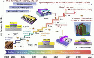
Fig. 1. Evolution of transistor density and gate length in ICs.
Definition and backgroundThe etching process involves removing a material from a surface through chemical or physical methods, which typically plays a key role in semiconductor manufacturing. Precise control of this process, including major factors such as etch depth, etch profile, surface roughness, and uniformity, is critical to ensuring the performance and reliability of micro- and nanoelectronic devices. Wet etching, which utilizes a chemical reaction in a bath environment, is known for its low cost, ease of implementation, and high material selectivity. Conversely, dry etching is performed through physical and chemical reactions in a vacuum chamber, providing greater precision depth control, profile selectivity, and the ability to define critical feature dimensions.
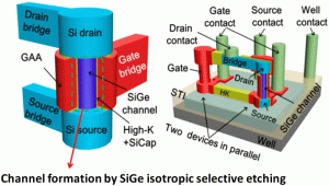
Atomic layer etching (ALE)ALE is a highly precise technique critical for fabricating nanoscale semiconductor devices. By alternating between adsorption and reaction steps, ALE achieves the removal of single atomic layers per cycle, providing exceptional control and minimizing surface roughness. This method, derived from ALD techniques, involves sequential exposure to different reactive gases, with intermediate purging steps to ensure precise layer-by-layer removal and maintain atomic-scale accuracy. ALE is particularly advantageous in the fabrication of advanced 3D integrated circuits (3D ICs) and memory devices. In 3D IC manufacturing, ALE addresses the challenges of creating complex 3D transistor architectures, such as GAA and multi-bridge-channel FETs (MBCFETs). By enabling atomic-scale etching, ALE provides exceptional control over morphology and depth, ensuring precise patterning for nanoscale features.
Neutral-beam etching (NBE)NBE represents a significant advancement in the etching processes for GaN-based HEMTs and light-emitting diodes (LEDs). This method effectively addresses the critical challenge of plasma-induced damage, which is prevalent in conventional etching techniques such as ICP-RIE. GaN materials are highly valued in the semiconductor industry for high-power and high-frequency applications. However, achieving normally-off operation in GaN-based HEMTs remains challenging due to the plasma-induced damage associated with techniques such as gate recessing. NBE offers a potential solution to minimize such damage and enhance device performance.
Deposition techniquesThin film technology is an advanced approach aimed at improving the structural, electrical, magnetic, optical, and mechanical properties of bulk materials. It has found widespread application in semiconductor devices, integrated circuits, transistors, liquid crystal displays, light-emitting diodes, solar cells, sensors, and micro-electromechanical systems (MEMSs). The distinctive properties of thin film materials are crucial for the technological advancement of various electronic, electrical, magnetic, and optical devices. These films are created using various physical or chemical methods, each of which is essential for producing ultra-thin materials known for their uniform, conformal, and controllable thickness. As atomic and near-atomic scale manufacturing (ACSM) evolves, the necessity of depositing high-quality, impurity-free thin films for laminated structures becomes crucial.
The future of ALD, ALE, and NBE technologies is promising as ongoing advancements continue to address the evolving demands of semiconductor manufacturing. Numerous optimization strategies have been employed to enhance their precision and efficiency. In particular, controlling deposition thickness in ALD, achieving atomic-level etching with ALE, and minimizing surface damage through NBE have proven crucial for improving device performance. Geometrical parameters such as layer thickness, etch depth, and surface passivation have significant impacts on device reliability and durability. Addressing thermal management, particularly in high-power applications, becomes essential as devices scale further. Future efforts could explore the use of more thermally conductive substrates and the refinement of etching profiles to minimize defects and improve device performance. Additionally, optimizing contact technologies to reduce resistance and ensure smooth surface morphology will be critical. Looking ahead, further research should focus on enhancing the uniformity and precision of these processes for advanced applications in micro-LEDs, high-speed communications, and optoelectronics. Future research should consider the performance capabilities of ALD, ALE, and NBE technologies to promote the development of next-generation semiconductor devices.
The post Advances in core technologies for semiconductor manufacturing appeared first on ELE Times.
UP Cabinet Amends 2024 Semiconductor Policy to Boost Investment
The state cabinet on Wednesday approved an amendment to the state’s Semiconductor Policy-2024 to fine-tune and adapt it to specific needs under the India Semiconductor Mission. Officials said the amendment would provide greater flexibility to investors. An official said that the move would accelerate the establishment of semiconductor units, support India’s efforts to build a domestic semiconductor ecosystem, and reduce dependence on imports of critical eleсtronic components. An official spokesperson said that the changes were aimed at providing policy support for investors and aligning the framework with the Centre’s India Semiconductor Mission. The Semiconductor Policy-2024 was notified on Jan 19, 2024, and will remain in force for five years. Officials said that the amendments would not entail any additional financial burden on the state exchequer.
The post UP Cabinet Amends 2024 Semiconductor Policy to Boost Investment appeared first on ELE Times.
Kyocera to acquire Ushio’s laser diode business
Atomera’s MST-enabled GaN-on-Si devices reduce parasitic interface charge by order of magnitude
Covalent expands wafer-level characterization through Oxford Instruments collaboration
КПІшники — серед переможців Всеукраїнської олімпіади з опору матеріалів

Студенти КПІ ім.Ігоря Сікорського найкращі серед 30 студентів із 18 закладів вищої освіти різних міст України. Вітаємо переможців серед студентів другого курсу:
Співпраця з Державною інспекцією архітектури та містобудування України

Підготовка фахівців для відбудови країни, розвитку державних інституцій та сучасної міської інфраструктури. КПІ ім. Ігоря Сікорського співпрацюватиме з Державною інспекцією архітектури та містобудування України.
ElementUSA and Colorado School of Mines awarded $67m by DOE for construction of rare-earth processing plant
Mitsubishi Electric to ship 5th-generation trench SiC MOSFET bare die samples
Homemade PCB with UV mask
 | Finally! I made a perfect pcb on a CNC with a UV mask 🔋. I really love how the copper looks under the mask. [link] [comments] |
Благодійна платформа КПІ ім. Ігоря Сікорського

КПІ ім. Ігоря Сікорського запускає charity.kpi.ua — благодійну платформу для відновлення інфраструктури, підтримки студентів, розвитку науки та збереження найбільшого технічного університету України.
Texas Instruments changes ICs without changing the part number
Hi,
I just encountered this issue with the LP2981 LDO - TI moved to a new fab and "improved" the specs but did not change the ordering code. Seems like you can only identify the difference by some characters on the reel.
Others had the same issue and now even EEV Blog talks about it... with the same issue on a different part.
I only noticed a slight difference on the print of the LP2981 while trying to find out why 80% of the new batch of PCBs are failing.
This seems like an issue with multiple components from TI, so watch out....
[link] [comments]
Memory card interfaces keep pace with the internal bus evolution race: Part 1

Clock speeds get faster. Per-cycle (and per-clock edge) address and data dollops get larger. And protocols get more efficient. But here we’re talking about external, not internal, buses.
Back in 2023, I devoted two blog posts’ worth of content to comparing various memory card technologies, products and speed bin options, initially in March (identifying a fake card in the process) and more in-depth in July. Since then, I’ve come across numerous examples of both evolutionary and revolutionary successors to the devices discussed in that two-part series, not to mention those covered in even more distant-past writeups (themed, for example, around the cameras, digital audio recorders and other devices that leverage such storage).
I’ve had this follow-up piece in my to-do list for a while now, and I’ve finally decided to actualize my longstanding aspiration before the dust pile accumulating on this specific list entry gets any deeper. Not every technology to be discussed in the paragraphs to follow will likely achieve high-volume market success, mind you, with any sooner-or-later failures not necessarily the result of implementation shortcomings, either. Note, for example, that today’s (and past) industry supply constraints encourage manufacturers to “double down” on maximizing the output and profitability of existing approaches, versus devoting scarce capacity to dubious bets.
That said, win or lose there’s usually an interesting story behind each approach. Without further ado…and with the upfront qualifier that I’ll be intentionally delaying any discussion of USB-interface memory devices until later, since their connector locations compel them to be fully external to the system, either sticking straight out of it or cable-tethered to it…and that for related reasons, I won’t be covering eMMC and other fully internal formats, either…and lastly, that I’ll be skipping over legacy formats that were proprietary and/or otherwise non-impactful…
Historical precedentsA short writeup, “History Repeating” at Virginia Tech’s website, begins as follows:
Variations on the repeating-history theme appear alongside debates about attribution. Irish statesman Edmund Burke is often misquoted as having said, “Those who don’t know history are destined to repeat it.” Spanish philosopher George Santayana is credited with the aphorism, “Those who cannot remember the past are condemned to repeat it,” while British statesman Winston Churchill wrote, “Those that fail to learn from history are doomed to repeat it.”
Long-time readers may recall that I’ve referenced variants of this same quote theme in several past writeups, consistently with a negative connotation involving the downsides of ignorance to the past. That said, excessive dependence on history lessons can also be problematic, resulting in evolutionary, overly constraining baby-steps that suppress alternative more revolutionary strides, which may lead to failure but may also dramatically leap beyond traditional approaches.
I’ll leave you to decide for yourselves what to conclude from this first case study, admittedly too personal to likely allow me to be completely arms-length about it! Embedded within the tuple (card identifier) data structures reported by Intel’s Series 2 flash memory cards were the initials of the small team of developers, myself among them, who designed their ASIC (30 years ago…yikes!). I subsequently led the technical marketing launch of the 28F008SA 8 Mbit flash memories inside those same cards, followed by the definition, development and introduction of 16 and 32 Mbit component successors and cards based on them, all in the early-to-mid-1990s.
Products such as these, representing the industry’s first removable and high capacity (for the era, at least) memory cards, added these tuple structures and other enhancements in order to deliver full Personal Computer Memory Card International Association (PCMCIA, later known as PC Card) compatibility, in contrast to Series 1 precursors which were more elementary multi-component arrays along with address decode and chip select logic. Intel’s and others’ similar products were specifically referred to as linear flash memory PC Cards, both to differentiate them from other PCMCIA card types—modems, ISDN and SCSI, for example, and living on (at least to a degree) with CableCARDs—and from alternative ATA-interface flash memory cards.

The key difference between the two memory card types centered on where the flash media management intelligence was located: in the card itself for ATA flash PC Cards, thereby presenting a standardized hardware and software interface to the system regardless of what (and whose) media was inside, versus in the system, implemented as software and/or dedicated hardware, for the linear flash PC card approach. Proponents of the latter scheme touted its claimed reduced media bill-of-materials cost, not to mention the potential ability to direct-execute code out of it (acting as a big parallel-interface chip), but it was inherently relevant for only NOR (vs NAND) memory suppliers, along with being a “heavier lift” for system developers. For these and other reasons, the ATA approach eventually won out in the marketplace.
MiniaturizationThat said, Intel and several of its NOR flash memory partner/competitors had also taken a stab at miniaturizing the linear flash PC Card with the creatively named (ha!) Miniature Card format:

Other flash memory suppliers countered with the ultimately much more popular CompactFlash card, now maintained by the aptly named CompactFlash Association (CFA), whose hardware interface was similarly PCMCIA-derived albeit instead (as with the ATA flash PC Card precursor) focused on the IDE/ATA (and later, UDMA) command set:

Amid this “where is the media management intelligence best located” debate, two other notable contending approaches of the same timeframe also bear mentioning. The first, SmartMedia, was championed by Toshiba (as well as, later, by its primary competitor, Samsung):

SmartMedia was essentially a single (although a few variants embedded multiple) NAND flash memory die embedded within a thin plastic membrane, plus a multi-contact metallic interface that wirebond-direct-connected to the die with no intervening media controller intelligence.
Conceptually sounds like linear flash PC Cards and their derivatives, doesn’t it? Yes…and no. For one thing, SmartMedia was much smaller than either Miniature Card or Compact Flash. For another, it was based on NAND flash memory, which was more HDD-like in its core attributes (notably erase block size and speed) than NOR, simplifying system-side media management development. And then there was the fact that Toshiba wasn’t just a semiconductor supplier; its various systems divisions were potential SmartMedia implementers, and the company also did a good job of cultivating business from other Japanese and broader Asian systems manufacturers.
Finally, near the end of the last century (in 1997, to be exact), Sandisk and systems partners Siemens and Nokia unveiled the MultiMediaCard (MMC), which ultimately came in multiple dimension options, as well as in both standard and clock-boosted performance variants:

MMC is best known today in its aforementioned non-removable eMMC form, which itself is being slowly supplanted by the embedded variant of the MIPI- and SCSI-based Universal Flash Storage (UFS) (an organization whose own removable-version standard ironically has conversely been underwhelmingly adopted by the industry). Today’s generational successor to MMC is the Secure Digital (SD) card, originally referred to as SecureMMC:

which built on the MMC foundation with “enhancements including a digital rights management (DRM) feature, a more durable physical casing, and a mechanical write-protect switch.” The SD standard’s successive iterations have expanded the available clock speed, protocol and electrical contact count options in a backwards-compatible fashion to keep pace with flash memory performance gains, such as in this high-end V90 card from OWC:

The microSD Card derivative tackled substantive dimensional decreases with notable success; here’s one alongside the SmartMedia card I showed you earlier:

One interesting newer SD (and microSD) card specification variation that I became aware of recently when shopping for storage media for a couple of new Raspberry Pi cards is the Application Performance Class. Quoting from Kingston Technology documentation:
A new classification has been presented with the introduction of Android’s Adopted Storage Device feature. The App Performance Class assures minimum random and sequential performance speeds to meet both run and store execution time requirements under given conditions. It does this simultaneously while providing storage for pictures, videos, music, files and other important data. Basically, they’re ideal for use in smartphones and mobile gaming devices that run applications at random read and write speeds while also being used for storage.
There are two ratings for the App Performance Class which are known as A1 and A2. A1 has a minimum random read of 1500 IOPS and a minimum random write of 500 IOPS while A2 has a minimum random read of 4000 IOPS and a minimum random write of 2000 IOPS. Both A1 and A2 have a minimum sustained write speed of 10MB/s. The App Performance Class is something to consider [editor: for example] when planning on installing Android apps on a microSD card.
And, by the way, unlike the SmartMedia competitor of the day, both MMC and successor SD Cards notably also embed (despite their smaller sizes) media management intelligence that simplifies and standardizes the system implementation. Moore’s Law strikes again, eh?
Hang tight; I’ll be right backBelieve it or not, I originally envisioned this being, and wrote it as, a single unified blog post. However, as thought of more (and more…and more…) things to include, the wordcount grew (and grew…and grew…), transforming it into something resembling a small book (I exaggerate, but you get my drift). Having passed through 1,500 words at the beginning of this paragraph, I’m instead going to pause for now, intending (God willing) to share the other half of this now-two-part series with you next week. Until then, please share in the comments your thoughts on what I’ve covered so far!
—Brian Dipert is the associate editor, as well as a contributing editor, at EDN.
Related Content
- Memory cards: Specifications and (more) deceptions
- SD card speeds: question your assumptions
- AI boom and the politics of HBM memory chips
The post Memory card interfaces keep pace with the internal bus evolution race: Part 1 appeared first on EDN.
RTX’s Raytheon awarded $515m contract for GaN-based SPY-6 family of radars
AI data-center expansion to drive monthly capacity of EML and CW-DFB lasers to 50.7 million in 2026
Murata Introduces World’s First 2.2μF/100Vdc Soft-Termination Chip MLCC in 0805-inch Size for Automotive Applications
Murata Manufacturing Co., Ltd. introduces the GCJ21BD72A225KE02, a soft-termination chip multilayer ceramic capacitor (MLCC) for automotive powertrain and safety equipment. This world’s first soft-termination chip MLCC product achieves the highest available capacitance of 2.2μF at 100Vdc in the smallest 0805-inch (2.0×1.25mm) size.
As vehicle electrification accelerates and autonomous driving (AD) and advanced driver-assistance systems (ADAS) grow more sophisticated, engineers face increasing pressure to pack more functionality into tighter board spaces. The wider adoption of 48V power systems further demands components that combine high capacitance, high voltage tolerance, and a small footprint. At the same time, mechanical stress from board flexure, due to vibration and thermal cycling while driving, remains a reliability concern. The GCJ21BD72A225KE02 addresses all these challenges.
Built on Murata’s proprietary ceramic material design, including fine particle size and uniformity control, the soft-termination chip MLCC achieves 2.2μF at 100Vdc in the 0805-inch size, a rating previously only possible in the larger 1206-inch (3.2×1.6mm) size. The result is an approximately 51% reduction in board mounting area compared to Murata’s previous 2.2μF/100Vdc offering, and an approximately 2.2x increase in capacitance over its previous 0805-inch, 100Vdc product. Soft termination further enhances field reliability by absorbing board flexure stress and reducing post-mount cracking.
The GCJ21BD72A225KE02 supports an operating temperature range of -55°C to +125°C and meets X7T temperature characteristics per EIA standards. Murata will continue expanding its automotive-grade MLCC lineup, delivering the miniaturization, high capacitance, high voltage ratings, and reliability that next-generation vehicles demand.
The post Murata Introduces World’s First 2.2μF/100Vdc Soft-Termination Chip MLCC in 0805-inch Size for Automotive Applications appeared first on ELE Times.
Сторінки



