
Збирач потоків
GaN ICs drive robotics and motion control

Four 100-V GaN power-stage ICs from EPC are optimized for motor drives in humanoid robots, drones, and battery-powered platforms. The EPC23108, EPC23109, EPC23110, and EPC23111 integrate a gate driver, high- and low-side eGaN FETs, and level-shifting circuitry in a half-bridge configuration. They support operation up to 100 V with load currents of 35 A (EPC23108, EPC23109) and 20 A (EPC23110, EPC23111).

The control interface includes an active-low fast-shutdown and standby input with a 65-kΩ pull-up. It meets industrial logic standards, letting designers connect directly to standard controllers. This simplifies designs and ensures consistent operation across platforms. Safety is enhanced through deterministic shutdown.
The series supports continuous 100% duty-cycle operation, enabling full-torque and uninterrupted conduction in motion control, robotics, and precision regulation systems. The EPC23109 and EPC23111 offer a single-pin PWM input with enable logic and fixed dead time, simplifying multi-axis designs. The EPC23108 and EPC23110 feature dual PWM inputs for adaptive dead-time modulation.
Engineering samples are available for qualified designs. The EPC23108, EPC23109, EPC23110, and EPC23111 can be ordered through EPC’s distributor partners.
The post GaN ICs drive robotics and motion control appeared first on EDN.
Tiny filters curb 5-GHz audio-line noise

Built with low-distortion ferrite material, TDK’s MAF0603GWY series of filters attenuates noise on audio lines in the 5-GHz band. The filters fit in a compact 0.6×0.3×0.3-mm package for use in small consumer devices like smartphones and wearables with Bluetooth and Wi-Fi audio lines.

Electromagnetic noise radiated from audio lines in electronic devices can interfere with the internal antenna and reduce receiver sensitivity. While chip beads are commonly used to suppress noise, they can degrade sound quality.
TDK reports its newly developed ferrite material minimally affects audio-line characteristics while reducing distortion. The filters provide high attenuation at 5 GHz (impedance up to 3220 Ω) to suppress noise. They also limit attenuation of audio signals with lower resistance than conventional products, enabling a wide dynamic range.

Mass production of the MAF0603GWY series is set to begin in April 2026.
The post Tiny filters curb 5-GHz audio-line noise appeared first on EDN.
Photovoltaic driver streamlines EV power designs

A photovoltaic MOSFET driver from Vishay, the VODA1275 increases safety and reliability in high-voltage automotive applications. The device provides a typical open-circuit voltage of 20 V, short-circuit current of 20 µA, and turn-on time of 80 µs—said to be three times faster than competing devices.

The AEC-Q102-qualified device targets pre-charge circuits, wall chargers, and battery management systems for EVs and HEVs. Its high open-circuit output voltage allows a single driver to be used, removing the need for two devices in series to generate higher voltages. The VODA1275 also enables custom solid-state relays to replace electromechanical relays in next-generation vehicles.
A working isolation voltage of 1260 Vpeak and isolation test voltage of 5300 VRMS make the driver well-suited for 800-V+ battery systems. The device comes in a compact SMD-4 package with an 8-mm creepage distance and a mold compound with a CTI of 600.
Samples and production quantities of the VODA1275 are available now, with lead times of eight weeks.
The post Photovoltaic driver streamlines EV power designs appeared first on EDN.
Shielded inductors reduce emissions in tight layouts

Bourns’ SRP2008DP series of shielded power inductors provides the saturation current needed for dense DC/DC converter designs and miniature electronic devices. These low-profile devices, with dimensions of just 2.0×1.6×0.8 mm, enable use in compact circuits with minimal routing changes.

The eight inductors in the SRP2008DP series cover inductances from 0.24 µH to 4.70 µH, heating current (IRMS) from 1.10 A to 3.50 A, and saturation current (ISAT) from 1.60 A to 5.50 A. DC resistance ranges from 36 mΩ to 468 mΩ, and operating temperature spans -40°C to +125°C.
In crowded layouts, radiated emissions and magnetic coupling can compromise signal integrity and complicate EMC compliance. The SRP2008DP series addresses these issues with a small, shielded package and a metal-alloy powder core. The shielded design contains magnetic flux, reducing emissions to nearby circuitry, while the high-resistivity core suppresses eddy currents and limits core losses at high switching frequencies. Contained flux also minimizes coupling to adjacent traces, lowering interference in densely populated layouts.
The SRP2008DP series is available through Bourns’ authorized distributors. Request samples here.
The post Shielded inductors reduce emissions in tight layouts appeared first on EDN.
RISC-V SoC supports voice-enabled IoT devices

Espressif Systems is sampling its ESP32-S31 dual-core RISC-V SoC with Wi-Fi 6, Bluetooth 5.4, Thread, Zigbee, and Ethernet. Rich HMI and security features make it well-suited for IoT applications such as consumer and industrial appliances, voice-controlled devices, and automation systems.

Running at 320 MHz, the ESP32-S31’s 32-bit RISC-V microcontroller achieves 6.86 CoreMark/MHz and integrates a memory management unit and 60 GPIOs for design flexibility. One of its two cores features a 128-bit-wide SIMD data path for fast parallel processing. Memory resources comprise 512 KB SRAM and support for 250-MHz, 8-bit DDR PSRAM, with concurrent flash and PSRAM access. External memory expansion (up to octal SPI) further supports memory-intensive multimedia and AI/ML workloads at the edge.
The ESP32-S31’s HMI capabilities include a DVP camera interface, LCD support, and up to 14 capacitive touch channels. Security features span secure key management, secure boot, flash and PSRAM encryption, cryptographic hardware acceleration, and a trusted execution environment. Supported by Espressif’s open-source IoT Development Framework, the device works with common LLMs to build voice-enabled client devices that run or interact with AI agents.
To request samples of the ESP32-S31 SoC, contact Espressif’s customer support team.
The post RISC-V SoC supports voice-enabled IoT devices appeared first on EDN.
Leveling up Industry 4.0

Industry 4.0 is all about transforming manufacturing processes with advances in smart capabilities, data connectivity, and automation. It encompasses devices from sensors that capture data to motors and motor control and power devices that have a big impact on efficiency. Edge computing is also playing a larger role to combat challenges around latency, particularly in safety critical applications, and cybersecurity is critical for protecting connected devices.
 (Source: Adobe Stock)
The March/April issue covers some of the key components that are vital to Industry 4.0, from new sensing approaches such as event-based sensing that enable faster and more reliable decisions to the latest designs in power devices to deliver higher efficiency in industrial systems. We also look at designing edge AI for industrial and industrial IoT systems for cybersecurity.
Machine vision plays a big role in industrial automation applications, ranging from object tracking to vibration monitoring. Prophesee believes the industry should be rethinking machine vision in industrial automation, addressing challenges around latency, data processing, and decision-making.
“As industrial systems move toward higher levels of automation and autonomy, vision is becoming a core component of the perception pipeline,” said Thibaut Willeman, head of business development and go-to-market at Prophesee.
This is driving the demand for new sensing approaches that address these challenges: reducing latency, limiting unnecessary data, and enabling faster and more reliable decisions, he added.
Willeman explains how event-based vision addresses these challenges: “By mimicking biological vision, this technology utilizes efficient sensing and collection techniques that capture changes within a specific scene. This reduces processing requirements compared with traditional frame-based methods while revealing details that conventional systems miss, opening new possibilities for precision and performance in industrial applications.”
Applications that can benefit from event-based vision include industrial automation, IoT, automotive, and edge applications.
Another component area that has a large impact on applications in the Industry 4.0 world is power electronics. As factories, energy systems, and data centers get smarter and more connected, it requires more efficient power solutions that offer high power density, said Stefano Lovati, contributing writer.
Lovati discusses some of the latest approaches to designing, packaging, and controlling power devices to deliver higher efficiency, flexibility, and scalability. One of the most significant changes introduced in the power system is the move to 800-VDC distribution in data centers.
There is also a key focus on wide-bandgap materials such as silicon carbide (SiC) and gallium nitride (GaN). SiC can operate efficiently and provide high reliability in high-voltage and high-power environments, thanks to its high breakdown voltage, low switching losses, and high thermal conductivity, while GaN, suited for low- and medium-voltage applications, can switch at high frequencies, up to the megahertz range, with very low power loss, making power converters more efficient and smaller and requiring less cooling, Lovati said.
In addition, GaN is delivering on integration, which is helping to simplify power design.
Another big element of implementing smart manufacturing within Industry 4.0 is motor control ICs and motor drives. Similar to power devices, a big challenge is efficiency. “About 50% of global energy consumption is due to electric motors, and therefore, even a moderate improvement in efficiency can provide meaningful economic benefits, helping reduce the carbon footprint,” Lovati reports.
These modern industrial motor solutions are smart and connected with advanced capabilities to identify irregularities such as excessive heat or voltage surges and respond automatically. Lovati said the introduction of AI technologies brings this function to the next level, allowing predictive maintenance and reducing factory downtime.
He covers everything from motor driver architecture and connectivity in smart motor control to AI and ML integration and software tools.
Edge computing is becoming critical for real-time data processing in industrial automation. Industrial manufacturing systems require real-time decision-making, adaptive control, and autonomous operation, but many cloud-dependent architectures can’t deliver the millisecond response required for safety-critical functions such as robotic-collision avoidance, in-line quality inspection, and emergency shutdown, said Sam Al-Attiyah, head of machine learning at Infineon Technologies AG.
Al-Attiyah said edge AI addresses high-performance and low-latency requirements by embedding intelligence directly into industrial devices and enabling local processing to support machine-vision workloads for real-time defect detection, adaptive process control, and responsive human-machine interfaces that react instantly to dynamic conditions.
He outlines an approach to designing edge AI systems for industrial applications, covering everything from requirements analysis to deployment and maintenance.
Security is also a growing concern and an industry requirement as more devices are connected in industrial environments. Francesco Vaiani, senior product manager at Seco, looks at how designing for industrial IoT systems is changing to meet the European Cyber Resilience Act and the cybersecurity extension of the Radio Equipment Directive. This marks a structural shift in how connected products must be designed, documented, and maintained, he said.
For industrial OEMs, this means more than documentation updates and demands architectural decisions that remain technically defensible throughout the operational lifetime of the device, which often exceeds 10 years, Vaiani said.
Also in this issue, we select the top 10 DC/DC converters introduced over the past year. DC/DC converter manufacturers continue to focus on two big areas: delivering higher efficiency and offering greater flexibility.
Don’t miss the APEC 2026 product roundup. This annual conference showcases the latest in power electronics devices and solutions across industries. Some of these power devices highlight major technology advances in areas such as topologies and packaging, along with meeting growing demand for higher efficiency and higher power density. They also address system complexity by helping to simplify power design.
The post Leveling up Industry 4.0 appeared first on EDN.
Finally nailed down my homebrew PCB fab process (see photos)
") | The photos are:
Over all I'm very happy with how it turned out. The main thing I'm unsure of at the moment is whether I should leave the paint on the traces or not. I figured it would provide some protection against corrosion, but as you can tell it's pretty fragile and has already been scraped off in several places. I might still just clean it all off. [link] [comments] |
METCASE expands accessory options for enclosures

METCASE’s new enclosure accessories brochure features its expanded range of options including metal tilt/swivel bail arms, a wide range of molded enclosure feet, PCB mounting parts, 19″ front panels, rack shelves and rack hardware.
 (Source: METCASE USA)
These universal accessories fit METCASE models and other manufacturers’ enclosures, as well as bespoke OEM equipment housings. Applications include networking, communications, laboratory instrumentation, industrial control, test/measurement, peripherals, interfaces and medical devices.
Bail arms with 30° indexing double as desk stands. The aluminum handle profile (ordered separately) fits between two diecast side arms. It is supplied cut to the required length for the customer’s enclosure. The bail arms are available in a range of color combinations including off-white, anthracite, light gray, black and traffic white.
METCASE’s recently expanded range of molded ABS (UL 94 HB) enclosure feet kits can be specified with/without tilt legs. They are suitable for metal and plastic enclosures. There are two models: robust CASE FEET and the designer TECHNOFEET. The feet are easy to fit (just three holes required) with the fixing screws supplied. TPE non-slip inserts are included to prevent the enclosure skidding on the desk. Choose from five standard colors: off-white, traffic grey A, light gray, black and anthracite.
For mounting circuit boards, METCASE offers a range of snap-in guides (for slide-in PCB fitment) in different lengths and for board thicknesses from 0.031″ to 0.078″. For screw fitting PCBs to enclosure panels, there is a kit that includes M3 PCB pillars (0.394″ high) and mounting hardware.
METCASE also offers a range of accessories for 19″ racks. This includes matt anodized aluminum 10.5″/19″ front panels (ventilated/unventilated) in all standard heights from 1U to 6U; the 10.5″ front panels are 3U and 4U. There are also mild steel CR4 2U cantilever rack shelves for mounting equipment without rack brackets. Choose from two depths 11.02″/15.75″ in light gray or anthracite. 19″ equipment mounting kits include four bolts, four cup washers (black or gray) and four caged nuts.
For further information, view the METCASE website and download the accessories brochure: https://www.metcaseusa.com/en/Accessories/Accessories-for-Enclosures.htm
The post METCASE expands accessory options for enclosures appeared first on EDN.
🖼️ Запрошуємо на виставку «Міська мозаїка» Лариси Пуханової

🖼 У Державному політехнічному музеї КПІ ім. Ігоря Сікорського відкрили виставку «Міська мозаїка» Лариси Пуханової. Це персональна виставка відомої київської художниці, яка має унікальну мистецьку мову, витончений смак і впізнаваний стиль. Її творчість — чуттєва, захоплива й жива.
Advancing AI performance with HBM4, SPHBM4 DRAM solutions

Over the past two decades, the raw compute capability of processors used in high‑performance computing (HPC) and artificial intelligence (AI) systems has increased at an extraordinary pace. Figure 1 illustrates this trend: XPU floating‑point performance has scaled by more than 90,000×, while DRAM bandwidth and interconnect bandwidth have improved by only about 30× over the same period.

Figure 1 The above chart highlights increases in XPU performance and interconnect bandwidth over 20 years.
This growing disparity between compute capability and data movement—often described as the memory wall and the I/O wall—has become one of the most significant constraints on achievable system performance.
For system designers, this imbalance translates directly into underutilized compute resources, rising power consumption, and increasing architectural complexity. As a result, memory bandwidth and packaging technologies have become just as critical to AI performance scaling as transistor density or core count.
HBM as a foundation for modern AI architectures
To address these bandwidth challenges, HPC and AI systems have increasingly adopted disaggregated architectures built around chiplets. While LPDDR and DDR memories continue to play important roles, high bandwidth memory (HBM) has emerged as the highest‑bandwidth DRAM solution available and a key enabler for modern accelerators.
HBM devices consist of a buffer (or base) die at the bottom and multiple 3D‑stacked DRAM layers above it. The buffer die uses very fine‑pitch micro‑bumps, allowing the memory stack to be co‑packaged with an ASIC using advanced packaging technologies such as silicon interposers or silicon bridges. Supported by rigorous standardization through the JEDEC HBM task group, HBM has become one of the most successful and widely adopted examples of chiplet‑based integration in production systems.
Figure 2 shows a representative side view of an HBM DRAM stack connected to an ASIC through a silicon interposer.

Figure 2 Here is how an HBM DRAM stack is connected to an ASIC through a silicon interposer. Source: Eliyan
A widely deployed example of HBM in practice is Nvidia’s B100 Blackwell accelerator, shown in Figure 3. The package contains two large, reticle‑sized XPU dies connected to one another through high‑bandwidth links, with HBM devices placed along the top and bottom edges of each die. Each XPU die integrates four HBM stacks—two on each long edge—resulting in a total of eight HBM devices per package.

Figure 3 Nvidia’s B100 Blackwell accelerator uses two XPUs connected to eight HBMs in a single package. Source: Nvidia
Using typical HBM3 specifications available at the time the JEDEC standard was adopted, each HBM3 device could employ an 8‑high stack of 16-Gb DRAM layers, providing 16 GB of capacity per stack. With a data rate of 6.4 Gb/s and 1,024 I/Os, each HBM3 device delivers approximately 0.8 TB/s of bandwidth. Across eight devices, this configuration provides 128 GB of total memory capacity and roughly 6.6 TB/s of aggregate bandwidth.
HBM4: Scaling bandwidth and capacity
To continue scaling memory performance alongside compute, JEDEC recently published JESD270‑4, the HBM4 standard. HBM4 introduces a number of architectural improvements over HBM3 that directly address the growing bandwidth and capacity requirements of AI workloads.
One of the most significant changes in HBM4 is a doubling of the channel count, increasing the number of I/Os from 1,024 to 2,048. In parallel, supported data rates have increased into the 6–8 Gb/s range and beyond. Memory density has also scaled, with 24 Gb and 32 Gb DRAM layers specified, along with support for 12‑high and 16‑high stacks. Reliability, availability, and serviceability (RAS) features—including DRFM—have also been enhanced.
Taken together, these advances enable substantial improvements in bandwidth, power efficiency, and capacity relative to HBM3. As an illustrative example, an HBM4e device using a 16‑high stack of 32 Gb layers provides 64 GB of capacity per device, as shown in Figure 4.

Figure 4 Eight HBM4 devices are shown in an example package accomplishing increased total capacity and bandwidth. Source: Eliyan
With 2,048 I/Os operating at 8 Gb/s, such a device can deliver up to 2 TB/s of bandwidth. In a package containing eight HBM4 devices, total memory capacity scales to 512 GB—four times that of the earlier HBM3 example—while aggregate bandwidth exceeds 16 TB/s, a 2.5× increase.
Custom HBM and the role of the base die
As HBM4 adoption accelerates, some system designers are exploring the development of custom HBM solutions optimized for specific applications. A key enabler of this trend is the evolution of the HBM base die.
In earlier HBM generations, the base die was typically manufactured using a DRAM‑optimized process, well suited for capacitor structures but less optimal for high‑speed logic. With HBM4, most suppliers are transitioning to standard advanced logic processes for the base die. This shift aligns more closely with the processes already familiar to SoC designers and opens the door to customization opportunities.
Whether using standard or custom HBM4 devices, these solutions continue to rely on advanced packaging and silicon substrates—such as interposers or bridges—to accommodate the large number of fine‑pitch connections between the memory and the ASIC.
SPHBM4: Bringing HBM‑class bandwidth to organic packaging
Despite its performance advantages, traditional HBM integration requires advanced packaging, which can increase cost and complexity. Many system designers, particularly those focused on volume production and reliability, prefer standard organic substrates. To address this gap, JEDEC has announced that it is nearing completion of a new standard for Standard Package High Bandwidth Memory (SPHBM4).
SPHBM4 devices use the same DRAM core dies as HBM4 and provide equivalent aggregate bandwidth, but they introduce a new interface base die designed for attachment to standard organic substrates. Figure 5 illustrates a side view of an SPHBM4 DRAM mounted directly on an organic package substrate, alongside an ASIC. The ASIC itself may also reside on the organic substrate, or it may remain on advanced packaging such as a silicon bridge for multi‑XPU integration.

Figure 5 Side-view of an SPHMB4 DRAM and ASIC connection is shown with the SPHBM4 DRAM attached directly to the organic package substrate. Source: Eliyan
To achieve HBM4‑class throughput with fewer pins, SPHBM4 employs higher interface frequencies and serialization. While HBM4 defines 2,048 data signals, SPHBM4 is expected to use 512 data signals with 4:1 serialization, enabling the relaxed bump pitch required for organic substrates.
Because SPHBM4 uses the same DRAM stacks as HBM4, per‑stack capacity remains unchanged. However, organic substrate routing supports longer channel lengths between the SoC and the memory, which can enable new system‑level trade‑offs. In particular, longer routing distances and angled trace routing can allow more memory stacks to be placed around a given die.
Figure 6 illustrates this effect. When HBM devices are mounted on silicon substrates, they must be placed immediately adjacent to the XPU, limiting the number of stacks to two per 25-mm die edge. With SPHBM4 on an organic substrate, three memory devices can be connected along the same edge, increasing both memory capacity and bandwidth by approximately 50%.

Figure 6 This is how 12 SPHBM4 devices in example package boost capacity and total bandwidth. Source: Eliyan
Even when a silicon substrate is still used beneath the XPU—for example, to support high‑bandwidth XPU‑to‑XPU links—the overall interposer size can be significantly reduced when memory devices are moved to the organic package. This reduction can translate into meaningful benefits in system cost, manufacturability, and test complexity.
Looking ahead
AI workloads continue to push the limits of memory bandwidth, capacity, and packaging technology. JEDEC’s HBM4 standard represents a major step forward in addressing these demands, while the emerging SPHBM4 standard expands the design space by enabling HBM‑class performance on standard organic substrates.
For system architects, these technologies offer new flexibility in balancing performance, cost, and integration complexity. As memory and packaging increasingly shape overall system capability, early consideration of options such as HBM4, custom HBM, and SPHBM4 will be essential to fully unlocking the next generation of AI and HPC performance.
Kevin Donnelly is VP of strategic marketing at Eliyan.
Related Content
- What the special section on chiplets design has to offer
- Chiplet innovation isn’t waiting for perfect standards
- Scoping out the chiplet-based design flow
- Demystifying 3D ICs: A practical framework for heterogeneous integration
- Chiplets: 8 best practices for engineering multi-die designs
- Overcoming interconnect obstacles with co-packaged optics (CPO)
The post Advancing AI performance with HBM4, SPHBM4 DRAM solutions appeared first on EDN.
HRL’s T3L 40nm GaN-on-SiC technology achieves Manufacturing Readiness Level 6
Rethinking machine vision in industrial automation

Machine vision has always played a critical role in ensuring safe, efficient, and reliable operation in many industrial settings. However, as vision-enabled machines become more numerous and the type and volume of data they can collect expand, challenges are forcing system makers to look at new approaches to efficiently acquire, process, and utilize visual data.
If we look at the current challenges, they span the spectrum in terms of improving operational efficiency, accuracy, and reliability.
Data overload and processing efficiency that limits throughput are major issues as industries move toward more advanced, faster automation, tasking vision systems with capturing and analyzing vast amounts of data. Traditional vision systems often struggle with the sheer volume of images they capture, much of which can be redundant. The requirement now is not just about capturing high-resolution images but doing so in a way that first and foremost accelerates throughput (in part by minimizing irrelevant data) while maximizing the precision and relevance of the information captured.
Real-time processing is becoming increasingly important, especially in environments where machines need to make instantaneous decisions, such as in quality control or defect detection on production lines. This requires more efficient processing methods and data reduction techniques.
High-speed and high-precision demands increase as production lines get faster. High-speed processing, low latency, and the ability to capture minute changes in a scene in real time are critical. Traditional frame-based systems struggle with motion blur and data overload when capturing fast-moving objects. For example, in applications such as high-speed counting, even the slightest delay in image acquisition and processing can lead to errors.
Sustainability is a growing priority, as many industrial systems operate in environments where power efficiency is key. Vision systems need to operate for extended periods without consuming significant amounts of energy. Traditional image-processing systems, especially those that capture entire frames at a fixed rate, can be power-intensive and require sophisticated cooling or energy management.
Complex lighting and environmental conditions are common in many settings, including extreme brightness, low light, or dynamic lighting scenarios. Vision systems need to cope with high-dynamic-range requirements to capture high-quality images without losing detail in either the darkest or brightest areas. Conventional frame-based systems have struggled in such conditions, leading to the need for more adaptable and sensitive vision technologies.
Predictive maintenance and condition monitoring are growing needs. Vision systems must not only react to issues but also help to predict potential problems before they occur. Predictive maintenance requires vision systems that can monitor machine vibrations, detect wear and tear, and identify early signs of equipment failure.
These challenges point to a more fundamental limitation: Traditional frame-based vision was designed for image capture and human viewing, not for machines that must detect, interpret, and react to changes in real time. As industrial systems move toward higher levels of automation and autonomy, vision is becoming a core component of the perception pipeline.
This shift is driving demand for sensing approaches that reduce latency, limit unnecessary data, and enable faster, more reliable decisions across applications such as monitoring, inspection, counting, and control.
Event-based vision addresses these challengesEvent-based vision, inspired by the human eye and brain, is increasingly used in industrial machine vision to address these challenges. By mimicking biological vision, this technology utilizes efficient sensing and collection techniques that capture changes within a specific scene. This reduces processing requirements compared with traditional frame-based methods while revealing details that conventional systems miss, opening new possibilities for precision and performance in industrial applications.
Event-based vision is particularly suited for industrial automation, IoT, automotive, and edge applications that demand high performance, low power consumption, and operation in challenging lighting conditions. The technology offers significant advantages in speed, power efficiency, dynamic range, and low latency, driving use cases such as high-speed counting, preventive maintenance, and inspection.
From frame-based imaging to event-based perceptionIn conventional video systems, entire images (i.e., the light intensity at each pixel) are recorded at fixed intervals, known as the frame rate. Standard movies are recorded at 24 fps, with some videos using higher frame rates like 60 fps (16.7-ms intervals). While effective for representing the “real world” on a screen, this method oversamples unchanged parts of an image, especially at high frame rates, while undersampling the most dynamic areas. As a result, critical motion information can be missed between frames.
In contrast, the human eye samples changes up to 1,000× per second without focusing on static backgrounds at such high frequencies. Event-based sensing offers a biologically inspired solution to this under- and oversampling. Unlike traditional cameras, event sensors don’t use a uniform acquisition rate (frame rate) for all pixels. Instead, each pixel defines its sampling points by reacting to changes in the amount of light it detects. Information about contrast changes is encoded in “events”—data packets containing the pixel’s coordinates and the precise time of the event.
 Figure 1: Frame-based vs. event-based sensing—discrete frame sampling vs. continuous motion capture (Source: Prophesee)
Prophesee’s patented event-based sensors, for instance, allow each pixel to activate intelligently based on detected contrast changes. This enables continuous acquisition of essential motion information at the pixel level. The pixels operate asynchronously (unlike traditional CMOS cameras) and at much higher speeds, as they don’t need to wait for a complete frame before reading data.
The advantages of event sensors include high-speed operation (equivalent to 10,000 fps), extremely efficient power consumption (down to the microwatt range), low latency, reduced data processing requirements (10× to 10,000× less than frame-based systems), and high dynamic range (up to 140 dB).
Because only changes are transmitted, event-based data streams are inherently sparse and temporally precise, allowing downstream processing systems—including AI-based processing—to focus on what matters: motion, variation, and anomalies rather than static background information. These attributes make event-based vision systems suited for a wide range of applications and products.
This technology is being commercialized more widely, such as in Prophesee’s Metavision, which has evolved over the past decade to deliver high performance through integrated hardware and software solutions.
Real-time industrial automation with event-based visionEvent-based vision excels in a variety of industrial automation applications. Typical use cases (see Figure 2) range from object tracking and high-speed counting to predictive maintenance and quality control.
 Figure 2: Applications of event-based vision in industrial automation (Source: Prophesee)
Safety: Object tracking
Figure 2: Applications of event-based vision in industrial automation (Source: Prophesee)
Safety: Object tracking
Event-based vision systems excel at tracking moving objects, leveraging their low data rate and sparse information capabilities. This approach allows for precise object tracking with minimal computational resources, eliminating traditional “blind spots” between frame acquisitions. Additionally, event sensors offer native segmentation, focusing solely on movement and disregarding static backgrounds for improved tracking accuracy and efficiency. Event-based vision enhances safety by monitoring worker and machine interactions in real time, even in complex lighting, without capturing images.
Productivity: high-speed countingReal-time vision systems powered by event-based sensing enable objects to be counted at unprecedented speeds with high accuracy and minimal motion blur. Sensors independently trigger each pixel as objects pass through the field of view, achieving a throughput of over 1,000 objects per second and an accuracy of more than 99.5%, ensuring rapid and precise counting in high-speed environments.
Predictive maintenance: vibration monitoringEvent-based vision enables continuous, remote vibration monitoring with pixel-level precision. By tracking the temporal evolution of each pixel in the scene, the sensors record each event’s coordinates, polarity of change, and exact timestamp. This data provides valuable insights into vibration patterns across frequencies from 1 Hz to the kilohertz range, aiding in predictive maintenance.
 Figure 3: Event-based vibration monitoring in industrial systems; frame-based imaging shown for reference (Source: Prophesee)
Quality: particle/object size monitoring
Figure 3: Event-based vibration monitoring in industrial systems; frame-based imaging shown for reference (Source: Prophesee)
Quality: particle/object size monitoring
In high-speed production environments, event-based sensing allows for real-time control, counting, and measurement of particle or object sizes on conveyors or channels. The sensors capture instantaneous quality statistics, ensuring accurate process control at speeds of up to 500,000 pixels per second with a counting precision of 99%, optimizing quality assurance in production lines.
 Figure 4: High-speed event-based particle counting and size monitoring; frame-based image shown for reference (Source: Prophesee)
Quality control
Figure 4: High-speed event-based particle counting and size monitoring; frame-based image shown for reference (Source: Prophesee)
Quality control
Event-based vision systems help lower reject rates with real-time feedback and advanced processing down to a 5-µs time resolution and blur-free asynchronous event output. One specific use case is in the automatic detection and classification of the finest imperfections in manufacturing materials—for example, in automotive parts to perform paint defect inspection, scratch detection, and planarity testing (see Figure 5).
 Figure 5: Event-based surface contamination and defect detection in industrial production (Source: Prophesee)
As event-based vision continues to evolve and address diverse market needs, it is establishing itself as a new industry standard. Over the past several years, the technology has expanded to serve a wide array of applications.
Thousands of product developers are now adopting event-based vision for sophisticated camera and perception systems, supported by open-source technology and a growing inventors’ community. These advancements are transforming how machines perceive, process, and react to visual information in real time, bringing greater precision, efficiency, and intelligence to industrial automation operations.
Thibaut Willeman is head of business development and go-to-market at Prophesee, where he works on the market development of event-based vision systems for industrial automation, robotics, and defense applications. He previously held strategy and innovation roles at companies such as Boston Consulting Group, working on growth strategy, product strategy, and innovation initiatives for industrial and technology companies. He holds an engineering degree and a master’s degree in innovation and technology management.
The post Rethinking machine vision in industrial automation appeared first on EDN.
Humidifiers and such: How much “smart” is too much?

This engineer’s new humidifier is—he kids you not—Wi-Fi enabled, therefore “smart”. What upsides does such a product deliver? And at what tradeoffs?
Within one of last month’s writeups, I mentioned that my wife and I had recently acquired two DREO 4 liter-capacity ionizing humidifiers. That purchase led to my interest in hygrometers (humidity measurement devices) such as the TP-Link Tapo T315, which ended up supplanting the bad data I’d previously relied upon, coming from my furnaces’ touchscreen thermostats.
Ionizing advancementsThe baseline DREO HM311:
relies on front panel buttons for user control purposes. It works well, and I enjoy the dynamic bubbling-water “light show” projected through the center mist tube, particularly visible at night:

The ionizing design approach is also interesting; just make sure to remember to keep ‘em clean:

Its slightly more expensive “smart” sibling, the HM311S, adds Wi-Fi support, thereby making it controllable (and more broadly manageable) via a mated smartphone or other mobile device:

or even, courtesy of its integrated Amazon Alexa and Google Assistant support, your voice:
And the tri-color mist tube (which I’d been calling a “pillar” until I revisited the user manual just now), is a handy visual reference to the current measured humidity level (I’ve yet to see blue):
|
Light Color |
Humidity Level |
|
Yellow |
≤30% |
|
Green |
31-60% |
|
Blue |
≥61% |
Believe it or not, the HM311S is even the beneficiary of periodic firmware updates, such as the one that I was prompted to install as part of initial out-of-box setup:


Another update, I noticed, was available as I re-accessed the device via my smartphone two-plus months later, just prior to writing these words:


And yes, the humidifier’s status and settings are even accessible over the Internet; note the cellular-only connection in the following screenshot (per the reported 436 hours of use to date, this was an Amazon Warehouse-sourced, apparently previously-used unit, even though it arrived in seemingly brand-new condition):

Nifty. But also potentially (more than) a bit scary. First off, what’s the realistic benefit (if any) of remote status monitoring from my mobile device? It’s not like I have a robot sitting at home in my absence that can alternatively grab a water pitcher, fill it and transfer its contents to the humidifier if it empties, after all. Not yet, at least:

More generally, is it convenient to turn on and off (and raise and lower the output intensity) of the humidifier from the couch, using either the aforementioned smartphone or my voice? Sure. But on the other hand, I could also always use the exercise. And what do I give up in exchange for all this supposed connectivity “goodness”?
For one thing, I’m sharing WAN IP address, device usage and ambient analytics data with the manufacturer. For a humble DREO humidifier, maybe this degree of reveal isn’t such a big deal. But what about my Google Nest Wifi mesh network, similarly managed via the cloud? Or my Blink security camera setup, which leverages cloud services not only for monitoring and control purposes but also to store recordings (at least currently; stay tuned for next week’s teardown)?
And what happens if those cloud services, not only from DREO (or its Amazon Alexa partner), Google or Blink but any other similar supplier, get hacked? Sure, it’s annoying to have someone remotely switching on and off your humidifier out of your control. That time someone used my then-firewall-exposed IPP port to spit pages (and pages and pages) of gibberish out of my laser printer was a bit more annoying. But that’s not what I’m talking about when I say “scary”.
The hackers now know who I am from my account profile and can easily determine my location via an online search using my name. Since they know my WAN IP address, they can now attempt to hack me. They also know my Wi-Fi network credentials, which makes it even easier to get inside my LAN if, since they now know my location, they’re motivated to pull up and park on the street outside. They know my account username and password, which theoretically should be unique to this particular cloud service but—get real—is undoubtedly reused elsewhere. And for a paid cloud service, they also now know my credit card and/or bank account info. Fun times!
Is elementary (especially) convenience worth the potential consequences? If you’re a consumer, it’s a question you should be asking yourself pre-purchase…although you’re likely to be unaware of the possible downsides. Therefore, if you’re a manufacturer, it’s a question you should be asking on behalf of your potential customers during the initial development process…although you’ve also got marketing breathing down your neck for new features, and your competitors may have already unveiled similar capabilities, so you’re also under late-to-market pressure, so…
When, if ever, is a product too “smart”? Or taking the thought to the other end of the extremist spectrum, should products be “smart” at all, at least for the mass market? As always, I welcome your thoughts in the comments!
—Brian Dipert is the associate editor, as well as a contributing editor, at EDN Magazine.
Related Content
- The Tapo Hub: TP-Link joins the low-bandwidth, long-range RF club
- The whole-house LAN: Achilles-heel alternatives, tradeoffs, and plan
- Blink: Security cameras with a power- and bandwidth-stingy uplink
- IoT device vulnerabilities are on the rise
The post Humidifiers and such: How much “smart” is too much? appeared first on EDN.
Directed Energy Systems: Where Capability Ends and Control Begins
by Sukhendu Deb Roy, Industry Consultant
Key Takeaways- The economics of warfare have flipped, with cost asymmetry emerging as a primary battlefield dynamic
- Directed energy systems shift defence from inventory-driven models to energy-driven ones
- Future defence architectures will be AI-orchestrated, integrated, and multi-domain
- Semiconductor capability is central to defence sovereignty
Modern warfare is undergoing a structural and economic shift—one that is redefining how conflicts are fought and sustained. Across theatres, adversaries are increasingly deploying low-cost, high-volume threats designed not just to penetrate defences, but to exhaust them. This is not merely a tactical evolution; it is an economic strategy aimed directly at the cost structure of defence systems rather than their technical limits.
In response, Directed Energy Weapons (DEW), particularly high-energy laser (HEL) systems, are emerging as a compelling alternative. By reducing the cost per engagement to near-zero and removing dependence on finite ammunition, they signal a transition toward energy-based warfare—where power availability replaces inventory as the primary constraint.
Operational systems today, typically in the 100–300 kW class, are already capable of countering drones, small boats, and select aerial threats. However, their performance remains constrained by power density, beam quality, and thermal dissipation limits.
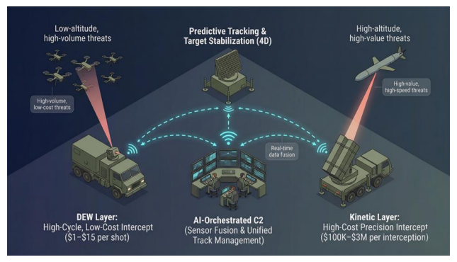
Figure 1. Emerging multi-layered defence architectures integrating kinetic and directed energy systems through AI-driven command and control.
The Problem: Capability Without ControlThis advantage, however, is not absolute. Real-world deployments continue to reveal persistent constraints—thermal limits, atmospheric attenuation, beam dwell time, and power scalability challenges. These are not isolated engineering challenges; they are systemic constraints.
More importantly, they reveal a deeper dependency: the effectiveness of directed energy systems is inseparable from the ecosystem that supports them. Performance is not defined solely by the platform, but by the electronics, semiconductors, and supply chains beneath it.
This creates a structural risk. A nation may deploy advanced directed energy systems, yet remain dependent on external control at the component and semiconductor level.
The future of defence, therefore, will not be determined by the deployment of advanced platforms alone, but by the ability to secure control over the enabling ecosystem that makes those platforms viable at scale.
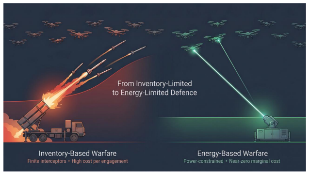
Figure 2. Directed energy systems deliver visible capability, but remain dependent on underlying electronics and semiconductor ecosystems—creating hidden vulnerabilities in control.
The Economic War of AttritionAt the heart of this transformation lies a fundamental imbalance shaping modern conflict. Defenders are increasingly forced to deploy high-value interceptors against low-cost threats, creating an unsustainable economic equation. Systems such as surface-to-air missiles or kinetic interceptors become prohibitively expensive when faced with saturation attacks.
This imbalance is not incidental—it is being deliberately operationalized through drone swarm attacks and loitering munitions designed to overwhelm defences through sheer volume rather than technological sophistication. The objective is clear: to stretch defensive resources to their limits and exploit the cost asymmetry inherent in traditional systems.
Directed energy systems fundamentally alter this equation. By shifting from consumable munitions to energy-based engagement, they dramatically reduce marginal costs and enable sustained operation without the constraints of inventory—as long as sufficient power is available.
This represents more than a technological evolution. It is a financial reset in how defence is structured and sustained. This is the defining shift from inventory-based warfare to energy-based warfare.
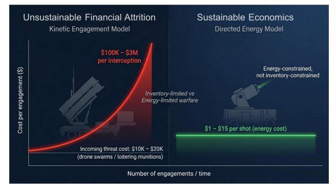
Figure 3. Cost asymmetry in modern warfare—low-cost threats forcing disproportionately expensive kinetic responses, driving unsustainable defence economics.
Without such a transition, the long-term economics of defence operations risk becoming untenable in the face of increasingly scalable, low-cost threats.
The Illusion of SovereigntyThe visible success of a directed energy intercept can be compelling. It signals speed, precision, and technological sophistication—creating the impression of true strategic independence. But that impression can be deceptive.
Beneath every such system lies a tightly integrated ecosystem of power electronics, thermal systems, optical assemblies, RF components, and semiconductors. If these critical elements are externally sourced, control has not been achieved—it has merely shifted out of view. Dependence is not eliminated; it is reconfigured.
In practice, this dependence surfaces through export controls, defence supply chain choke points, firmware constraints, and restricted access to advanced semiconductor nodes. Under normal conditions, these limitations may remain hidden. Under geopolitical stress, they translate directly into operational risk.
Capability alone does not ensure sovereignty.
Control does.
Where Control Actually ResidesTo understand where control truly resides, directed energy systems must be viewed not as standalone platforms, but as layered architectures.
At the surface lies the platform layer—the visible capability, including laser systems deployed on land, sea, or air platforms. Beneath this sits the system layer, where command-and-control frameworks, targeting systems, and sensor fusion enable coordinated operation.
Deeper still is the engineering layer, which determines real-world performance. This includes power electronics that stabilize output, thermal systems that govern endurance, and optical and beam control mechanisms that ensure precision.
At the foundation lies the control layer—the least visible, yet most decisive. This layer encompasses semiconductors, advanced materials, packaging, and the broader supply chain that sustains the system.
It is this lowest layer that anchors performance, scalability, and resilience. Any external dependence here propagates upward, constraining every layer above and limiting true autonomy.
Performance, scalability, and resilience are determined at the lowest layer. Any external dependence at the control layer propagates upward, constraining the entire system.
Sovereignty, in this context, is not a function of the platform—it is a function of control at the component and semiconductor level.
These constraints are not theoretical—they are engineered into the system itself.
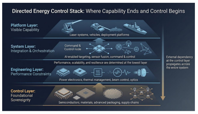
Figure 4. Directed energy performance is constrained by tightly coupled power, thermal, and semiconductor systems—highlighting the central role of control-layer technologies such as GaN-based switching.
The Real BottlenecksThe challenges facing directed energy systems are physical, not conceptual.
- Thermal constraints limit sustained firing duration
- Advanced power electronics define efficiency
- Atmospheric conditions degrade beam propagation
- Beam dwell time limits effectiveness against fast-moving targets
- AI-enabled defence systems must operate at machine speed
Figure 5. Directed energy constraints are interdependent—thermal, power, and control limitations must be solved as an integrated system, not in isolation.
These constraints do not exist in isolation—they reinforce and amplify one another. Addressing a single limitation, whether in thermal management or power delivery, does not translate into real operational capability on its own. What is required is coordinated industrial depth across multiple domains, from materials science and semiconductor design to power systems and real-time computation.
A directed energy system is only as effective as the ecosystem that sustains it.
From Weapons to SystemsDirected energy is no longer a standalone capability. It is steadily becoming part of integrated, AI-orchestrated defence architectures—often described as Cognitive Hybrid Defence—where multiple systems operate in coordination rather than isolation. In this emerging model, directed energy systems function alongside electronic warfare, cyber capabilities, and kinetic interceptors, all unified through real-time command-and-control frameworks.
Figure 6. Transition from standalone weapons to AI-orchestrated, multi-layer defence systems, where threats are dynamically assigned to the most efficient response layer.
This shift is already visible in operational programs such as the U.S. Navy’s HELIOS system and Israel’s Iron Beam, both of which demonstrate how layered, multi-domain defence is replacing single-point solutions. The objective is no longer limited to individual interception—it is about orchestrating responses across domains with speed, precision, and economic efficiency. As this transition accelerates, control over the underlying technological ecosystem becomes even more critical.
Semiconductor Policy is Defense PolicyThis convergence carries direct implications for national strategy. Defence capability and semiconductor capability can no longer be treated as separate domains—they are structurally interdependent. Initiatives such as India’s Electronics Component Manufacturing Scheme (ECMS) and the India Semiconductor Mission (ISM 2.0) must be viewed through this lens. These initiatives are central to building semiconductor sovereignty and securing India’s position in the global defence technology supply chain. They are not merely industrial policies; they are foundational to future defence capability.
Yet the challenge is not one of intent or conceptual understanding. It lies in industrial depth—particularly in manufacturing, materials ecosystems, and advanced semiconductor fabrication. Without control over critical technologies such as Gallium Nitride (GaN)-based power electronics systems, advanced packaging, and high-reliability electronics, there is a real risk of remaining a system integrator rather than a true control holder. Sovereignty, in this context, is not achieved through system assembly but through ownership of the components and technologies that define performance and resilience.
Figure 7. Defence capability is fundamentally anchored in semiconductor ecosystems—spanning materials, manufacturing, and advanced power electronics such as GaN-based systems.
Conclusion: Capability vs ControlWhat emerges is a broader shift in how warfare itself is understood. We are moving into a phase defined by energy, integration, and system-level thinking. Directed energy systems will become increasingly visible on the battlefield, delivering immediate and measurable impact. However, the true determinants of success will remain largely invisible—embedded in defence supply chains, semiconductor ecosystems, and industrial capability.
This creates a clear strategic imperative. Nations must move beyond assembling advanced platforms to controlling them end-to-end.
Forward OutlookLooking ahead, the defining question of the next decade will not be who deploys directed energy systems first, but who can sustain and scale them under real-world conditions. Future conflicts may become power-limited rather than ammunition-limited, where grid resilience, energy density, and power electronics infrastructure and power distribution emerge as core defence parameters.
Meeting this challenge will require closer alignment between defence procurement and semiconductor strategy, sustained investment in power electronics, thermal systems, and advanced materials, and a decisive shift from platform-centric thinking to ecosystem-centric design.
Countries that recognize this transition early will build not just capability, but resilience. Those that do not will remain dependent—regardless of how advanced their visible systems may appear.
Figure 8. Future defence systems will be constrained by power, energy infrastructure, and semiconductor capability—marking the shift from ammunition-limited to energy-limited warfare.
Final PerspectiveIn the next generation of warfare, capability will be visible. Control will be decisive.
The post Directed Energy Systems: Where Capability Ends and Control Begins appeared first on ELE Times.
Гурток ІПСАК «Інженерія та програмування систем» на ФІОТ

На Факультеті інформатики та обчислювальної техніки (ФІОТ) КПІ ім. Ігоря Сікорського запрацював гурток ІПСАК «Інженерія та програмування систем (на базі автономних комплексів)».
Vector Photonics demos free-space optical communication using PCSEL outside of a lab
Новий студентський простір у ВПІ

У Навчально-науковому видавничо-поліграфічному інституті (НН ВПІ) КПІ ім. Ігоря Сікорського презентували оновлене укриття та новий студентський простір.
CSconnected extends deadline for fourth funding round of supply chain development program
Supra extends pre-seed funding round with Rio Tinto as strategic investor
My new Workbench and Setup!
 | Hi everyone! I just finished my new workbench! I extended my existing one(the one facing the desk behind) with the edge-piece facing the wall. Also I sanded the desk surfaces and gave them a new finish. And last but not least, I added the shelf above for all devices. As you can see it is not completely finished, I am still working on the LED strip that goes below the shelf and some other refinements. But so far I am very pleased with the results! [link] [comments] |
Сторінки

