


Збирач потоків
Weekly discussion, complaint, and rant thread
Open to anything, including discussions, complaints, and rants.
Sub rules do not apply, so don't bother reporting incivility, off-topic, or spam.
Reddit-wide rules do apply.
To see the newest posts, sort the comments by "new" (instead of "best" or "top").
[link] [comments]
Radxa Linkr: A Pocket-Sized IP KVM for Browser-Based Remote Control
Radxa Linkr is a compact IP KVM that turns a computer into a machine you can control remotely, from anywhere. The device, about the size of a USB stick, connects to the target PC via HDMI for video and USB for keyboard and mouse. From then on, access happens through a web browser, with no need to install dedicated apps. You can manage the system even when it is off or during boot, for example to change BIOS settings.
Communication with the user happens over USB-C, Ethernet, or WiFi 6, in both client and access point modes. This means you can reach the device from a local network or from the internet, perhaps through a VPN. In addition, built-in support for Tailscale VPN and two-factor authentication makes the connection more secure. Everything is managed by a web interface that works on any operating system.
Hardware and components of Radxa LinkrThe heart of the device is the Rockchip RV1106G3 SoC, which integrates an Arm Cortex A7 CPU at 1.2GHz with a RISC-V co-processor. The 1 TOPS NPU handles AI processing, while the third-generation 5MP ISP and VPU support H.265/H.264 encoding up to 3072×1728 (5MP) at 30fps. System memory is 256MB DDR3L on-chip, with optional storage via a 16GB eMMC flash.
For video capture, the board uses an HDMI-to-MIPI CSI bridge (Rockchip RK682F) that supports inputs up to 2K at 30Hz. Connectivity is handled by a WiFi 6 module (AIC8800) and a RealTek RTL8152B Ethernet port. Power is 5V/2A via the USB-C port, and overall dimensions are just 70 x 22 x 12 mm. The price starts at $59 on AliExpress, Amazon, Arace, and Allnet.
The project page on the maker’s site documents the technical specifications and usage modes. In addition, the system supports advanced features such as integration with AI agents like OpenClaw and Hermes, which can automate diagnostic or maintenance operations on the remote computer.
Operation and browser accessAccess to Radxa Linkr happens through a web browser, with no dedicated software needed. Once the device is connected to the network, you open its web interface and configure the connection to the target computer. The interface shows real-time video and lets you use keyboard and mouse as if you were in front of the machine. You can also change the video resolution and manage multiple devices from a single panel.
The device also works before the operating system boots, so you can access the BIOS or bootloader. In addition, WiFi access point mode lets you connect directly to Linkr when no network is available. For those who need a stable connection, the Ethernet port offers a valid alternative to WiFi. Finally, the USB-C port can be used for power or for a direct connection to a PC.
 Radxa Link web interface
Power management is efficient thanks to the low-power SoC, but it is important to power Linkr with a 5V/2A adapter to ensure stability. As for cables, a good-quality HDMI cable is essential to avoid video interference. Also, if you want to extend the distance between Linkr and the computer, you can use a longer HDMI cable, but it is advisable to keep the USB connection short to avoid power issues.
A 5-meter HDMI 2.1 cable can be useful for placing the device in a convenient spot while maintaining video quality. However, for the USB port it is better to use a short, shielded cable. In addition, for those who want to expand logging capabilities, a MicroSD Card Reader module with SPI interface can be connected to save diagnostic data or video recordings.
Software and advanced featuresRadxa Linkr’s firmware is designed to be simple yet powerful. The web interface includes a management console that lets you configure the network, update the firmware, and manage users. In addition, Tailscale VPN integration simplifies secure remote connection, while two-factor authentication adds a layer of protection. For more advanced users, AI agents like OpenClaw and Hermes can be enabled to automate repetitive tasks.
The list of main features includes:
- Full remote access via browser, even before system boot
- WiFi 6 support in client and access point modes
- 10/100 Mbps Ethernet port via USB-C adapter
- Integrated Tailscale VPN and two-factor authentication
- Integration with AI agents like OpenClaw and Hermes
- H.265/H.264 video encoding up to 5MP at 30fps
In conclusion, Radxa Linkr is a versatile tool for anyone who needs to access their computers remotely, whether for work or personal use. Its compactness and advanced features make it an interesting choice for makers who want to experiment with remote control. With a starting price of $59, it is an accessible investment for those looking for a modern KVM over IP solution.
Source: https://linkr.now/
The post Radxa Linkr: A Pocket-Sized IP KVM for Browser-Based Remote Control appeared first on Open Electronics.
Testing a new CAN chip (TCAN3414DR), scope probes soldered directly to the pins
 | submitted by /u/m4rkw [link] [comments] |
Panasonic at Electronica: Next-gen Solutions for Industrial, Automotive, Telecom, and AI Applications on Display
Panasonic Industry seems to be driving innovation through consulting, designing, and supplying a wide range of technologies and systems to various industries. These include automotive, e-mobility, telecom, factory automation, infrastructure, manufacturing & logistics, and HVAC. the company participated in Electronica 2026 at Bengaluru and showcased its comprehensive portfolio of advanced technology Components and Solutions at the expo. The company has designed these solutions for diverse applications across Industrial, Automotive, Railways, Telecom, and Digital Infrastructure (Data Center) sectors during the Electronica India 2026, one of the world’s largest electronics expo held in Bengaluru.
A Wide Display of Cutting-edge TechnologyAt the exhibition, Panasonic introduced new technology of Fine Conductive Material, and EDLC (Electric Double Layer Capacitor), BLDC Motor, DC Pump and Polymer Capacitors for Data Center applications, along with the Electro-mechanical & Passive Components for Automotive (ADAS, EV ecosystem) and Industrial (smart meters, railways, automation) use cases, PCB Laminate Materials for high-frequency PCB solutions. These solutions have been designed to cater to India’s evolving Industrial and Automotive segments, significantly contributing towards enhancing performance, safety and reliability.
While inaugurating the Panasonic Industry stall at the Electronica India 2026, Hirokazu Kamoda, DMD, Panasonic Life Solutions India, said, “India’s electronics industry is entering a phase of accelerated transformation, with rapid growth across automotive, industrial, and digital infrastructure segments. At Panasonic, we are committed to enabling this transformation by bringing-in advanced, reliable, and sustainable component solutions rooted in Japanese innovation and tailored to meet Make-in-India vision. We are also implementing Digital initiatives to strengthen and expand our reach to the widespread customers across India, and create Digital Sales Platform to fulfil their requirements seamlessly with speed”.
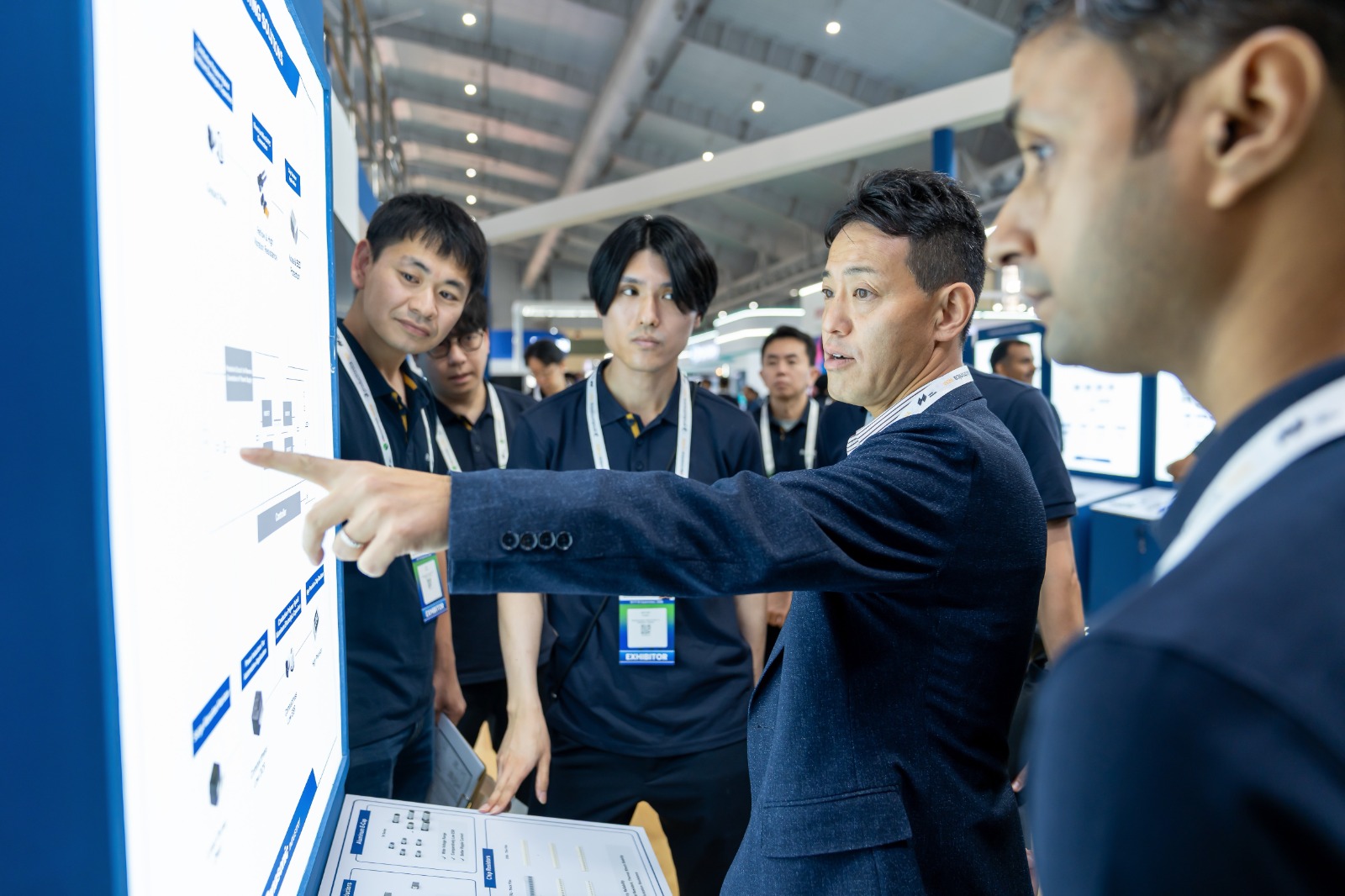
Naoki Nakazono, Managing Director, Global Sales Division, Panasonic Industry Co. Ltd., added, “Panasonic Industry has been supporting global innovation for over a century, and India is an increasingly important part of this journey. Through our participation at Electronica, we aim to showcase innovations and technologies that empower OEMs to drive efficiency, safety, and intelligence in applications ranging from AI and telecom to automotive and digital infrastructure.”
Further, Narayan Kumar, Chief Business Office, Panasonic Industry & Energy India (PIDEIN), Panasonic Life Solutions India (PLSIND), said, “We work very closely with our customers in India, who are looking for solutions that not only deliver performance but also ensure long-term reliability and cost efficiency. Whether it’s Polymer Capacitors for AI servers, high-frequency PCB laminate materials, or our new Fine Conductive Materials, every solution reflects our commitment to elevating their (customer/OEMs) manufacturing capabilities, which in turn advances industrial proficiency within the ecosystem in our country.”
The post Panasonic at Electronica: Next-gen Solutions for Industrial, Automotive, Telecom, and AI Applications on Display appeared first on ELE Times.
Tip: "no-clean" solder paste - clean it!
 | "no-clean" solder paste leaves really messy looking residues having fine pitch connectors (looks like a cracked salt deposition). The pictures show the before and after cleaning using an ultrasonic bath and flux remover agent (bath ph = 12, 50 °C, 5 min). Cleaning with isopropanol and flux-off using brushes did not work at all (hard to find a suitable brush, hair size vs hair hardness). Conclusion: Always clean your boards for best results. Connector pad specs: - 400 um pitch - 200 um pad width - 100 um mask dam (sliver) - 50 um mask expansion [link] [comments] |
Lumina Desk: The Restaurant Table That Takes Orders by Voice
Lumina Desk is a restaurant table that takes voice orders, without apps, QR menus, or waiters. A Raspberry Pi with microphone, speaker, and ePaper screen manages the entire cycle: the guest speaks, the system transcribes, interprets, shows the order on the display, communicates it to the kitchen, and collects payment via UPI QR. The project is by Shubhjaiswal408, and Shubhjaiswal408’s repository contains all the code to rebuild it.
The heart of the system is wake-word detection for ‘Hey Lumina’, handled by the on-device openWakeWord model. Once woken, the microphone captures the guest’s voice and transcribes it with Groq Whisper (whisper-large-v3-turbo) if there’s a connection, or with Vosk in offline mode. The text is then passed to an LLM, GPT-OSS-20B online or LFM2-700M offline, which interprets the intent. However, prices, wait times, and allergens are never left to the model: they are calculated in Python from the restaurant’s real menu.
For the most common requests, like ordering a pizza, asking for the bill, or checking an allergen, the system doesn’t even go through the LLM. A rule parser classifies them in under 5 ms, making the experience almost instantaneous. Additionally, the menu of the Auntyno-Z Pizza restaurant in Ghodasar includes 189 dishes, of which 66 are pizzas, and the parser handles them all without a hitch.
The data flow: from voice to order in the kitchenOnce the request is interpreted, the order state is published to an MQTT bus. Two services subscribe to this bus: the first generates an 800×480 pixel image and sends it to the ePaper panel on the table, so the guest sees the summary in real time. The second is the kitchen dashboard, which receives the order ready for preparation. This approach separates recognition logic from display, making the system modular and easy to extend.
Payment happens via a dynamic UPI QR code showing the exact bill amount. Payment confirmation is read directly from the merchant’s emails via IMAP, so the system knows when the order has been settled and can reset the table for the next customer. Everything runs on a single Raspberry Pi, which also handles confirmation audio through the speaker.
 The system runs entirely on a Raspberry Pi and keeps working without internet. (photo: Shubhjaiswal408)
The project aims to work even without an internet connection, an important choice for a noisy environment like a dining room. In offline mode, transcription uses Vosk and interpretation relies on the LFM2-700M model via Ollama. This 700M-parameter model runs on the Raspberry Pi’s CPU and takes about 9 seconds for processing. That’s an acceptable time for an order, but it shows the trade-off between accuracy and speed when working without the cloud.
To reduce wait times, the rule parser intercepts most phrases. For example, if the guest says ‘I’d like a margherita’, the parser recognizes the pizza, calculates the price from the menu, and publishes the order to MQTT without ever calling the LLM. This way, the system feels responsive in daily use and reserves the 9 seconds of computation only for more complex questions.
For voice synthesis of confirmations, the system uses Piper, a lightweight text-to-speech engine. Finally, image generation for the ePaper screen is handled by the Pillow library, which composes the order summary with high readability. Everything is orchestrated by Python scripts that communicate via MQTT, keeping the code clean and adaptable to other restaurants.
Anyone wanting to replicate the project will find in Shubhjaiswal408’s repository the code for speech recognition, menu management, and MQTT integration. The system was designed for a real restaurant with 189 dishes, so it’s not a demo: it’s a device that has faced noise, different languages, and the need for reliability. For hardware, the Raspberry Pi 5 with 2 GB is an adequate base, although the original project uses an earlier model. The 2 W speaker is sufficient for the short voice confirmations at the table.
Source: https://github.com/Shubhjaiswal408/lumina-desk-smart-restaurant
Related productsThe post Lumina Desk: The Restaurant Table That Takes Orders by Voice appeared first on Open Electronics.
Odisha Gears Up to Become a Force Worth Reckoning in India’s Semiconductor Growth Strategy
The state of Odisha has made its ambition clear: it intends to emerge as a leading semiconductor and electronics hub in the country. In a recent announcement from CM Mohan Charan Majhi at SEMICON India 2026, Odisha announced the development of an 870-acre Odisha Silicon Valley in Naraj, near Cuttack, which will host major Electronics & IT projects. This commitment comes alongside investment proposals worth approximately Rs 23,600 crore, with the potential to generate around 6,100 employment opportunities across the semiconductor and electronics ecosystem.
The CM led a series of high-level engagements with semiconductor and technology companies. The state is augmenting its growing investment pipeline to attract the next wave of investments across the semiconductor value chain. The engagements also saw the signing of a Letter of Intent (LoI) with QuadQuantum for a semiconductor facility to produce SiC Substrate wafers, further strengthening Odisha’s engagement with the semiconductor and technology ecosystem at SEMICON India 2026.
Why was Naraj Selected for Odisha’s Semiconductor Push?The area for Odisha Silicon Valley in Naraj offers a highly favourable strategic location regarding connectivity and industrial infrastructure. With seamless connectivity to the Cuttack–Bhubaneswar urban corridor, the site also provides efficient multimodal access to major ports such as Paradip and Dhamra, along with connectivity to key national highways. These advantages position Naraj as a potential strategic hub for the semiconductor supply chain, logistics and allied industries.
Semiconductor fabrication facilities and assembly units require reliable access to substantial quantities of water and power and the site’s proximity to the Mahanadi River provides a significant locational advantage for meeting industrial water requirements. Combined with its connectivity and infrastructure potential, Naraj offers a strong foundation for developing a world-class semiconductor and electronics ecosystem.
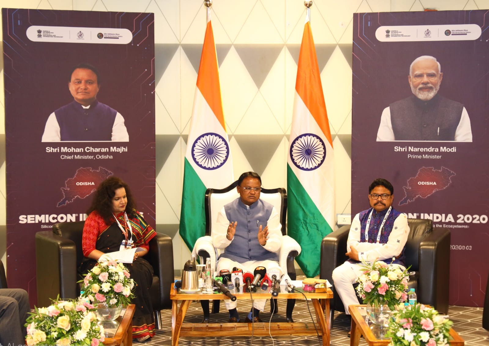
The engagements come as Odisha showcases the progress of its semiconductor journey at SEMICON India 2026. The Odisha Pavilion showcased projects from RIR Power, SiCSem, 3DGS, ARF Design and educational institutions designing the first batch of Made in India chips such as NIT Rourkela and PMEC Brahmapur.
From Sand to Silicon: Establishing the Semiconductor EcosystemOdisha’s journey towards building a semiconductor ecosystem is also being brought alive at the Odisha Pavilion through “Sand to Silicon”. The installation gives a distinctive Odisha expression to the state’s semiconductor journey, connecting its identity with its growing ambitions in silicon and advanced technology. It also ties into Odisha’s larger vision of moving from a “Mine Economy” to a “Mind Economy.”
Beyond the projects already underway, Odisha has been taking measures to build the wider ecosystem required to emerge as a leading semiconductor hub. The state has been among the early movers in aligning its Semiconductor Policy with the evolving India Semiconductor Mission 2.0. Its recent Third Policy Amendment further expanding support to critical parts of the semiconductor value chain.
Through the amendment, Odisha has extended 25% additional fiscal support to ISM-approved projects in semiconductor equipment manufacturing, semiconductor-grade gases, raw materials and supply-chain segments. The current policy framework also provides support for engineer relocation, manpower skilling, internships, international patents and R&D.
The post Odisha Gears Up to Become a Force Worth Reckoning in India’s Semiconductor Growth Strategy appeared first on ELE Times.
EEVblog 1774 - PayPal Here Part 2 - Security Boogaloo
Hello! I'm a beginner in electronics, and I've built a half-adder using 2N2222A.
 | submitted by /u/timofey2585 [link] [comments] |
CSconnected celebrates impact of Strength in Places Fund program
NewPhotonics and Tower begin high-volume shipments of laser-integrated, serviceable optical engine PICs for scale-out and scale-up AI interconnect
Tower highlighing high-volume silicon photonics and SiGe solutions at ECOC
onsemi unveils Embedded Power Platform
Mactini: the minimalist laptop built on an RP2350
The Mactini turns a satirical BBC meme into a real, working laptop. Tucker Osman built an ultra-small device with a single button that handles every function. The project shows how you can build a minimalist computer with modern components and salvaged materials. The technical documentation is complete, and the result is surprising in both size and engineering.
At the heart of the system is a small Waveshare board based on the RP2350. This board handles the display, audio, and input. The display is a 1.69-inch SPI LCD with an ST7789V2 controller. The resolution is enough for a basic text and graphics interface. Everything is housed in a 3D-printed case designed in FreeCAD.
Firmware and video handling with DMAThe firmware uses DMA to copy screen data, freeing up CPU cycles for other tasks. Video playback is handled through Motion JPEG decoding. This approach lets the device show animations and clips on the small display without overloading the processor. DMA also reduces latency and improves image smoothness.
Audio is handled by an iPad speaker and an amplifier salvaged from a scrap board. This recycling choice lowers costs and shows that parts from broken devices can be reused. The sound is clear, considering the size of the device. The mix of salvaged and modern components makes the project accessible.
3D-printed case and materialsThe case is 3D-printed and designed in FreeCAD. This open-source software lets you modify the design to suit your needs. The shell is compact and protects the internal components. 3D printing also lets you customize colors and finishes. The original project includes the files needed for printing.
To rebuild the project you need only a few key components: the Waveshare board with RP2350, the ST7789V2 display, and a salvaged speaker and amplifier. The full list is available in the documentation. In particular, anyone who wants to replicate the Mactini also needs a 3D printer and filament. The rest is soldering and patience.
The project is documented in detail. The project page on Hackaday.io collects photos, schematics, and a description of how it works. Tucker Osman also shared design choices and the difficulties he ran into. Anyone who wants to dig deeper can check that page to better understand each step. It is a valuable resource for anyone who wants to build their own Mactini.
The Mactini is an example of how a satirical idea can become a concrete object. The combination of a single button, a tiny display, and salvaged audio makes it unique. It also shows that you don’t need expensive parts to build a working computer. It is a perfect project for anyone who loves technical challenges and creative reuse.
Source: https://hackaday.io/contests
The post Mactini: the minimalist laptop built on an RP2350 appeared first on Open Electronics.
A Raspberry Pi Camera Mounted on a Hat
A wearable video camera can be built with a Raspberry Pi 5 and a camera module, all enclosed in a case that attaches to a hat. The project was created to record video while moving without holding anything in your hands. The board runs the Broadcom BCM2712 quad-core processor at 2.4 GHz with Arm Cortex-A76 architecture, and the 2 GB RAM version is sufficient to handle the video stream.
The assembly is shown in the reference video. The source shows how to connect the camera module to the board and how to arrange everything inside the case. Anyone following the video will find the main steps without having to look elsewhere.
The board and the camera moduleThe Raspberry Pi 5 is the fifth generation from the Raspberry Pi Foundation. The 2 GB RAM version uses the Broadcom BCM2712 processor, a quad-core 2.4 GHz chip with Arm Cortex-A76 architecture. This configuration handles the camera module without any issues, and the module connects directly to the board.
The camera module goes into a black plastic case designed specifically for it. The case can sit on a flat surface or be attached with Velcro. The second option is the one needed for the hat: the Velcro keeps everything steady even when walking or running.
The case and the attachmentThe Raspberry Pi Camera Module case is a piece of black plastic that protects the lens and the circuit. Its shape is designed to be compact and comfortable on a hat. The Velcro included in the package lets you attach and detach it in seconds.
Only a few tools are needed for the assembly. The Velcro is cut to the right size and applied both to the case and to the hat fabric. Then the camera module is inserted into the case and the flat ribbon cable is connected to the board’s port.
The result is a lightweight camera that is not intrusive. You can use it for hikes, to document work, or to record a driving session. Video quality depends on the camera module and the light, but the board is never the bottleneck.
- Raspberry Pi 5 with 2 GB RAM
- Raspberry Pi Camera Module
- Black plastic case for the camera module
- Velcro for attachment
- Hat or flat surface
The list above summarizes the essential components. The Raspberry Pi 5 and the camera module are the two main pieces. The case and the Velcro complete the system and make it wearable.
The project also adapts to other uses. The same case with Velcro can be attached to a backpack, a bicycle, or a helmet. The board stays the same; only the mounting surface changes.
For those who want to go deeper, the reference video shows the assembly step by step. The source is especially useful for anyone who has never worked with a Raspberry Pi and needs to see the connections live.
Source: https://youtu.be/Hn-ClS2fmMU?si=BrOk84blJevP5YHU
The post A Raspberry Pi Camera Mounted on a Hat appeared first on Open Electronics.
FPGA architecture: SEU detection and recovery strategies

Part 1 of this mini-series covering single event upset (SEU) challenges in FPGA architectures examined radiation particles and related SEU challenges for FPGA applications that require robustness and predictability in ground-based and terrestrial applications.
Part 2 of the mini-series will cover SEU detection, recovery, and validation for FPGAs used in mission-critical systems such as aerospace, defense, telecommunications, and industrial applications.
Detection and recovery from SEUs require a layered strategy that addresses the distinct vulnerabilities of configuration RAM (CRAM), user logic, and embedded data storage. No single technique provides comprehensive coverage across all FPGA resource types. Instead, an effective approach combines complementary methods, each targeting a specific failure mode, with recovery mechanisms that are tightly coupled to the detection events that trigger them.
The following sections describe the detection techniques and their associated recovery strategies, from configuration-layer monitoring to logic-level redundancy to system-level behavioral observation.
CRAM readback and scrubbing
CRAM readback is the most basic detection technique for SEUs in CRAM. The system calculates a cyclic redundancy check (CRC) for the bitstream. An internal hardened configuration block in the FPGA reads back the CRAM contents and compares the calculated CRC to the expected result. If the results don’t match, the system can set a status flag to alert the user, for example via an internal interrupt to a soft processor or an external pin to a system-level board controller.
If the system flags an SEU error, the user can take action, for example:
- Stop the FPGA application and reload the bitstream, overwriting the CRAM to fix the flipped bit.
- Wait for an accumulation of SEUs before halting the application and reloading the bitstream.
- In some applications, it may be acceptable to power cycle the board and thereby the FPGA, which automatically reloads the bitstream upon power-up.
SEU scrubbing is another SEU recovery technique. Some FPGAs contain blind scrubbing circuits that run in the background and can periodically rewrite the entire bitstream regardless of whether the system detects an error. It’s easy to implement blind scrubbing because it does not require comparison logic; the downside is that blind scrubbing cannot give diagnostics on error rates and specific locations of SEU.
You can schedule scrubbing continuously or for a fixed period, depending on the application and trade-offs on additional power utilization. At terrestrial levels, you can usually set scrubbing intervals further apart, while at higher elevations, given the higher probability of radiation particles, intervals should be shorter.
More advanced SEU readback scrubbing circuits can detect and fix SEUs and report multiple upsets within a bitstream frame. Recent FPGA architectures have bitstreams that have frames that program subsets of the CRAM. Each frame is protected with single error correction and double error detection (SECDED). The SEU readback scrubbing circuit reads the contents of the CRAM and compares the calculated error correction code (ECC) for each frame with a known good ECC for that frame.
If the comparison fails, the circuit can locate the single bit failure based on the ECC mismatch signature and re-write the bitstream frame with the incorrect bit corrected. The SEU readback circuit is more complex and can give better diagnostics for error rates and failure locations. If the readback detects multiple uncorrectable errors however, you may need to reload the entire bitstream or power cycle the FPGA.
Error detection and correction for block RAM
Block RAM upsets require a dedicated detection and correction strategy because the stored data changes dynamically during operation and cannot be protected by static configuration scrubbing. Data written to RAM is wider by a certain number of bits, depending on the data width and encoding used for protection.
If you use an ECC encoder when writing data to RAM, you can use an ECC decoder when reading from RAM to detect corruption. ECC encoders and decoders can detect and correct single- and double-bit errors. From a system design perspective, using ECC to protect block RAM adds latency for encoding and decoding.
Some FPGAs have in-silicon ECC encoders for writing to the RAM and ECC decoders for reading from the RAM to detect and correct corrupted bits. These hardware-based encoders/decoders use more silicon area, have higher power, and have additional output delays. Implementing ECC encoding and decoding in your RTL design is a good option if few block RAMs are used for critical functions such as soft processor program memory, high integrity data paths, or state machine storage.
Triple modular redundancy (TMR)
TMR is the most robust mitigation strategy to guard against SEU errors. TMR requires three independent copies of a circuit to produce the same output. Each circuit has its own copy of combinational and sequential logic. The system compares the result from all three circuits, and two out of the three must match. This method provides a correct result even if one circuit is corrupted.
TMR provides continuous cycle-to-cycle error masking without any detection latency, and is very effective for protecting state machines, control logic, and safety-critical signal paths. However, TMR requires very strict architectural implementation to guarantee that none of the circuits share logic or routing with each other.
Although robust, TMR comes with a large trade-off in terms of FPGA resource usage and power. You need to use at least three times the resources to accommodate the triple redundancy and plan on higher power requirements as a result. Additionally, TMR cannot self-correct a bit error. A bit flip in one of the circuits continues to be corrupt until CRAM scrubbing can address the corruption.
Measuring SEU rates in FPGAs
Quantifying the reliability of an FPGA’s exposure to SEU can be done with specific testing using particle beam accelerators in specialized facilities. The standard figure of merit for terrestrial SEU rate is the soft error rate (SER) expressed in failures in time (FIT), where one FIT equals one failure per 10⁹ device hours.
Most FPGA manufacturers that support SEU detection and scrubbing reserve time at reputable facilities that can provide high energy beams of heavy ions, neutrons, protons, and alpha particles. Facilities can be found in the U.S., Canada, Switzerland, and Japan. This ground-based approach for accelerated testing helps to characterize the FPGA family’s radiation sensitivity. FIT data from the testing helps predict upset rates in target environments.
Ground-based testing and analytical modeling provide pre-deployment FIT rate estimates, but operational monitoring during deployment in the application environment provides the most accurate characterization of device behavior. CRAM detection and scrubbing circuits can log time, location, and frequency of detected SEUs, which you can compare to pre-deployment predictions.
If you observe rates that differ from pre-deployment predictions, you can redesign critical circuits, change scrubbing intervals, and/or change operational range. Most FPGA users work closely with their FPGA vendor to understand measured ground-based FIT rates from beam testing within a specific family and compare it to the application environment testing results.
FPGAs with SEU capabilities
Take the case of Efinix’s Titanium and Topaz families that are built on TSMC’s 16-nm FinFET process. These FPGAs benefit from the inherent SEU sensitivity advantages of the FinFET geometry relative to planar 2D transistor architectures at equivalent geometry.
These FPGas have characterized SEU behavior through independent testing conducted per JEDEC Std. JESD89A for alpha particles and per STd. JESD89 and JESD89-A for neutron particles, providing design engineers with measured FIT data from which you can determine system-level reliability.
The company’s Titanium FPGAs have CRAM SEU detection that lets design engineers monitor configuration integrity and respond to detected upsets through external recovery actions. Efinix also provides data on the FIT contribution from SEU events (transient failure rate) in a soft-error rate (SER) report.
Design engineers can use this data to determine whether on-chip mitigation features are required to achieve target Probabilistic Metric for random Hardware Failures (PMHF) values under ISO 26262-5 for their specific ASIL level.
Next, Titanium Edge FPGAs pair SEU detection capability with hardware scrubbing. The scrubbing architecture implements SECDED on a per-frame basis, operating at clock rates up to 80 MHz. SECDED enables automatic single-bit error correction without an external processor, and it flags uncorrectable double-bit errors for system-level response.
The SEU detection is configurable to meet different application needs. Automatic detection cycles through CRAM frames without user intervention, providing the lowest mean time to detection and the highest assurance of configuration integrity. Manual monitoring allows you to initiate a scrub cycle on demand.
Similarly, you can set detection and correction triggering as automatic, manual, or fixed-rate operation, tailoring the scrubbing interval to your deployment environment’s potential SEU rate. To support design validation and test system robustness, Titanium Edge FPGAs include a hardware error injection capability that can inject a single-bit error at any location within the CRAM array.
Finally, Topaz FPGAs have similar SEU detection capabilities as the Titanium family, but they don’t have the Titanium Edge scrubbing architecture overhead. System designers can monitor detected SEU errors and recover from them via an external action. This family is targeted at high-volume applications such as machine vision, industrial robotics, and broadcast imaging and controls.
Why SEU detection is critical
Radiation-induced SEUs represent a reliability challenge in modern FPGA design and technology. SEUs can silently flip bits that corrupt configuration memory, embedded memory, routing, and logic, thereby negatively impacting system behavior.
The threat to smaller process geometry FPGAs affects terrestrial applications as well as ground-based applications where thousands of FPGAs may be deployed in a system. Ground-based FIT rates may be low for a single FPGA, but when thousands are deployed, the probability of SEU impacting system behavior may increase to a level that requires detection and recovery.
Packaging technology advancements to reduce trace radioactive impurities and alpha particle emission have helped FPGA vendors reduce FIT rates. However, heavy ions, protons, and neutrons continue to expose FPGA vulnerabilities and require heavy beam testing to quantify the sensitivity to SEU and resulting FIT rates.
Detecting SEUs and scrubbing FPGA CRAM are critical to quantify an accumulation of errors that may require a reconfiguration or power cycle. Similarly, quantifying SEU errors within a specific altitude profile can guide systems on scrubbing cycle time by analyzing system power trade-offs versus expected error rates.
You must also analyze the trade-offs when planning for embedded block RAM protection. Error detection and correction require a lot of logic resources that could be soft or hardened in silicon. If you don’t need to detect and correct errors in all block RAM, a soft implementation for mission-critical block RAM can save power and resource utilization.
The most comprehensive strategy to protect against critical control and data path errors is TMR, but with a heavy cost of three times the resources and additional power. Alternatively, some applications may use a mix of TMR, block RAM ECC, and CRAM SEU detection and scrubbing.
No matter which method you choose for mitigating SEU exposure, it’s important to work with the FPGA vendor to understand their testing methodology and resulting FIT rate data. The FPGA FIT rate data can then be extrapolated to understand and compare actual measurements with the application profile.
 Mik Ichiba is principal field applications engineer at Efinix. He is a seasoned semiconductor and embedded systems professional with more than 30 years of experience spanning hardware architecture, PCB design, ASIC development, FPGA architecture, and system-level engineering. Throughout his career, Mik has worked across the hardware design lifecycle, helping organizations translate complex technical requirements into practical, high-performance solutions.
Editor’s Note
This is Part 2 of the mini-series about SEU challenges in FPGA architectures. Part 1 covered SEU radiation particles and related SEU challenges for FPGA applications that require robustness and predictability in ground-based and terrestrial applications.
Related Content
- Using FPGAs in mission-critical systems
- Rethinking the Logic-Routing Tradeoff in FPGAs
- Understanding Single Event Effects (SEEs) in FPGAs
- Enhancing robust SEU mitigation with 28-nm FPGAs
- Learn about SEU Immunity in Terrestrial FPGA Applications
The post FPGA architecture: SEU detection and recovery strategies appeared first on EDN.
Texas Instruments Showcases EV and Sustainable Energy Semiconductor Innovations at electronica India 2026
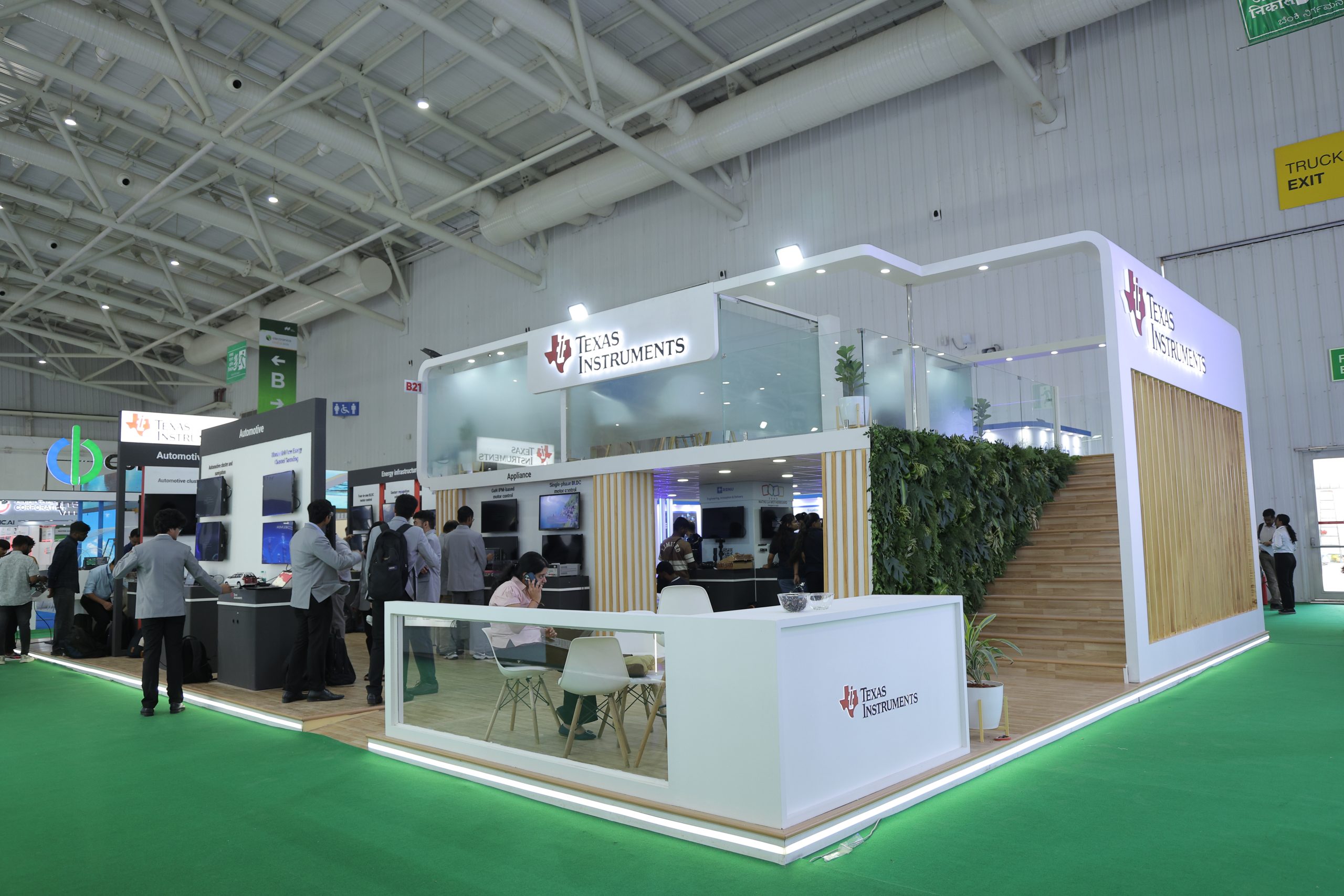
Texas Instruments (TI) is demonstrating more than 20 live demonstrations of its latest analog and embedded processing technologies at electronica India 2026, being held at the Bengaluru International Exhibition Centre (BIEC) from September 16 18. India’s transition toward clean energy is accelerating demand for applications that require high-precision power management, sensing and processing. TI is showcasing how its semiconductor technologies can support greater efficiency and reliability across electric vehicles, industrial applications and sustainable energy systems.
As part of its efforts to strengthen customer engagement in India, TI is enabling customers in the country to purchase products directly from TI, including large-quantity orders. The company says its localized purchasing capabilities provide a more convenient and seamless buying experience. Combined with its technical and design support, the initiative reflects TI’s focus on working closely with Indian customers and helping them move from design to production more efficiently.
“As engineers inventing for engineers, TI focuses on designing and manufacturing semiconductor technologies that help our customers solve increasingly complex challenges,” said Santhosh Kumar, managing director and president, TI India. “We have been part of India’s semiconductor landscape for 40 years, and our commitment here has never been stronger. electronica India 2026 gives us the opportunity to connect directly with the engineers shaping India’s next wave of innovation, building products that are smarter, safer and more energy efficient.”
Semiconductor technologies enable smarter, safer electric mobilityWith India’s adoption of electric mobility accelerating, TI’s semiconductors are enabling engineers to address the growing complexity of electric vehicle architectures, from power management and battery performance to real-time sensing and processing.
- Smarter vehicle architecture: TI is showcasing a 3D car wireframe featuring software-defined vehicle (SDV) central compute, zone control modules, 48V wiper and a Gallium Nitride (GaN)-enabled 48V audio amplifier, along with real-time wheel-speed tracking.
- Commercial vehicle advanced driver assistance systems (ADAS): TI is demonstrating 1V3R (1x camera, 3x radar) solution capable of meeting the technical requirements of ADAS mandates that apply to commercial vehicles in India.
As India scales renewable energy and modernizes its power infrastructure, TI’s semiconductor technologies are driving greater efficiency, reliability and intelligence across applications such as solar inverters, smart-grid infrastructure, motors and appliances.
- Single phase string inverter: TI is demonstrating a GaN-based 3.6kW string inverter with a single microcontroller controlling a H-Bridge bipolar modulated DC/AC inverter and a single string photovoltaic input with maximum power point tracking. The converter is optimized for high frequency operation to minimize total solution cost and size. It achieves>96.5% efficiency at full power. The single-phase string inverter platform is intended to accelerate the development of residential solar power systems.
- Meshed network architecture: TI is showcasing a Wirepas Platform, which is a standard-based connectivity platform built for infrastructure-grade IoT deployments at massive scale. It consists of two components, Wirepas mesh connectivity and the Wirepas Network Management System, and addresses diverse geographies and use cases through a wide range of radio profiles.
TI is continuing to strengthen its commitment to the Indian market by making its products easier to access and buy locally. In addition to buying directly on TI.com in Indian rupees, TI has now expanded INR capabilities to eligible customers in India through their backlog channel. INR billing offers greater cost predictability and flexibility with better delivery terms for its customers in India.
By combining semiconductor technologies with local engineering expertise, technical support and a more convenient purchasing experience, TI is helping Indian customers design and build products for evolving automotive, energy and industrial applications.
TI at electronica India 2026At electronica India 2026, in Hall 5, Booth B21, BIEC, TI will demonstrate how innovation across its analog and embedded processing portfolios is enabling what’s next in electric mobility and sustainable energy, with engineers on-site to discuss how TI’s solutions can address the challenges facing Indian engineers.
The post Texas Instruments Showcases EV and Sustainable Energy Semiconductor Innovations at electronica India 2026 appeared first on ELE Times.
My collection of iron-core transformers that I salvaged from old electronics
 | The 3 transformers on the 1st pic are rated for 220V - 240V While on the 2nd pic are rated for 100V (they're from Japan). [link] [comments] |
Some of my planning sketches for my first projects
 | Diagram of circuit and perfboard arrangement. Mainly posted since a few people stated that my perfboard arrangement was too cramped and "couldn't work" [link] [comments] |
Сторінки




![[link]](https://i.redd.it/gh5anpypzgqh1.png)