


Збирач потоків
Accelerating the shift to next-gen SDVs with zonal MCUs

As the automotive industry shifts toward software-defined vehicles (SDVs), with features and updates delivered via software, vehicle electrical/electronic (E/E) architectures are evolving. These architectures are moving away from traditional flat and domain-based designs, in which separate control units for each function were the norm, to zonal architectures that group vehicle functions based on various criteria, such as physical location, application group, and other functional criteria in zone electronic control units (ECUs).
In a zonal architecture, each zone of a vehicle, such as front, rear, or cabin, has a high-performance controller managing local devices and communicating with other controllers over high-speed networks. This approach is faster to update, easier to scale, less complex, and even cheaper, but it also presents new technical challenges for automakers to overcome. The good news is that innovative microcontroller (MCU) solutions can help tackle those challenges.
Key challenges in the shift to zonal architecturesZonal architectures offer clear benefits of reducing wiring complexity and consolidating compute resources.
However, each zone controller in an SDV must handle a wide range of tasks, from low-level real-time control of sensors and actuators (such as sensing braking pressure, steering angle, or controlling window-lift motors) to high-level data processing tasks (including controlling advanced safety systems or vehicle dynamics or running local AI models to process sensor data). This means the ECUs in a zonal design require compute capabilities that can handle both time-sensitive and compute-intensive workloads concurrently.
Maintaining freedom from interference among functions is a key challenge. Zonal designs consolidate diverse functions, from safety-critical functions such as braking to non-critical functions such as body control on a single ECU with shared compute and communication resources. Without proper safeguards, a fault in one function could disrupt others.
To prevent this, robust isolation mechanisms such as hardware-enforced separation are needed. Ideally, these features should be embedded in the hardware design rather than software implementation to minimize the impact on performance, behavior, or safety.
In-vehicle networks also need rethinking. Modern SDVs generate massive amounts of data from sensors and devices, including cameras, LiDAR, and radar, to support advanced driver-assistance and autonomous-driving features. The vehicle network must ensure that this data is delivered in a predictable and time-sensitive manner.
Traditional in-vehicle networks such as CAN, LIN, and FlexRay struggle to meet these demands at the scale of the modern SDV. Moreover, Ethernet is increasingly used in vehicles for its advantages in performance, reliability, and connectivity options, and at the same time, many legacy devices in the vehicle still use CAN or LIN.
To ensure network performance and avoid communication bottlenecks, next-gen vehicle controllers should include native support for Ethernet and CAN networking on-chip. A well-architected MCU will also enable sufficient control and acceleration features to reduce latency and ensure predictable message delivery, ultimately resulting in deterministic communications at the vehicle level.
 Next-generation automotive MCUs need to adopt improved, low-latency architectures and design philosophies to overcome key challenges in the shift to zonal architectures. (Source: NXP Semiconductors)
Making updates secure, easy, and fast
Next-generation automotive MCUs need to adopt improved, low-latency architectures and design philosophies to overcome key challenges in the shift to zonal architectures. (Source: NXP Semiconductors)
Making updates secure, easy, and fast
A hallmark of SDVs is the ability and the need to receive secure over-the-air (OTA) updates throughout the vehicle’s life. This contrasts with traditional vehicle designs with dozens of ECUs for which updates are complex, time-consuming, and often performed only in service environments.
For an SDV built on a zonal E/E architecture, software updates can be pushed to a selected number of controllers that can be responsible for the software of an entire region of the vehicle, such as the front zone or the rear chassis zone. To support these frequent updates with minimal downtime, embedded nonvolatile memory (eNVM) needs to be upgraded as well to a more versatile option with much faster write speeds and higher endurance.
How modern MCUs lay the foundation for next-gen SDVsNext-generation automotive MCUs need to adopt improved, low-latency architectures and design philosophies to overcome these challenges. Rather than relying on a homogeneous architecture, the implementation of heterogeneous cores optimized by functions is required.
The NXP S32K5 MCU, for example, integrates different kinds of CPU cores complemented by various accelerators for dedicated functions such as AI/ML, signal processing, and network acceleration, enabling designers to assign the right function to the right core. Furthermore, a dedicated low-power engine is available for simple tasks, such as periodic wakeups and sensor monitoring, which can help optimize battery life in electric vehicles.
The integration of multiple functions of mixed criticality warrants robust mechanisms to ensure freedom from interference. The S32K5 lives up to this challenge by implementing features such as XRDC, an in-house NXP IP for isolation and resource allocation in hardware from pin to core.
Moreover, dedicated network accelerators need to be implemented for CAN2CAN (communication between CAN networks) and CAN2ETH (communication between CAN and Ethernet networks) acceleration to ensure deterministic and low-latency architectures.
In addition, integrating an Ethernet switch with fast data-routing capabilities ensures that the latest-generation Ethernet vehicle architectures can achieve latency requirements with minimal CPU load.
With an embedded MRAM as the eNVM, the S32K5 offers write speeds that are 15× faster than conventional eFlash. Write without erase and endurance of 1M write cycles of MRAM helps optimize costs, simplify software development, and minimize downtime for the frequent OTA updates expected in an SDV architecture.
Building the foundation for next-gen SDVsZonal architectures are emerging as a necessity for next-gen vehicles because they align with the needs of SDVs. They concentrate compute, reduce complexity, and enable new, software-driven experiences. With the latest generation of MCUs as the building blocks, automakers now have more tools to develop zonal vehicle architectures to deliver the high performance, reliability, and flexibility required by next-gen vehicles.
The post Accelerating the shift to next-gen SDVs with zonal MCUs appeared first on EDN.
Phantom-powered solid-state linear airflow sensor

Self-heated Darlingtion transistor pair linearly senses airflow using just two wires for both power in and signal out.
Suppose we take a common TO-92 transistor and heat it to a constant temperature differential above ambient. The power input required to keep it there will be determined by its thermal impedance ZT relative to the surrounding air. This suggests it might be handy for air flow measurement. Maybe even moreso if it needed only a simple two-wire connection for both (phantom) power supply from, and signal delivery to, the supporting electronics.
Wow the engineering world with your unique design: Design Ideas Submission Guide
Please see the Related content listings below for a more detailed treatment of the subject. Figure 1 graphs the resulting power vs air speed relationship. Unfortunately, it’s badly bent.

Figure 1 This graph logs power dissipated vs air speed of a TO92 held at a constant 31oC above ambient. Pw = 31/ZT.
Figure 2 shows a practical thermostat circuit to achieve and maintain the delta-T while outputting a signal predictably related to Pw. It utilizes a Darlington sensor transistor pair (Q1 and Q2) to compensate for ambient temperature and convert the resulting nonlinear Pw curve into a linearized airflow readout. Its current mode, phantom-power output is compatible and convenient for the long cable runs often seen in airflow measurement applications.

Figure 2 This circuit implements a phantom-powered Darlington anemometer with a 40-140 mA current mode output. Adjust R10 to calibrate 40 mA (zero fpm), and R11 to calibrate 140 mA (250 fpm). The adjustments interact so some iteration may be necessary. Sorry ‘bout that.
Q1 serves as the self-heated sensor with Q2 providing ambient temperature compensation. Opamp A2 runs a feedback loop that forces a constant Vbe differential between Q1 and Q2. This establishes a constant 31oC temperature differential between Q1 and ambient. It does this (with the help of Darlington current gain) by forcing Q1’s current draw (I) through R3 to drive Q1’s power dissipation (Pw) to follow the Figure 1 curve of heat-vs-air flow.
Okay so far. But how does compensation for Figure 1’s nonlinearity happen? Well, happily the function of Q1’s Pw vs collector current I isn’t linear either. In fact Pw = 5vI – I2R3. That quadratic I2 term is the key. It creates the lovely linearizing curve shown in Figure 3.

Figure 3 This graph logs Q1 power dissipation vs collector current. Pw = 5vI – I2R3.
The 2nd-order curvature of fig. 3 irons out (most of) the bend in Figure 1 and results in a linear 33 to 125 mA current draw over the 0 to 250 fpm flow rate range. Although the match isn’t perfect, when converted to the 40 to 140 mA by opamp A1 and output transistor Q4, the realized output is a calibrated readout of air speed that differs from ideal by less than +/- 5% from 0 to 250 fpm, as shown in Figure 4.

Figure 4 This graph logs anemometer output vs airspeed. FPM = 2.5(Iout – 40mA).
Note that most (~90%) of the output current is actually drawn by inverted regulator U1 as it maintains a constant 5v across the (thirsty) thermal transistors. All that’s left for A2 and Q4 is to conduct several mA of shim current to establish and maintain calibration, which barely gets Q4 warm. U1, however, can be called on to dissipate about three quarters of a watt and thus should be bundled in a TO220 or similar package.
Stephen Woodward‘s relationship with EDN’s DI column goes back quite a long way. Over 200 submissions have been accepted since his first contribution back in 1974. They have included best Design Idea of the year in 1974 and 2001.
Related Content
- Self-heated Darlington transistor pair comprises new air flow sensor
- Linearized portable anemometer with thermostated Darlington pair
- Nonlinearities of Darlington airflow sensor and VFC compensate each other
- Improve thermal airflow sensor PSRR with just two resistors
- A groovy apparatus for calibrating miniature high sensitivity anemometers
The post Phantom-powered solid-state linear airflow sensor appeared first on EDN.
Ather Energy Begins Rollout of Pothole+ Alerts to Gen 2 and Above Scooters
Ather Energy has begun rolling out Pothole+ Alerts to customers with Gen 2 and above scooters, including the Ather 450 Apex, 450X and Rizta Z. The feature alerts riders to potholes, broken road patches, uneven roads and speed breakers ahead while navigating, using road intelligence built from data generated by Ather’s connected scooter fleet.
Announcing the rollout on X, Ather Co-founder and CEO Tarun Mehta said the feature has been nearly nine years in the making. “The challenge was never the idea. It was the data,” Mehta wrote, noting that Ather’s growing connected fleet has now generated the scale of road intelligence needed to make the feature a reality.
Every Ather scooter is equipped with onboard compute and connectivity, enabling the company to build large datasets over time and develop software-driven features for its customers. According to Mehta, Pothole+ Alerts is one of the strongest examples of how Ather is leveraging connected vehicle data to enhance the riding experience.
When using navigation, riders will receive alerts for potholes, broken road sections, uneven surfaces and speed breakers ahead. Notifications are displayed on the scooter dashboard and can also be heard through the scooter, the Ather Halo smart helmet or any compatible Bluetooth headset, allowing riders to stay informed without taking their attention off the road.
The rollout reflects Ather’s continued focus on building connected features powered by real-world riding data. Mehta added that Pothole+ Alerts is just the beginning, with the company planning to build more rider experiences on top of its growing road intelligence dataset.
The post Ather Energy Begins Rollout of Pothole+ Alerts to Gen 2 and Above Scooters appeared first on ELE Times.
Skyworks and Qorvo announce expected leadership team for combined company
I designed a versatle ESC shield for Nucleo boards
 | This project has been born because I have been trying to develop an ESC (hardware and firmware) on my own. While the most challenging part has been the firmware (being myself a hardware guy), the most frustrating part has been not finding a flexible hardware platform to develop upon. On the internet many interesting and well-designed ESC boards can be found, but all have something missing; a small feature, a small detail, I was never fully satisfied. So I designed one: STARDRIVE SHIELD This is a project with the goal of creating a NUCLEO-64 compatible shield to be used as a flexible platform to develop and test ESC firmware, but also for educational purposes. To do so, I included as many features as possible. These features are not mandatory, but they can be implemented (or not) in the firmware (e.g. SPI, I2C, CAN, HALL) or configured through the hardware interface (e.g. overcurrent protection, 6 or 3 PWM). In this way, the STARDRIVE SHIELD grants flexibility to the developer and it is adapt to various needs. I designed it to be compatible with Nucleo-G474 and Nucleo-F446. Compatibility with other boards has to be verified. The STARDRIVE SHIELD is built around the STDRIVE101 gate driver and BSZ099N06LS5 MOSFETs. It presents 3 low sides shunt resistors and 3 relative INA240A2 current sense amplifiers. With STARDRIVE SHIELD you can implement from 6 step to FOC motor control algorithms. Electrical Characteristics
here the github repo: Let me know your opinion! Especially if you spot a mistake or you have any constructive feedback. [link] [comments] |
Navitas’ Q2 revenue grows 22% sequentially as high-power sector rises 50% year-on-year
AI infrastructure is a multi-fab physical realization stack

When people talk about AI hardware, the conversation usually begins with the AI accelerator. That is understandable. GPUs, custom AI accelerators, CPUs, and high-performance compute dies are the most visible symbols of the AI era. They are also where much of the leading-edge semiconductor investment is focused.
Advanced logic nodes, extreme transistor density, high-performance standard-cell libraries, and sophisticated design methodologies are all essential to scaling AI compute. But an AI accelerator alone does not create AI infrastructure.
A modern AI system is not one chip, one fab, one node, or one technology family. It’s a physical system built from many semiconductor ecosystems converging through packaging, substrates, interconnect, power delivery, cooling, reliability engineering, and manufacturing scale. And that distinction matters.
The AI era is not only pushing logic scaling. It’s forcing the semiconductor industry to rethink how different fab outputs—logic, memory, analog, power, compound semiconductor devices, photonics, MEMS, and mature-node control silicon—come together as one physical infrastructure platform. In other words: AI infrastructure is becoming a multi-fab physical realization stack.
This is the missing link in many AI hardware discussions.
The visible part: Leading-edge logic
The most visible part of AI hardware is the leading-edge logic die. This includes GPUs, CPUs, AI accelerators, network processors, and custom compute engines. These devices depend on advanced process technology, dense routing, high-performance transistors, complex power grids, and increasingly sophisticated design automation.
But the logic die is only the center of computation; it’s not the full system. The accelerator may execute the matrix operations, tensor workloads, inference engines, training loops, and dataflow schedules, but its usefulness depends on everything around it.
- How fast data can reach it
- How close memory can be placed
- How efficiently power can be delivered
- How heat can be removed
- How signals can escape the package
- How optical or electrical I/O can scale
- How the package can be manufactured and yielded
- How the system can be tested, qualified, and deployed
This is why AI hardware is no longer just a logic-node conversation. The accelerator is the most visible object, but the infrastructure stack, outlined below, is the real product.
- Memory fabs: HBM becomes part of the compute architecture
AI compute is deeply memory constrained. The value of an accelerator depends not only on peak compute performance, but on how effectively it can access data. This is why memory fabs are central to AI infrastructure.
DRAM, NAND, and especially high-bandwidth memory (HBM) are no longer secondary components in the system. HBM has become part of the AI compute architecture itself. The location, bandwidth, thermal behavior, power profile, and package integration of memory directly affect system-level performance. This changes the role of packaging.
Advanced packaging platforms such as CoWoS, interposers, bridges, and other high-density integration methods are not merely ways to place chips together. They are mechanisms for bringing logic and memory into a physical relationship that conventional board-level integration cannot support.
The memory fab produces the memory device, but the AI system requires memory to be integrated into a bandwidth-dense, thermally stable, mechanically reliable, and yieldable package. That is physical realization.
- Analog and mixed-signal fabs: The hidden interface layer
AI hardware may appear digital from the outside, but every real system depends on analog and mixed-signal functions. Interfaces, clocking, sensors, converters, retimers, voltage regulators, power management ICs, monitoring circuits, and control loops often come from process technologies very different from leading-edge logic.
These functions are not always glamorous, but they are essential. They help manage signal integrity, power sequencing, telemetry, control, protection, timing, and communication between the digital compute die and the rest of the system. This is one reason mature-node and specialty-node capacity remains important.
Not every device in an AI system belongs on the most advanced logic node. Many functions are better implemented on older, more stable, more cost-effective, or more specialized processes. AI infrastructure therefore depends on both leading-edge and non-leading-edge semiconductor manufacturing. The system is advanced because the pieces work together, not because every piece is manufactured on the smallest node.
- Power semiconductor fabs: Energy delivery becomes a scaling limiter
AI systems are power-hungry. As accelerators, memory stacks, switch chips, and rack-level systems scale, power delivery becomes one of the central limits. This pulls power semiconductor fabs directly into the AI infrastructure discussion.
Power conversion, voltage regulation, current delivery, board-level power architecture, rack-level distribution, and data-center energy efficiency are now deeply connected to semiconductor scaling. Technologies such as silicon power devices, GaN, SiC, advanced voltage regulators, and power management ICs all become part of the AI hardware stack.
The challenge is not simply generating more compute. The challenge is delivering usable power to the compute fabric with acceptable loss, noise, heat, and reliability. This is where chiplet and package architecture become tightly coupled to power architecture.
The industry can no longer treat power delivery as a board-level afterthought. For high-current AI systems, power is a physical design problem across die, package, substrate, board, rack, and facility. A compute die may come from a leading-edge logic fab, but the system cannot scale unless the power ecosystem scales with it.
- Compound semiconductor fabs: Efficiency, RF, and high-performance physical interfaces
Compound semiconductor technologies such as GaN, SiC, GaAs, and related material systems are also part of the broader AI infrastructure stack. They are important for high-efficiency power conversion, RF systems, high-frequency communication, and specialized physical interfaces. While they may not sit inside the main AI accelerator, they support the physical infrastructure around advanced compute.
This matters because AI systems are becoming more energy- and communication-limited. As data centers scale, the efficiency of power conversion, the quality of high-speed links, and the ability to move signals across packages, boards, racks, and facilities become increasingly important. Compound semiconductor devices can play a role in those parts of the system.
Again, this reinforces the broader point: AI infrastructure is not a single-fab product. It’s a convergence of many semiconductor technologies.
- Photonics fabs: Data movement becomes optical
AI scaling is also stressing electrical interconnect. As systems grow from single accelerators to multi-chip modules, boards, racks, clusters, and data centers, data movement becomes a dominant challenge. Electrical I/O remains essential, but optical communication is becoming increasingly important for bandwidth, distance, energy efficiency, and system architecture.
This brings photonics fabs into the AI infrastructure stack. Silicon photonics, lasers, modulators, detectors, waveguides, optical transceivers, and eventually co-packaged optics (CPO) all represent a different manufacturing and integration ecosystem from conventional logic.
But photonic devices alone do not solve the problem. They must be connected to ICs, packaged with optical interfaces, aligned to fiber or waveguides, stabilized against temperature and mechanical stress, tested at the package level, and qualified for product deployment.
This is why CPO is not only a photonics problem; it’s a packaging, thermal, mechanical, electrical, optical, manufacturing, and reliability problem. A photonics fab can create the optical device. But AI infrastructure requires the optical path to become a stable product-scale system.
- Mature-node fabs: The infrastructure control layer
Mature-node fabs are often underestimated in AI discussions. But AI infrastructure depends heavily on mature-node silicon for control, sensing, power management, monitoring, security, timing, industrial interfaces, and system management. Many of these functions do not require leading-edge process nodes. On the contrary, they may benefit from mature, robust, and well-characterized process manufacturing technologies.
The AI system may be marketed around the accelerator, but it operates through a large population of supporting devices. Controllers, power management ICs, sensors, retimers, interface chips, baseboard management devices, and other infrastructure ICs help keep the system functional, observable, and controllable.
Without this layer, the accelerator is only a powerful device without a complete operating environment. This is another reason the AI era should not be understood only through leading-edge logic capacity.
Advanced packaging as the convergence platform
If many fab ecosystems create the pieces, advanced packaging becomes one of the main places where those pieces converge. This is why CoWoS, CoWoP, chiplets, CPO, interposers, bridges, substrates, wafer-scale integration, and advanced package-to-board transitions are so important.
They are not just packaging formats; they are also physical convergence platforms. They bring together logic, memory, photonics, power delivery, substrates, interconnect, thermal paths, and mechanical constraints into one manufacturable system.
But that convergence is difficult because each technology arrives with different physical requirements:
- Logic needs dense routing and power delivery
- HBM needs high-bandwidth proximity and thermal control
- Photonics needs optical alignment and temperature stability
- Power devices need current handling and efficiency
- Analog interfaces need noise control and signal integrity
- Substrates need dimensional stability, low loss, and manufacturability
- Cooling systems need physical access to heat sources
- Test flows need visibility into the assembled system
- Reliability flows need confidence across materials and interfaces
This is why advanced packaging is not only “putting chips together.” It’s the physical realization layer of AI infrastructure.
Why “one fab” thinking is no longer enough
Traditional semiconductor conversations often separate the world into categories: logic, memory, analog, power, photonics, packaging, board, system. That separation is useful for organization. But it can hide the real scaling challenge: how AI infrastructure forces these domains to interact.
The logic die affects memory placement. Memory placement affects package size and thermal behavior. Thermal behavior affects power delivery. Power delivery affects substrate design. Substrate design affects signal integrity and manufacturability. Optical I/O affects package architecture. Package architecture affects test access, reliability, and yield.
The outcome is a coupled physical system. A limitation in one layer can become a bottleneck for the entire infrastructure platform. This is why the industry needs to think beyond individual fab outputs and toward a connected realization stack.
From device performance to physical realization
Device performance is still important. Material properties are still important. Transistor density is still important. But they are not sufficient by themselves. A material with excellent properties must still be processed, patterned, bonded, inspected, assembled, tested, and qualified.
A photonic device with strong lab performance must still survive package stress, temperature drift, fiber attach, calibration, and product reliability. A power device with high efficiency must still fit into a board, rack, or package-level power architecture. A high-density substrate must still meet warpage, routing, via, reliability, yield, and cost targets.
An AI accelerator with impressive compute density must still receive data, power, cooling, and system-level integration. This is the central shift: The next era of AI hardware will not be defined only by the best device. It will be defined by the best realized system.
The multi-fab physical realization stack
A more complete way to view AI infrastructure is as a multi-fab stack:
- Logic fabs create the compute engines
- Memory fabs create the bandwidth and capacity layer
- Analog and mixed-signal fabs create interfaces, control, and conversion
- Power semiconductor fabs support efficient energy delivery
- Compound semiconductor fabs enable high-efficiency power and high-frequency functions
- Photonics fabs enable optical data movement
- Mature-node fabs provide control, monitoring, and infrastructure silicon
- Packaging and OSAT flows bring heterogeneous devices into one manufacturable platform
- Substrate and materials ecosystems provide the physical foundation
- Thermal and cooling systems keep the infrastructure operational
- Test, reliability, and yield flows determine whether the system can scale
This is the AI physical realization stack. It’s broader than the accelerator, it’s broader than the package, and it’s broader than the fab.
AI infrastructure is a convergence problem
AI infrastructure is often described through the language of compute performance. But the real system is much larger. It’s a convergence problem across fabs, materials, packages, substrates, optics, power, cooling, manufacturing, test, reliability, and yield.
Leading-edge logic remains essential, but it’s only one layer. The AI accelerator becomes valuable when it’s connected to memory, powered efficiently, cooled effectively, packaged reliably, linked optically or electrically, controlled by supporting silicon, and manufactured at scale.
That’s why the next phase of AI hardware should be understood as a multi-fab physical realization stack.
- Different fabs
- Different materials
- Different devices
- Different process technologies
- One AI infrastructure system
The companies and ecosystems that win will not be those that optimize one layer in isolation. They will be those that connect many semiconductor technologies into reliable, manufacturable, and scalable infrastructure.
And for that, material properties are important, device performance is important, and packaging density is important. But physical realization is what makes them valuable.
Dr. Moh Kolbehdari is senior director of IC/packaging at Socionext US.
Related Content
- True Wafer-Level Packaging
- Wafer Level Chip Size Package (WLCSP) Guidelines
- Intel’s Embarrassment of Riches: Advanced Packaging
- Nvidia, TSMC, and advanced packaging realignment in 2025
- Intel flash move could put wafer-level packages on the map
The post AI infrastructure is a multi-fab physical realization stack appeared first on EDN.
Insides of drawing tablet looks strange
 | submitted by /u/CrudelisDeus [link] [comments] |
Понад 20 тисяч заяв до КПІ!

КПІ ім. Ігоря Сікорського зберігає лідерські позиції серед закладів вищої освіти за кількістю заяв вступників: 3-тє місце в Україні та 1-ше — у Києві
Aehr’s quarterly revenue grows 33% year-on-year to $18.8m
Семінар "Якість без кордонів: інтернаціоналізація та транскордонне забезпечення якості у вищій освіті"

📌 КПІ ім. Ігоря Сікорського представив досвід міжнародних акредитації освітніх програм на міжнародному семінарі «Якість без кордонів: інтернаціоналізація та транскордонне забезпечення якості у вищій освіті».
Why analog anti-tamper security IP is crucial in the PQC era

The global semiconductor industry is transitioning to the post-quantum cryptography (PQC) era. PQC is changing how digital systems defend against potential mathematical attacks. PQC algorithms are designed to protect against hackers who try to recover secret keys by breaking the underlying mathematics. However, physical hardware attacks can bypass mathematically secure algorithms, even if a PQC algorithm is perfectly implemented.
As organizations migrate to PQC, replacing the cryptographic assets being protected—PQC private keys, root keys, firmware signing keys—becomes costly and complex in deployed devices like automotive electronic control units (ECUs) and industrial or defense systems. When a chip processes post-quantum algorithms, it handles significantly larger key sizes and more complex mathematical operations than legacy cryptography.
This extended processing time and high computational intensity widen the vulnerability window, leaving the silicon exposed to physical tampering such as side-channel attacks (SCAs) and fault injection attacks (FIAs).
Mathematically upgrading to PQC only stops a hacker sitting at a quantum computer miles away. It does not stop a hacker from attempting physical attacks. This is where analog anti-tamper security IP comes into play. Analog sensors provide the first layer of defense to secure the silicon itself by detecting tampering techniques used in physical attacks, such as clock, voltage and temperature attacks, as well as electromagnetic and laser fault injection attacks.
Clock, voltage, and temperature attacks
A clock attack occurs when a hacker alters the incoming clock’s frequency or timing on a chip to cause glitches in an effort to interrupt normal operations and extract sensitive information. A clock attack monitor can be implemented to track the frequency and timing of the clock signal. If there is any unusual activity, an alert would be raised and preventive action taken.
A voltage glitch attack takes place when a hacker tries to tamper with the incoming power supply. Generating voltage drops or spikes can cause errors that impact encryption algorithms and bypass security procedures. A voltage glitch detector identifies when there is an unexpected change in voltage and sets off an alarm to reset or shutdown the system to protect against data loss.
A temperature or thermal attack involves a hacker quickly heating or cooling a device to generate timing or supply errors without having access to the clock signal or power supply. A temperature sensor can check for sudden temperature variations and then apply countermeasures if required.
Electromagnetic and laser fault injection attacks
An electromagnetic fault injection (EMFI) attack is when the hacker tampers with a device using an electromagnetic pulse, so no electrical contact or physical connection to the chip’s pins is required. An EMFI sensor can be integrated into the silicon to detect even small changes in the internal magnetic field on the device and respond swiftly to stop an attack from causing damage.
A laser fault injection (LFI) attack occurs when a laser beam is used by a hacker to induce errors to breach security and corrupt data. An LFI sensor is placed on a chip to monitor specific transient characteristics of a malicious laser pulse. If there are any indications of an attack, then the sensor can ensure that secret keys are erased or the device may be forced into lockdown mode.
PQC’s physical side
As PQC becomes more widely adopted, the frequency and complexity of physical hardware attacks are expected to rise. Whilst the latest cryptographic algorithms may resist quantum computers, hackers will continue to exploit physical vulnerabilities because without robust protection these are often easier than breaking the underlying mathematics.
This looks set to drive demand for analog anti-tamper IP that can detect clock, voltage, temperature, EMFI and LFI attacks, trigger responses such as key zeroization or secure reset if required, complement digital root of trust (RoT) solutions, and strengthen compliance with hardware security requirements in sectors such as automotive, industrial, financial and government.
Analog IP solutions offer a continuous line of defense, including clock, voltage, temperature and EMFI sensors, which complement digital RoT systems. As physical attack routes evolve, adding optical and LFI detection to the physical security envelope will become the benchmark for securing next-generation system-on-chips (SoCs).
While PQC addresses the security of cryptographic algorithms, analog anti-tamper IP protects the physical implementation of those algorithms. As organizations invest in PQC, safeguarding the hardware root of trust and stopping physical attacks becomes an even more critical part of a comprehensive security strategy.
Chris Morrison is VP of product marketing at Agile Analog.
Related Content
- Looming Quantum Threat as PQC Market Expands
- Post-quantum cryptography (PQC) knocks on MCU doors
- Post-Quantum Cryptography Incorporated into SoCs via eFPGA
- The need for post-quantum cryptography in the quantum decade
- Test and Measurement Strategies for QKD, PQC and Hybrid Systems
The post Why analog anti-tamper security IP is crucial in the PQC era appeared first on EDN.
Add-on beat frequency oscillator (BFO) for shortwave radio

Expensive shortwave radios include beat frequency oscillators, so why not also add one to an inexpensive radio version?
Broadcast shortwave (SW) radio use may be declining, but there are still lots of interesting signals to listen to between 1.6 and 30 MHz, such as amateur radio (Reference 1), pirate radio stations (Reference 2), aeronautical weather reports (Reference 3) and long-distance aircraft communications (Reference 4). Unfortunately most of these use Single Side Band (SSB) as opposed to the Amplitude Modulation (AM) used by broadcasters, which cannot be received on cheap domestic SW radios.
Wow the engineering world with your unique design: Design Ideas Submission Guide
AM consists of a radio frequency (RF) carrier wave (in red) which is partially modulated by the information – speech or music – (green), as shown in Figure 1a. The time domain signal in Figure 1a can alternatively be viewed in the frequency domain as in Figure 1b, where the carrier is surrounded by two smaller sidebands containing the information. A diode detector can demodulate this signal. In the time domain, the approach can be regarded as rectification with a low pass filter. In the frequency domain, the non-linear action of the diode mixes the carrier with the sidebands, therefore down-converting it back to an audio signal.

Figure 1 This sequence of images shows AM in the time (a) and frequency domains (b), along with SSB in the frequency domain (c).
SSB lacks this carrier, with only one sideband as shown in Figure 1c. To demodulate SSB, an external carrier signal must be added; the resulting signal can then be demodulated with a diode detector like AM. This additional carrier is sometimes referred to as a Carrier Insertion Oscillator (CIO) or Beat Frequency Oscillator (BFO). Expensive SW radios include a BFO, so why not try and add one to a cheap one?
SSB demodulationMany SW radios for SSB published in hobbyist magazines apply a high amplitude BFO signal to the input of the diode detector alongside the intermediate frequency (IF) signal, as shown in Figure 2a. The high BFO amplitude tends to overload any Automatic Gain Control (AGC) loop. Hence, in this type of receiver the AGC loop is disabled and the radio’s dynamic range is alternatively managed by manual RF and/or IF gain control.

Figure 2 These block diagrams show shortwave radios with BFO (a) and low-level BFO injection (b).
Adding a BFO to an existing radio in the way shown in Figure 2a would involve substantial modification to the radio to disable the AGC loop and integrate a manual RF gain control, if not already present. A second disadvantage with this technique is that because the IF signal has a large amplitude at the input of the detector, it can leak into the BFO and modulate it, therefore introducing distortion to the point of making the signal unintelligible.
The Eddystone EB35 radio from the late 1960s (Reference 5) overcame the leakage issue by injecting a low-amplitude BFO signal into the input of the IF amplifier chain. It does however still disable the AGC and instead rely on manual RF gain control.
Proposed here is a method of injecting the BFO at low amplitude into the input of the IF amplifier chain and controlling its level so as to best match the received signal when the existing AGC loop is operational, as shown in Figure 2b. The BFO with level control can be built into an external box with minimum modification, hence is easy to incorporate and then later remove from a valuable vintage radio receiver.
External BFOThe schematic of the BFO is shown in Figure 3. The oscillator is a Hartley type where a tap on transformer T1 provides the feedback. This is generally at 25% of the winding. T1 is a recycled IF transformer from an old transistor radio. Most low-cost radios like those shown in Figure 2 use an IF frequency between 455 and 470 kHz.

Figure 3 In this BFO schematic, VR1 is the pitch and VR2 is the level.
TR1 is a BC548 transistor, which although not known for its high frequency performance has sufficient gain at 455 kHz. The IF transformer includes a capacitor to set its operating frequency. To operate effectively as a BFO, the frequency needs are varied over a small range of a few kHz. This is achieved with a varactor diode D1, which here is half of a 1 A bridge rectifier (Reference 6) and controlled by VR1.
Level control is provided by VR2. The level of the carrier is reduced further by selecting a low values for C5 of 5pF. The values of C2 and C3 are not very critical, but past experience has shown that their optimum values are:

where fR is the operating frequency in MHz and C2 = C3 in pF. This is based on the optimum capacitor values for a Colpitts oscillator (Reference 7). The BFO is designed to run off 5V, so a voltage regulator (Reg1) is included. A 78L05 could be used, but in this application the radio used—a Realistic Patrolman SW60—had a 6 V supply, so a low-drop out K5050 regulator was used instead.
A photograph of the BFO built in a small plastic box and stuck to the back of the SW60 is shown in Figure 4. An additional hole is drilled in the box so that the core of T1 can be tuned. Although the SW60 is based on NPN transistors, it is a positive ground design, so the screen of the coaxial cable is connected to the input of Reg1 and the purple wire is ground. Another version was built for use with a WWII-era PCR radio where the cables passed through an unused headphone jack socket—requiring no modification to the case.

Figure 4 In this photograph of the BFO attached to the SW60, the top control is BFO level and off, the bottom is BFO pitch, and T1 is the metal can on the right.
When first used, the radio should be tuned between stations so only background white noise in heard. The BFO level control should be set to maximum. Doing this may cause a change in the sound of the noise. It is likely that the BFO will be operating outside of the IF bandwidth and will need to be tuning in.
Set the pitch control to approximately midpoint and with a trimmer tool, adjust the core of T1. As the BFO is tuned across the IF bandwidth, the general tone of the noise will drop and then increase on the other side. Generally, it should be adjusted so that the tone is at its lowest. Turning the pitch control should now cause the tone of the noise to rise on either side. At this point the level control can be backed off as it is probably driving the AGC loop. The optimum level control point is when the background noise is at maximum volume.
Tuning the radio to somewhere in the 7-7.3 MHz range in the late afternoon and evening should pull in stations in the 40-meter amateur band. If the signal sounds distorted, trying increasing the BFO level and the fidelity should improve. Adjusting the pitch control will of course affect the pitch of the received signal. When these two controls are correctly adjusted, the received signal fidelity is very good.
References
- Amateur Radio bands: https://en.wikipedia.org/wiki/Amateur_radio_frequency_allocations
- Shortwave Pirate Radio Stations: https://www.hfunderground.com/wiki/List_of_Pirate_Radio_Frequencies
- VOLMET frequencies: https://dxinfocentre.com/volmet.htm
- Aeronautical HF Radio: https://swling.com/blog/2015/09/aeronautical-hf-radio-map/
- Eddystone EC10 Receiver: https://eddystoneusergroup.org.uk/Manuals/Eddystone%20EC10%20Manual.pdf
- Rectifier diodes as varicaps (varactors): https://www.hanssummers.com/varicap/varicapdiode.html
- NE602 Application note: https://www.scribd.com/document/46152488/Single-Chip-Frequency-Converter
Gavin Watkins is the founder of GapRF, a producer of online EDA tools focusing on the RF supply chain. When not doing that, he is happiest noodling around in his lab, working on audio electronics and RF projects, and restoring vintage equipment.
Related Content
- AM radio ‘flutter’
- Create radio receiver circuits with the LM386 audio amplifier
- Old vs. New Transistor Radio Exemplifies Advances
The post Add-on beat frequency oscillator (BFO) for shortwave radio appeared first on EDN.
Tessolve and Intel Foundry Collaborate on Enablement for EMIB Advanced Packaging Technology
Tessolve, a leading global provider of semiconductor system and silicon solutions for next-generation products, today announced that they have collaborated with Intel Foundry to support package designs with Embedded Multi-die Interconnect Bridge (EMIB), an advanced packaging technology essential for heterogeneous integrated multi-chip(let) architectures.
This collaboration enables Tessolve to support Intel Foundry customers globally. Tessolve has collaborated with Intel Foundry, supporting package design and completing a project end-to-end which includes package design and simulations. This allowed Tessolve to not only gain knowledge of the technology but also helped accelerate the qualification process.
“Over the past two decades, Tessolve has grown into a trusted engineering partner for many of the world’s leading semiconductor companies.”, said Srini Chinamilli, Co-Founder & CEO, Tessolve. “Intel Foundry’s EMIB, combined with our end-to-end capabilities across the semiconductor value chain, allows us to further expand our offerings for Intel Foundry customers.”
“Tessolve has already built deep capabilities over the past two decades, from chip architecture, design, test development and embedded systems”, said Vic Vadi, VP – Ecosystem, Foundry Services, Intel Corporation. “With this collaboration for enablement on our EMIB, we aim to combine Tessolve’s expertise with our advanced package design and test technology to provide our customers with end-to-end solutions to swiftly navigate the complexities of modern electronics design.”
EMIB is an advanced die-to-die connectivity technology developed by Intel and helps achieve low pitch bump with High Bandwidth Memory (HBM) integration and Universal Chiplet Interconnect Express (UCIe) interface compatibility. To meet the performance demands of next-gen semiconductor applications, open standards like UCIe help define interconnect protocols for chiplets. The collaboration aims to reduce development costs, mitigate risk, and accelerate innovation in semiconductor design.
As a leading engineering services player in the US$550 billion semiconductor market, Tessolve has made significant investments to build 11 semiconductor test and embedded labs across the globe to help enable a comprehensive solution offering to its clients. The company in September 2025 secured $150 million in funding from TPG, towards strengthening its global delivery centers, expanding advanced test labs and accelerating strategic acquisitions to consolidate its position as a key enabler to the global and Indian semiconductor ecosystem.
The post Tessolve and Intel Foundry Collaborate on Enablement for EMIB Advanced Packaging Technology appeared first on ELE Times.
From Seeing to Perceiving: How STMicroelectronics is Teaching Machines a New Sense of Perception
For decades, the job of a camera or sensor was quite simple. A camera captured an image and a sensor measured distance, sending both pieces of information to a computer, which then studied it. Machines could record the information but didn’t truly understand it.
And this is about to change. Today, sensors are much more intelligent: Sensors have already begun to evolve from merely collecting data into an important part of the machinery’s intelligence. AI, edge AI, 3D sensing, computer vision, and Time-of-Flight (ToF) give machines a complete understanding of their environment, allowing them to react almost immediately. This is leading us into a new age of machines’ understanding of what we see. Machines are slowly learning to ‘see’, not just capture an image of what we see.
Think about a robot rolling around a busy warehouse, but instead of sticking to a set plan, it’s aware of an object in its way, how far off it is, and is able to change its direction. Imagine an intelligent office that knows someone is coming through the room without building a very detailed image of their face. Now imagine a factory environment where a machine has sensors and cameras that can see what’s in its environment and is capable of making a split decision to act. Smart sensing- now that’s a game-changing feature!

“Moving from AI in the cloud to AI in the physical world. A whole new category of smart sensors and other devices enables machines to notice, understand, and communicate with the physical world around them.” – Alexandre Balmefrezol, EVP, Imaging Sub-group, STMicroelectronics.
The Sensor Will Get a Brain UpdateOld cameras are designed to take pictures of humans. Capture colourful images, improve image quality, and produce clearer videos. However, new cameras are designed for machines and AI, rather than for human beings.
STMicroelectronics’ camera sensors are geared more towards computer vision and AI than just transmitting pixels, according to its June 2026 imaging roadmap. The company touts low-power sensing, always-on sensing, high-quality identification, and tight integration into AI. This strategy places the sensors in industrial applications such as robots and automation, smart buildings, medical equipment, wearable devices, and smart glasses.
It is an important change. A camera operated by humans is programmed to show a perfect photograph. However, the job of a camera developed for a computing machine differs. It will be employed to allow a machine to detect movement of a body or object, perceive the environment, sense an object, or identify that something has changed in an image. In other words, the eye has moved up and become a part of the machine’s brain.
Bright Sense and Flight Sense: Towards More Intelligent VisionAccording to an ST presentation from June 2026, the company has delivered more than 3 billion Time-of-Flight (ToF) sensors and is now making use of its specialised knowledge in sensing to pursue next-generation technologies. Its approach relies on sensing-, processing-, and system-level technologies, enabling it to deliver products for use in robots, smart buildings, and industrial automation. STMicroelectronics has been developing two major families of technology in this field: The Flight Sense portfolio and the Bright Sense portfolio.
Flight Sense: Time-of-Flight sensing that helps devices with distance and depth. Bright Sense: Image sensor, focusing on computer vision, AI, and low-power use cases. This is powerful because more often than not a machine needs to know that you are showing it a photograph, rather than something just in front of it, that it needs to understand where in this image a photograph lies and indeed, which photograph you are in.
As an example, a factory robot might rely on a camera to recognize a box, but a combined depth sensor provides an even better understanding of how far away that box is. Using these combined technologies allows the robot to build a richer picture of its environment.
Bright Sense: For the Bright Sense product family, its technology and performance have been further enhanced. The pixel size has gone up from the conventional 3.2 microns to 2.6, 2.43, and even to the current 2.2 microns. With further technology development, especially 3D stacking technology, we can further reduce chip size, particularly at the module level and achieve greater performance leaps.
VL53L9: Providing Machines with Better Vision to See the WorldThe most exciting part mentioned in the new release material is likely the VL53L9 3D direct Time-of-Flight LiDAR module. The device can deliver detailed information about distance across 54 individual zones of detection, down to a distance of 9 metres and up to 100 frames per second (fps). Furthermore, the technology includes on-chip processing and supports low-power microcontrollers, suitable for use in small form-factor Edge AI applications.
So why is this important? Because robots and smart machines need to be able to sense the world. The VL53L9 offers infrared and depth sensing. The camera can use low-resolution Time of Flight (ToF) to provide meaningful data to an AI with some privacy considerations in place. This will also function in bright light and total darkness, and it may be able to see very thin items and close blind spots.
This could be helpful in the areas of robotics, factories, smart buildings, and security systems. It is also in development for use in AR and VR headsets, drones, healthcare, and smart farming, among other uses. At ST’s demonstration of the tech, it connected the VL53L9 with an STM32H5 microcontroller for checking safe areas, processing at 30 frames per second and requiring very small system memory. That’s big news for tiny gadgets. The less computing power you can use, the smaller you can make your device, the more efficiently you can power it, and the longer the battery life.

Another major trend that comes together with intelligent sensors is Edge AI. Traditionally, a device may collect lots of data and send the information to the cloud for analysis. This method may take too much time and waste more network resources. The introduction of edge AI makes a change by performing the analysis closer to the sensor or device. Machines make the decision quicker.
ST’s new imaging material shows the transition towards sensors enabling on-board AI processing, intelligent features in devices closer to the edge, and the new family roadmap including designs that capture and process images at a sensor level to decrease overall system size, power, and computing needs. To an average user, this may not seem like a great improvement on a small piece of technology. However, to robots it could be the difference between going over obstacles and ploughing through them.
Always On but Don’t Always Have to Be AwakeThere are other exciting things happening too, such as always-on sensors. One of the issues with using AI that runs all the time is the drain on power resources—especially on the limited resources of battery-powered devices like wearables, smart glasses, and easy-to-carry machines. ST’s new sensing design features ultralow power consumption and an auto-wake-up ability. With the sensor able to enter its ultra-low-power mode, the system waits until something interesting happens to turn on the main system.
An auto-wake-up scene change detection mode drawing just about 1mW was demonstrated in the June 2026 presentations. It’s like a security guard that isn’t alert at all times, but that immediately jolts awake when something’s off. Perhaps the battery can last longer if it still gives the fastest response on devices. Applications can range anywhere from smart glasses, home devices, medicine applications, and security systems to barcode scanning.
Robots Seem to Finally Get Their EyesThere’s no field that’s arguably receiving a bigger benefit from the sensing revolution than robotics. A robot needs good perception, or else it’s almost as good as any other robot out there that is just strong and fast, but also blind to what is going on around. It won’t be safe to run those robots in an unknown environment with just brute force.
ST demonstration image sensors enable “eyes” for machines such as robots in the industrial or humanoid world, robot packaging, logistics, and even for flying robots. ST also emphasizes computer vision to enable machines to make sense of their surroundings.
Now here is where the really fun stuff happens. “The robots of the future will increasingly look like our own visual system, sensing and reacting to their environment,” says Calkins. “They won’t necessarily just be executing the same program over and over again; their eyes will give them understanding and allow them to react to unexpected events.”
Robots could spot a human being on the move in a warehouse. A factory robot may identify an item in front of it. A drone can have a better sense of its environment. If humanoid robots have vision and depth capability, they could interact with the physical world. The more accurately machines can perceive their environment, the more “intelligent” they can behave.
Privacy: Being Observed but UnidentifiedAnother massive advantage that comes with smart depth sensing is privacy. Not all applications require a high-res image of a human face; in some applications, the system needs to determine whether somebody is present, if they have fallen, or how many people there are.
The new VL53L9 material demonstrates low-resolution Time-of-Flight (ToF) sensing with privacy awareness. The system can obtain helpful depth and motion data while still being less personal on visual information than an actual camera. This could be particularly useful in hospitals, offices, and in the smart home, as well as retail surroundings.
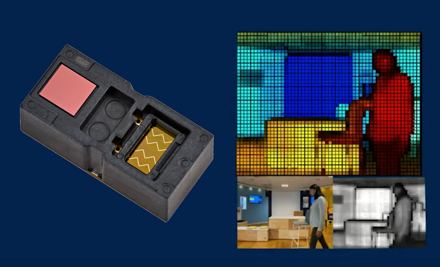
For example, a fall detection system for elder care might not need to identify a person’s face. This could bring intelligent sensing not just closer to home, but to personal spaces too.
Future Machines That Will Sense Their SurroundingsThe technology we are being treated to in the newest ST report indicates an imaging future much broader than just pretty pictures. The attention turns to machine vision, AI, depth sensing, low-power computing and real-time perception. The company’s portfolio includes the new low-power and 5-megapixel Bright Sense sensors targeting edge AI, wearables and industrial automation. Its Flight Sense technology delivers 3D sensing to the edge for a number of uses ranging from robots to smart buildings.
It’s part of a much larger technology trend. AI isn’t confined to your computer screen anymore; it’s becoming a physical part of the physical world around us. In robotics, drones, smart machines, vehicles, or the large number of interconnected gadgets and gizmos out there, it’s important for something to know the difference between the road and your living room before they do something smart (or frankly, dangerous). And that’s why intelligent sensors are becoming so valuable. The biggest revolution of all might be that machines can at last see. And this is where the real revolution is- they are starting to understand what it is that they see.
As the power of Edge AI grows and sensors are becoming smaller, smarter, and more energy efficient, the devices around us may soon have the capability to detect the changes around them, understand them, and react to them in the right way. Perhaps the future of AI won’t involve only smarter software. It would also depend on providing machines with appropriate vision, appropriate senses, and the ability to understand the world around them.
The post From Seeing to Perceiving: How STMicroelectronics is Teaching Machines a New Sense of Perception appeared first on ELE Times.
Lumentum’s president & CEO to receive Optica i4 Individual Achievement Prize
Keysight Certifies Electromagnetic Design Software for Intel Foundry’s Latest Processes
Keysight Technologies, Inc. today announced certification of its RFPro electromagnetic (EM) design software, part of the Keysight EDA Advanced Design System (ADS), for Intel 14A and Intel 18A-P process technologies. The certification gives radio frequency integrated circuit (RFIC) and mixed-signal designers confidence that their electromagnetic simulations accurately reflect Intel Foundry’s latest manufacturing processes before chips move to production.
As semiconductor manufacturers introduce increasingly advanced process technologies, design teams face growing pressure to shorten development cycles while avoiding costly design errors. Certified simulation software enables engineers to identify and resolve performance issues before manufacturing begins, helping reduce development risk, avoid expensive chip redesigns and accelerate time to market.
A mismatch between EM and circuit behavior that surfaces only after tape-out means an expensive re-spin, so simulation tools must be validated on a node before design work begins. Keysight’s certification gives teams that path as Intel Foundry delivers on its roadmap from Intel 18A into 18A-P and Intel 14A, which introduces RibbonFET 2 and PowerDirect, its new transistor and power delivery architectures.
This certification builds on Keysight’s ongoing collaboration with Intel Foundry, including support for Intel 18A and EMIB-T advanced packaging technology. Together, these capabilities provide customers with consistent design flows across multiple Intel process generations, supporting applications ranging from AI and high-performance computing to mobile devices.
Shawn Han, Senior Vice President and General Manager, Foundry Services, Intel Corporation, said: “As our customers look to address next-generation demands through differentiated solutions, Intel Foundry believes predictable execution on our advanced process and packaging technologies will accelerate their innovation,” “By collaborating closely with ecosystem partners such as Keysight to certify world-class solutions, we are providing our customers with greater confidence they can achieve their power, performance and efficiency goals and get to market more quickly.”
Niels Faché, Senior Vice President, Keysight Design Engineering Software, said: “Design teams can’t wait for a new process node to mature before they trust their simulation results. This certification means engineers can adopt Intel Foundry’s newest technologies early and get the silicon right the first time.”
The post Keysight Certifies Electromagnetic Design Software for Intel Foundry’s Latest Processes appeared first on ELE Times.
EDOM Accelerates Edge AI Deployment with NVIDIA Technologies
EDOM Technology, Asia’s best solutions provider, today announced an expanded collaboration with NVIDIA to help enterprises accelerate Edge AI adoption by integrating the NVIDIA Edge AI platform, open-source models, and system optimization technologies. The collaboration enables organizations to lower the barriers to deploying large AI models while reducing overall deployment costs.
As generative AI rapidly evolves from proof-of-concept to real-world applications, enterprise priorities are shifting. Rather than simply pursuing larger AI models, organizations are increasingly focused on running AI reliably on existing hardware platforms, accelerating deployment, and maximizing return on investment. Across industries from smart manufacturing and autonomous robotics to healthcare, Edge AI has become a key driver of digital transformation where efficient deployment is critical to successfully bringing AI projects into production.
The way enterprises adopt AI is also changing. Instead of building models from scratch, organizations are increasingly leveraging mature foundation models and open-source AI ecosystems to accelerate development, followed by application specific optimization and deployment. However, as AI models continue to grow in capability, several deployment challenges such as memory capacity, inference performance, and system integration have become major hurdles.
EDOM addresses these challenges by combining the NVIDIA Jetson platform with NVIDIA JetPack, NVIDIA CUDA, NVIDIA TensorRT, NVIDIA Jetson AI Lab, and leading open-source AI models and inference frameworks. The company delivers a comprehensive portfolio of services spanning platform selection, model integration, model quantization, memory optimization, and system validation. This end-to-end approach enables enterprises to maximize hardware resource utilization, reduce deployment costs, and shorten the journey from proof of concept (PoC) to production.
A notable example is NVIDIA Reachy Mini Jetson Assistant, which demonstrates how Headless Mode, NVIDIA Cosmos-Reason2 open VLMs, model quantization, and optimized inference frameworks enable multimodal AI workloads—including vison- language reasoning, Speech-to-Text (STT), and Text-to-Speech (TTS)—to run simultaneously on the NVIDIA Jetson Orin Nano 8GB platform. This showcases how software and system optimization can efficiently execute multiple AI models and reduce memory footprint on resource-constrained edge devices. Similar architectures are increasingly being adopted across smart manufacturing, autonomous robotics, and healthcare applications, supporting use cases such as production line inspection, intelligent vision systems, voice-enabled interaction, and autonomous decision-making. By performing AI inference directly on edge devices, organizations can achieve low-latency performance while enhancing data security and operational efficiency.
“Generative AI has entered the stage of real-world deployment,” said Jeffrey Yu, CEO of EDOM Technology. “Today, the biggest challenge for enterprises is no longer finding AI models; it’s successfully deploying AI into products and operational environments. The success of an AI project depends not only on hardware performance, but also on deployment efficiency, system integration capabilities, and overall return on investment. EDOM’s role extends beyond supplying platforms and components. We help customers integrate NVIDIA technologies, open-source AI models, and system optimization strategies to accelerate time-to-market, reduce deployment risks, and enable AI to deliver measurable business value.”
Backed by years of expertise in Edge AI and embedded system integration, EDOM provides end-to-end solutions encompassing selections powered by NVIDIA technologies, open-source AI models integration and application optimization, hardware design, and system deployment. The company has successfully enabled Edge AI applications across smart manufacturing, autonomous robotics, healthcare, smart retail, and smart city initiatives. Looking ahead, EDOM will continue collaborating with NVIDIA and the open-source AI community to help enterprises overcome the challenges of deploying large AI models, accelerate the transition from proof of concept to large-scale deployment, and transform AI innovation into tangible value across the industry value chain.
The post EDOM Accelerates Edge AI Deployment with NVIDIA Technologies appeared first on ELE Times.
Uttar Pradesh Emerges as India’s Biggest Electronics Hub, Producing 65% of the Nation’s Mobile Phones
Uttar Pradesh has emerged as India’s leading electronics manufacturing hub, producing nearly 65% of the country’s mobile phones. Driven by strong investments, industry-friendly government policies, and the rapid expansion of manufacturing facilities, the state has become a major centre for electronics manufacturing and mobile phone production.
Since 2014, UP has been a hotspot for electronic manufacturers, including domestic and international ones to invest particularly in the Noida-Greater Noida-Yamuna Expressway corridor. Global big manufacturing smartphones, as also their component suppliers, have built huge manufacturing units in the area and put up a complete electronics manufacturing value chain. The state government says it accounts for roughly 65% of all mobile phones being manufactured in the country and is India’s biggest base for smartphone production.
Multiple efforts by both central and state governments have assisted the growth of the electronics sector in the state of Uttar Pradesh. At the national level, policies like the Production Linked Incentive (PLI) Scheme for large electronics manufacturing incentives; the setting up and scaling of production capacities in India, whereas the electronics manufacturing policy issued by the state offers supplemental incentives, enhanced infrastructure, and business ease reforms.
The proactive actions of the Uttar Pradesh government to streamline approvals, build an efficient logistics infrastructure, boost investor confidence, and encourage (foreign direct investment) FDI have positioned the state as a prominent investment destination for the global electronics sector.
While these efforts should result in significant acceleration of manufacturing and investment in UP, the state has a lot of work ahead of itself in achieving sustained future growth. Increasing domestic value addition; further ramping up production of semiconductors and components; creating an ecosystem of highly skilled personnel; and upgrading research and development to enhance in-house R&D is crucial for a long-term plan. To stay competitive globally, UP will also need to make priority investments, to ensure availability of dependable power supply, a world-class logistics system, and highly advanced manufacturing technologies.
The post Uttar Pradesh Emerges as India’s Biggest Electronics Hub, Producing 65% of the Nation’s Mobile Phones appeared first on ELE Times.
Rapid scale-up in data center: The case for distributed optical circuit switching

AI infrastructure is moving from server-scale acceleration to multi-rack supernodes that must behave like a single, highly available computer. Distributed optical circuit switching offers a practical way to extend scale-up fabrics with lower latency, lower power, flexible topology control, and limited disruption to existing data center architecture.
AI data centers are entering a phase where the hardest problem is not simply building a faster accelerator. It’s keeping thousands of accelerators fed, synchronized, and available as one machine. Training frontier models, serving long-context inference, and running agentic workloads all create a similar demand: more devices must communicate over longer distances without allowing the network to dominate cost, latency, power, or reliability.
That changes the definition of scale-up. It’s no longer only the set of links inside a server or rack. Increasingly, scale-up must span multiple racks while preserving the low-latency behavior programmers expect from a tightly coupled system.
Nvidia has framed the issue in similar terms, noting that as AI factories reach “extreme scale,” networking infrastructure “must be reinvented to keep pace.” The company’s recent silicon photonics announcements focus on exactly the metrics now becoming critical in AI infrastructure: power efficiency, signal integrity, resilience, and deployment speed.
That emphasis reflects a broader industry shift. The bottleneck is no longer just whether a link can move bits from one endpoint to another. It’s whether the entire fabric can support large, tightly synchronized accelerator domains while reducing power, limiting failure points, and remaining practical to deploy and service.
Copper has been the default for scale-up because it’s familiar, low latency, and economical at short reach, but physics is becoming less forgiving as per-lane data rates rise. Longer copper paths increase insertion loss and signal-integrity burden; thicker wires help the signal but work against density, airflow, and manufacturability.
Rack-scale cable trays become difficult to assemble and service, and a failure may require replacing large mechanical units rather than a small module. Retimers, equalization, and more complex board design can extend the life of copper, but they do not remove the underlying reach-density-power tradeoff.
Traditional pluggable optics solve part of this problem. They move data farther with less distance penalty than copper and are widely deployed in scale-out networks. But a scale-up fabric is different from a scale-out Ethernet fabric. Scale-up traffic often has stricter latency, synchronization, and collective-communication requirements, and in emerging architectures may carry memory-semantic traffic rather than ordinary packetized network traffic.
In that environment, the raw specifications of an optical link alone are not sufficient. The fabric also needs deterministic paths, fast reconfiguration, high serviceability, and smaller, more containable failure domains.

Figure 1 Next-generation scale-up and scale-out solutions extend the limits of traditional electrical interconnect and pluggable optical modules. Source: Lightelligence
Co-packaged optics (CPO) is an important long-term solution, but it’s not a simple drop-in replacement for today’s data center designs. Bringing optical engines into or near the package changes the thermal, packaging, manufacturing, serviceability, and qualification model. Recent industry discussions around CPO focus heavily on these operational issues: how to manufacture high-yield optical assemblies, make optical interfaces field-serviceable, and manage light sources and redundancy at scale.
Nvidia’s recent Spectrum-X Ethernet Photonics announcements also show where early CPO commercialization is gaining traction: scale-out and scale-across AI-factory networking. Scale-up CPO will follow, but it asks a different question: how do we preserve the behavior of a tightly coupled compute domain while changing the physical medium underneath it?
This is where distributed optical circuit switching, or dOCS, becomes important. Rather than concentrating the switching function in precious rack space, a dOCS architecture distributes compact silicon-photonic switching elements close to servers, GPU trays, or XPU clusters. This improves compute density by eliminating the switch chassis.
The goal is to keep data in the optical domain from port to port through the switch path, reducing unnecessary optical-electrical-optical conversions and avoiding the power and cost burden of very large centralized electrical switch ASICs. In practical terms, dOCS treats the scale-up network less like a fixed cable plant and more like a configurable optical fabric.

Figure 2 A distributed optical circuit switch (dOCS) integrates the optical interconnect and switching functions into one compact module. Source: Lightelligence
The distinction matters. A centralized switch can become expensive, power-intensive, and operationally painful as scale-up domains grow. It can also create a large failure domain. A distributed optical switch breaks the switching function into smaller modules, shrinking the blast radius of any one failure and enabling more granular service.
In one described implementation, the dOCS module integrates optical interconnect and optical circuit-switching functions in a compact module built around silicon photonics, controller, driver, and receiver circuitry. The architecture is intended to support millisecond-level failover, including substitution of a hot-standby GPU when a device fails.
For AI workloads, the value of that reconfigurability is not only resilience, it’s also topology control. Different phases of training and inference stress the fabric differently.
Dense all-reduce operations, mixture-of-experts routing, retrieval, key value (KV)-cache movement, and pipeline-parallel execution do not all benefit from the same topology. A circuit-switched optical layer can expose topologies such as ring, mesh, or dragonfly and allow the cluster manager to adjust the fabric according to specific workload-parallelism requirements.
Recent dOCS-based supernode work has described real-time topology reconfiguration and elastic expansion beyond 500 GPUs in a single logical domain. The broader architectural point is more important than the exact number: the network should become a schedulable resource, not a static constraint.
This also helps explain why dOCS is especially relevant to certain architectures. A supernode is not just a cluster with a marketing label. It is a tightly interconnected group of GPUs or other accelerators that attempts to behave like one large compute unit. In that context, effective model FLOPs utilization depends on how much time accelerators spend computing rather than waiting.
Optical scale-up links can extend reach across racks, while circuit switching can create predictable paths for high-volume collective traffic. The result is not simply more bandwidth on a datasheet; it’s a path to higher sustained utilization.
The same argument applies to memory. AI systems are increasingly constrained by memory capacity, memory bandwidth, and the location of memory relative to compute. High-bandwidth memory (HBM) on the accelerator remains essential, but it’s finite and expensive. Long-context inference and agentic workloads amplify the pressure by generating large KV caches and preserving more state across interactions.
CXL is important because it provides cache-coherent connectivity for processors, memory expansion, and accelerators, enabling resource sharing with lower software complexity. But coherent memory fabrics still need physical reach. Optical PCIe/CXL links and reconfigurable optical switching can help move memory from a stranded local resource toward a pooled resource available across boards, servers, and racks.
The practical advantage of dOCS is that it creates an intermediate deployment path. Data center operators do not need to redesign every server, change every protocol, or wait for full CPO maturity before gaining optical reach and switching flexibility in the scale-up domain. A dOCS-based fabric can be designed to remain protocol agnostic at the physical layer, supporting multiple higher-level fabrics while changing the transmission medium and switching mechanism underneath.
That matters because AI data centers are heterogeneous. They include GPUs, CPUs, XPUs, switches, storage, memory expansion devices, and management controllers sourced from multiple vendors and refreshed on different schedules.

Figure 3 As shown in this example, the dOCS architecture offers a practical advantage by creating an intermediate deployment path. Source: Lightelligence
A sensible roadmap is therefore not copper versus CPO, or pluggables versus CPO. It’s a staged migration. Linear pluggable optics can address immediate reach and power issues with limited architectural change. Distributed optical circuit switching can add fabric-level reconfiguration, availability, and scale-up reach.
Near-packaged optics can shorten electrical traces and improve density. CPO optics can eventually move optical I/O directly beside GPUs or switch ASICs for the highest bandwidth density and lowest electrical loss. Each step moves optics closer to the compute, but each step should also preserve serviceability and operational practicality.
The AI infrastructure industry is learning a familiar lesson from earlier computing transitions: the winning technology is rarely the one with the most elegant device physics alone. It’s the one that fits into systems, software, manufacturing, and operations at the right time.
The dOCS architecture fits that requirement because it attacks a real bottleneck now. It extends scale-up beyond the practical limits of copper, avoids inefficiencies of repeated electrical conversion, supports flexible accelerator-fabric topologies, and improves system uptime by localizing failures and rapidly rerouting traffic or switching to standby resources when hardware fails.
The future data center will almost certainly use several optical technologies at once: pluggable optics, linear drive optics, near-packaged optics, CPO, optical I/O chiplets, CXL-enabled memory fabrics, and optical circuit switches. The case for dOCS is that it gives operators a rapid-deploy scale-up option while the rest of the optical roadmap matures.
For AI infrastructure, that may be the most important kind of innovation: not a clean-sheet replacement for the data center, but a way to make the next supernode larger, more efficient, more available, and easier to deploy than the last one.
 Maurice (Mo) Steinman is senior VP and U.S. GM at Lightelligence. He has enjoyed a 40-year career in the semiconductor industry, working for such companies as Digital, Compaq, HP, Intel and AMD, where he held the title of Senior Fellow before joining Lightelligence. Steinman has expertise in SoC architecture, SoC interconnect, memory subsystems, and energy management.
Related Content
- Optical switches primed for test debut
- The advent of co-packaged optics (CPO) in 2025
- Building Optical Control Planes: Challenges and Solutions
- Where co-packaged optics (CPO) technology stands in 2026
- Overcoming interconnect obstacles with co-packaged optics (CPO)
The post Rapid scale-up in data center: The case for distributed optical circuit switching appeared first on EDN.
Сторінки




![[link]](https://i.redd.it/2188cu66c5gh1.png)