


Збирач потоків
DNA-Powered Memory Could Cut Computing Energy Use by 100x
A team of researchers at Penn State University has now come up with a bio-hybrid device that pairs custom-synthesised human DNA with a perovskite crystalline semiconductor to present a new form of low-power data storage and computation. Their study was published in Advanced Functional Materials in the latest edition released August 17, 2026. Such a device may in time help reduce the energy used for powering AI computing centres and huge data centres, the scientists say.
The technology addresses a growing challenge in modern computing: the enormous energy required to model and process data. An increasing number of high-performance AI workloads and the overall compute and memory demand of data centres mean that there is pressure to find a more efficient way to store and process data.
The researchers used synthetic DNA – a chemically engineered molecule arranged into short molecular sequences and a crystalline perovskite semiconductor material (used in things like solar cells and electronics). The combined pair of these materials created a memristor: a type of electronic memory that retains clues about its past electrical experience.
Such technology could potentially go toward energy-efficient AI-computing hardware; as well as data centres and even the burgeoning field of neuromorphic computing by coupling the storage and processing information within the same device.
The development highlights a broader trend in semiconductor research: instead of relying solely on conventional silicon scaling, researchers are exploring biological materials, memristors and unconventional computing architectures to address the energy and memory demands of next-generation AI systems.
The post DNA-Powered Memory Could Cut Computing Energy Use by 100x appeared first on ELE Times.
Nuvoton Launches Mass Production of 16-Cell Battery Monitoring ICs with Daisy-Chain Communication for AI Servers
Nuvoton Technology is preparing to begin mass production of its KA49703A and KA49713A battery monitoring ICs (BMICs) in September 2026. The devices are designed for Battery Backup Units (BBUs) used in AI servers, helping monitor battery-cell conditions and support reliable power management in high-performance computing systems. As AI servers become critical infrastructure supporting modern society, ensuring continuous operation requires highly reliable power systems capable of running 24/7 throughout the year. By leveraging the company’s proven automotive-grade daisy-chain communication technology in high-voltage 400V/800V BBU applications, the KA49703A and KA49713A help realize highly reliable and efficient power architecture.
Achievements:
1. Supports daisy-chain communication and connection of up to 55 devices, simplifying large-scale battery system design.
2. Incorporates a transportation and storage mode that extends storage duration and reduces operational costs.
Data centers are mission-critical infrastructure that must operate continuously without interruption. Consequently, their power systems require exceptional reliability and stability. In recent years, the rapid growth of generative AI and cloud services has significantly increased AI server power consumption, driving demand for higher efficiency and reliability in power delivery systems.
At the same time, adoption of 400V and 800V high-voltage power architectures is accelerating to improve power efficiency,
while server and power-system densities continue to increase. These trends require battery systems not only to provide safe
monitoring under high-voltage conditions but also to ensure long-term reliability and low thermal generation during continuous
operation.
Battery systems are no longer simply backup power sources for outages. They now play an increasingly important role in
absorbing instantaneous power fluctuations, protecting systems, and ensuring service continuity, making them foundational
technologies for modern data centers and communication infrastructure.
Building on its proven automotive daisy-chain communication technology, Nuvoton has developed the KA49703A and KA49713A battery monitoring ICs for high-voltage 400V/800V BBUs used in industrial and infrastructure applications. Mass production is scheduled to begin in September 2026.
The KA49703A and KA49713A can accurately monitor up to 16 battery cells while integrating communication functions for high- voltage systems and safety features such as cell anomaly detection, addressing the demanding requirements of next generation energy storage systems.
Features of New Product:
1. Daisy-Chain Communication Supporting up to 55 Devices
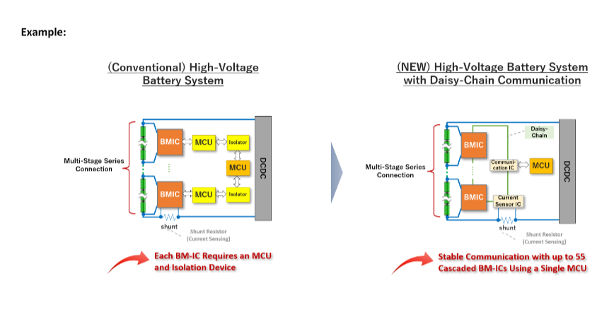
AI-server BBUs and Energy Storage Systems (ESS ) operating at 400V/800V levels require large numbers of lithium-ion battery cells connected in series. Conventional battery monitoring systems typically require a dedicated MCU and isolation device for each monitoring IC. As cell counts increase, component count and communication wiring also increase, creating challenges in communication reliability and system complexity.
To address these issues, the KA49703A and KA49713A incorporate daisy-chain communication technology. Multiple battery monitoring ICs can be connected in series, enabling systems with up to 55 devices while minimizing wiring requirements and ensuring robust communication even in high-voltage environments. This architecture reduces the need for additional MCUs and isolation components, simplifying system design, reducing component count, minimizing board space, and improving overall reliability. The compact QFP-48 package (7 mm × 7 mm) also helps address the stringent space constraints found in AI server BBUs. Combined with high-precision voltage measurement accuracy of ±2.9 mV, the device enhances both monitoring performance and safety in next-generation power systems.
2. Transportation and Storage Mode Reduces Maintenance Costs
AI-server BBUs and large-scale ESS installations contain numerous lithium-ion cells and are often transported over long distances by ship or truck. Minimizing power consumption during transportation and storage is therefore essential.
However, conventional ICs incorporating daisy-chain communication typically exhibit increased shutdown current, leading to
battery drain during storage and transport.
To solve this issue, the KA49713A incorporates a dedicated transportation and storage mode that reduces shutdown current to less than 0.1 μA.
This significantly minimizes battery depletion during transportation and storage, extends allowable storage periods, reduces recharge requirements, and contributes to lower operating costs.
These battery monitoring ICs enable customers to address increasing power demands in the AI era and the transition toward higher-voltage power systems. They support improved reliability and operational efficiency in energy storage systems for data centers, industrial equipment, and social infrastructure.
Through continued expansion of its BM-IC product lineup, Nuvoton will further advance battery monitoring technologies and contribute to realizing a sustainable and highly reliable energy society.
Applications:
・Battery Backup Units (BBUs) for AI servers
・Large-scale Energy Storage Systems (ESS)
Product name:
Industrial Battery Monitoring ICs
・KA49703A
・KA49713A
Specifications:
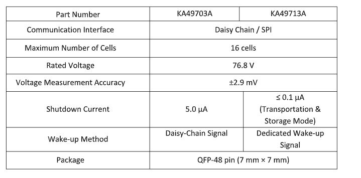
Start of mass production:
Sep. 2026
Definitions:
- BBU (Battery Backup Unit). A backup power system equipped with rechargeable batteries, such as lithium-ion batteries, that supplies power during outages or momentary voltage drops.
- Daisy-Chain Communication. A communication method in which multiple monitoring ICs are connected in series. It reduces wiring complexity while providing high immunity to electrical noise.
- ESS (Energy Storage System). An energy storage system used for renewable energy integration, peak load management, and power supply-demand balancing.
The post Nuvoton Launches Mass Production of 16-Cell Battery Monitoring ICs with Daisy-Chain Communication for AI Servers appeared first on ELE Times.
Older multitap can capactors, replacement option.
 | I read the different values on each tap in can capactor the get a single matching cap with equal or greater voltage and temp. Then set them as you see on a daughterboard, binding all grounds to a common ground post. Then run wiring to the appropiate terminal or junction of where that value capactor was in the circuit before. I find this way an efficient and orderly way to replace older multi-can capactors. The daughter board is attached to chassis by one or two small, "L" brackets. [link] [comments] |
Ascent Solar broadens thin-film space PV testing beyond NASA’s low Earth orbit results
🎓 Додатковий набір до КПІ ім. Ігоря Сікорського на бакалаврат

У вересні КПІ проводить додатковий набір вступників на навчання за кошти фізичних та/або юридичних осіб (контракт).
AI silicon: Package becoming system architecture

The future of advanced packaging is not one universal package. It’s a technology platform capable of placing the right interconnect, material, die, memory stack, optical engine, and thermal structure at the right system boundary.
For many years, the design sequence appeared straightforward:
Design the chip → select the package → connect it to the board
That sequence is becoming less accurate. AI accelerators, high-bandwidth memory (HBM), chiplets, optical I/O, advanced cooling, and high-current power delivery are now so tightly coupled that the package can no longer be selected after the system architecture is largely complete.
The package increasingly determines:
- How the system can be partitioned
- How many chiplets can be integrated
- Where silicon-class interconnect density is required
- Where broader and lower-cost routing is sufficient
- How HBM is placed and connected
- Where electrical path should transition to optic
- How power reaches the compute elements
- How heat leaves the package
- How assembly can be manufactured, tested, repaired, and qualified
The package is no longer merely supporting the system. It’s defining what system can be built.
From package choice to packaging platform
Traditional packaging discussions often compare individual technologies:
- Should the design use a silicon interposer?
- Would a local silicon bridge be sufficient?
- Should fan-out redistribution replace part of the substrate?
- Should the system use 2.5D or 3D integration?
- Should optics remain at the front panel, move near the package, or become co-packaged?
These remain important questions, but they are no longer independent choices. A modern AI system may require several of these technologies at the same time.
A broad interposer may connect compute chiplets and HBM. Here, localized bridges may provide silicon-class density only at selected die boundaries. And fan-out redistribution may extend routing across a larger area. Next, vertical stacking may integrate cache, memory, control, or specialized processing. Then there are optical engines that may sit near the package edge.
A thermal structure may also need to remove highly non-uniform heat from several dies with different power densities. Finally, the system may also require test access, known-good-die strategies, repair paths, redundancy, and manufacturing flows that span several suppliers. This is why advanced packaging is moving from isolated process choices toward integrated technology platforms.
A platform does not force every product into one structure. It provides a coordinated set of technologies from which the system architect can select the right realization method for each boundary.
Vertical integration’s two meanings
The phrase vertical integration is often interpreted physically. But that is the first meaning.
Physical vertical integration
Dies, memory stacks, interconnect layers, optical engines, power-delivery structures, and thermal components are placed beside or above one another. This includes technologies such as:
- 2.5D integration
- 3D die stacking
- Package-on-package structures
- Through-silicon or through-glass vias
- Vertically-integrated power delivery
- Stacked memory and logic
Physical stacking is important because it can shorten interconnects, increase bandwidth density, reduce footprint, and place functions closer together. But there is a second meaning that may be even more important.
Technology platform integration
Different packaging technologies become coordinated elements within one ecosystem. A platform may combine:
- Broad-area fan-out routing
- Localized silicon bridges
- Full silicon interposers
- Vertical stacking
- System-in-package integration
- Co-packaged optics
- Assembly and bonding processes
- Package-level test
- Thermal and mechanical structures
- Manufacturing and reliability flows
In this model, vertical integration does not mean that every component must be stacked. It means the complete realization capability is integrated across design, materials, process, assembly, test, and system requirements. That is the deeper transition.
In other words, the future is not one package replacing all others. It’s a platform selecting the right precision, material, and integration method at each boundary.
Different boundaries need different precision
One of the most important architectural questions is: How much of the package truly requires silicon-class interconnect density?
A full silicon interposer can provide extremely dense routing and short connections across a broad area. But that precision comes with cost, area, yield, manufacturing, and mechanical consequences. Not every connection requires the same pitch or routing density.
Some die-to-die boundaries may require very fine-pitch interconnect. Other regions may only need moderate-density redistribution. Still others may be adequately served by an organic substrate or board-level connection.
A platform approach allows the package to become hierarchical: Silicon-class density where necessary.
- Fan-out or redistribution where broader routing is needed
- Substrate-level routing where lower density is sufficient
This avoids using the most expensive and complex technology everywhere. The objective is not maximum integration at every location; the objective is appropriate integration at every boundary.
Fan-out more than a package format
Fan-out packaging is often discussed as a package category. But within a larger platform, fan-out can perform several architectural roles. It can:
- Provide broad redistribution beyond the original die footprint
- Support heterogeneous die integration
- Reduce dependence on a large silicon interposer
- Connect local high-density regions to broader package routing
- Create a transition between chiplet-scale and substrate-scale interconnect
- Support system-in-package or package-on-package structures
Fan-out chip-on-substrate approaches can combine redistribution-layer density with the mechanical and routing capabilities of a larger package substrate. A fan-out bridge architecture can place localized silicon-class interconnect only where adjacent dies require it.
This allows precision to be concentrated rather than distributed uniformly across the complete package. That is not simply a manufacturing variation; it’s an architectural choice about where density should reside.
Bridges and interposers are complementary
Silicon bridges and full interposers are sometimes presented as competing technologies. They are better understood as different tools.
A broad interposer can provide:
- Dense routing across a large region
- Extensive die-to-die connectivity
- Controlled electrical paths
- Close integration between compute and HBM
- Broad placement flexibility
A local bridge can provide:
- Very high density at selected chiplet boundaries
- Reduced silicon area
- More localized precision
- Potentially lower cost for systems that do not require a full interposer
- A path to combine high-density and conventional routing within one package
The correct decision depends on:
- Die placemen
- Required pitch
- Routing density
- Signal reach
- Power delivery
- Thermal expansion
- Warpage
- Assembly tolerance
- Yield
- Test
- Cost
A packaging platform should therefore not declare one technology universally superior. It should allow the architecture to place each technology where it creates the greatest system value.
HBM makes package a compute boundary
HBM has already transformed the package. The connection between the accelerator and HBM is no longer a peripheral interface; it’s part of the compute architecture.
HBM placement determines:
- Achievable bandwidth
- Energy per bit
- Interposer or bridge requirements
- Package area
- Routing density
- Power delivery
- Thermal interaction
- Mechanical balance
- Yield and assembly complexity
As the number of HBM stacks grows, the package becomes larger and more difficult to manufacture. So, the system must manage:
- Interposer scale
- Reticle boundaries
- Die placement accuracy
- Warpage
- Underfill
- Bump reliability
- Heat-spreader geometry
- Non-uniform thermal loading
- Package-level test
The package is therefore not merely connecting compute to memory. It’s determining the physical shape of the compute system.
CPO an element of the platform
Co-packaged optics (CPO) is often treated as a separate technology story. But CPO cannot scale independently from advanced packaging. Moving the optical engine closer to a switch ASIC or accelerator may reduce electrical reach, SerDes power, and front-panel density pressure.
It also introduces new package-level responsibilities:
- EIC-to-PIC connectivity
- Optical attach
- Fiber routing
- Laser placement
- Wavelength control
- Thermal drift
- Calibration
- Optical test
- Compound yield
- Repairability
- Serviceability
A future AI package may combine:
- Compute dies
- HBM
- A full or partial interposer
- Localized bridges
- Fan-out redistribution
- Electrical I/O chiplets
- Optical engines
- External laser interfaces
- Power delivery structures
- Integrated cooling
CPO is therefore not simply another component added beside the ASIC. It changes the electrical, thermal, mechanical, manufacturing, test, and serviceability boundaries of the complete package. However, the package must create the environment in which optical performance can ensure repeatable system performance.
Optics moves inward only when the package platform can absorb the consequences of moving it inward. This is why CPO belongs inside the larger packaging-platform discussion.
Thermal architecture chosen with the package
As more functions move into the package, thermal design can no longer be treated as an external cooling problem. Different dies produce different heat fluxes. HBM, compute chiplets, I/O dies, optical engines, voltage-regulation structures, and control electronics may all have different temperature limits.
The package architecture determines:
- Which devices share a heat spreader
- Where thermal-interface materials are placed
- How bond-line thickness is controlled
- Whether a lid, cold plate, vapor chamber, or direct-liquid structure is required
- How mechanical pressure is distributed
- How thermal expansion affects interconnect reliability
- Whether optical alignment drifts with temperature
A package platform must therefore support more than electrical connectivity. It must coordinate the thermal path with the die placement, interconnect architecture, assembly process, and reliability requirements.
The best electrical placement may not be the best thermal placement; the best thermal placement may complicate fiber routing or package test. This is why package architecture is a system trade-off, not an isolated layout decision.
Power delivery also a package decision
AI systems require large current with rapidly changing load demand. As package power rises, the distance between voltage regulation, decoupling, power planes, and compute dies becomes increasingly important.
So, the package may need:
- Improved vertical power delivery
- Backside or near-die power structures
- Integrated voltage regulation
- Lower-inductance current paths
- More distributed decoupling
- Coordinated signal and return-current design
Power delivery interacts with:
- Chiplet placement
- HBM placement
- Interposer routing
- Thermal density
- Mechanical structure
- Package height
- Available routing layers
Manufacturing and test platforms
A package can be electrically attractive and still be difficult to manufacture. A platform approach must connect architecture choices to process capability. Questions include:
- Can the required die-placement tolerance be achieved?
- Can the redistribution layers be fabricated at the required scale and yield?
- Can the bridge or interposer be assembled without unacceptable warpage?
- Can underfill penetrate the available stand-off?
- Can thermal stack be controlled within bond-line limits?
- Can optical interface survive assembly and thermal cycling?
- Can each die be tested before integration?
- Can the completed assembly be tested after integration?
- Can failed modules be repaired or replaced?
- Can failed modules be repaired or replaced?
The package architecture is not complete when the drawing is complete. It’s complete when the process can repeatedly produce the intended geometry and performance. Manufacturing does not merely build the package; it creates the physical structure through which the system must operate.
Next, as the number of integrated dies increases, test complexity grows rapidly. A platform must account for:
- Known-good-die requirements
- Pre-bond test
- Post-bond test
- Interposer and bridge continuity
- Memory test
- Optical loopback
- Thermal calibration
- Power-delivery validation
- Fault isolation
- Repair or redundancy strategies
The challenge is especially severe when dies from different suppliers are integrated into one product. A failure in one small component can affect the yield of the entire assembly. This creates a compound-yield problem.
The value of a platform is therefore not simply that it offers several package technologies. It should also provide coordinated design rules, assembly flows, test access, metrology, failure analysis, and reliability evidence across those technologies.
System architecture now begins with workload
The new design sequence should begin with the workload and move downward into physical realization. Here, the deterministic chain encompasses:
- Workload requirements
- System partitioning
- Compute and memory placement
- Electrical and optical boundaries
- Package architecture
- Power and thermal architecture
- Manufacturing and test strategy
- Verified system performance
This reverses the older assumption that the package is selected near the end. The package platform must be taken into consideration from the beginning because it defines which partitioning options are physically and economically possible. A system architect cannot decide where compute, memory, optics, and power should reside without understanding the package technologies available to connect and sustain them.
Platform is not product
There is one important caution. A large portfolio of packaging technologies does not automatically produce a successful AI system. The platform provides options, but the product must still select and coordinate them correctly.
Adding more technologies can also increase:
- Process interactions
- Supplier dependencies
- Yield risk
- Test complexity
- Thermal coupling
- Mechanical stress
- Qualification burden
- Cost
The winning package will not be the one that includes the greatest number of advanced technologies. It will be the one that uses each technology only where its benefit exceeds its integration burden.
A local bridge may be better than a full interposer in one system. A full interposer may be essential in another. Near-packaged optical (NPO) may provide the right optical boundary for one product and CPO may be justified for another.
Vertical stacking may reduce latency but worsen thermal density. Fan-out may reduce cost but impose different warpage and process constraints. Therefore, the architecture must be selected based on system evidence, not technology enthusiasm.
Advanced packaging is no longer a menu of isolated process choices. It’s becoming the architecture through which compute, memory, electrical interconnect, optics, power delivery, cooling, manufacturing, and test are assembled into one realizable system.
The future is not one universal package. It’s an integrated technology platform capable of placing:
- Silicon-class density where it’s necessary
- Broader redistribution where it’s sufficient
- Vertical stacking where proximity creates value
- Optics where electrical reach becomes limiting
- Cooling where heat is generated
- Test access where failure must be isolated
The package is no longer selected after the system is defined. It increasingly determines which system architecture can be realized, manufactured, qualified, and scaled. The winning platform will not be the one that stacks the most technologies. It will be the one that places each technology where its system benefit exceeds its realization burden.
The chip defines capability. The package platform defines the system.
Dr. Moh Kolbehdari is senior director of IC/packaging at Socionext US.
Related Content
- True Wafer-Level Packaging
- Wafer Level Chip Size Package (WLCSP) Guidelines
- Intel’s Embarrassment of Riches: Advanced Packaging
- Nvidia, TSMC, and advanced packaging realignment in 2025
- Intel flash move could put wafer-level packages on the map
The post AI silicon: Package becoming system architecture appeared first on EDN.
Op-amp LC oscillator uses tank losses for amplitude stabilization

This proposed design eliminates traditional additional requirements for AGC, AC coupling, and post amplification circuitry.
This Design Idea presents a simple op-amp-based sine wave oscillator that directly generates a low-impedance bipolar output of approximately 20 Vpp at frequencies above 100 kHz. The circuit was developed to directly drive an AD633 in an on–off keying (OOK) digital transmission system.
Wow the engineering world with your unique design: Design Ideas Submission Guide
Many sinewave oscillators reported in the literature provide a unipolar output and require additional circuitry for automatic gain control (AGC), AC coupling, and post amplification to achieve the desired amplitude. The proposed circuit eliminates these requirements by directly generating a high-amplitude bipolar sinewave.
The circuit (Figure 1) consists of an LC tank connected in a feedback loop with an op-amp configured as an inverting amplifier with a gain set by the R3/R2 ratio. At the resonance frequency, fosc = 1/(2π√(L·Cs)), where Cs = C1 || C2, the LC network introduces 180° phase shift, while the inverting amplifier provides an additional 180°, resulting in a total loop phase shift of 360°, thus satisfying the Barkhausen phase condition.

Figure 1 This simple LC oscillator uses an op-amp and the intrinsic losses of the resonant tank to generate a stable low-distortion 20 Vpp sine wave without AGC.
The topology can be viewed as a simplified Colpitts oscillator in which the op-amp both sustains oscillation and compensates for the losses of the resonant network. A key practical advantage is that the oscillation amplitude is set by the op-amp closed-loop gain, primarily through the feedback resistor R3, allowing straightforward amplitude control without additional circuitry.
The prototype was implemented using the LT1357, a high-speed op-amp featuring high slew rate and wide gain-bandwidth product. In general, a wideband op-amp with sufficient slew rate and gain-bandwidth product is required, particularly as the oscillation frequency increases.
Resistor R1 is not critical in value and primarily serves to isolate the op-amp output from the LC tank, preventing degradation of the phase margin due to the reactive load. At resonance, assuming an ideal inductor, R1 is effectively in series with R2 and forms a voltage divider. Its value should therefore be kept small relative to R2 to limit attenuation of the LC network, but not so small as to excessively load the op-amp, resulting in a practical design trade-off.
At startup, the loop gain is greater than unity, allowing oscillation to build up from noise. As the amplitude increases, current in the LC tank also increases, leading to higher losses due to winding resistance and ferrite core dissipation. These losses introduce additional attenuation in the resonant network, progressively reducing the loop gain until it reaches unity.
At equilibrium, the energy provided by the op-amp exactly compensates for the tank losses, and the oscillation amplitude stabilizes. The op-amp remains in its linear region, and the resulting waveform is very close to an ideal sine wave, as confirmed by oscilloscope capture (Figure 2).

Figure 2 The waveform generated by the circuit is very close to an ideal sine wave.
The oscillation frequency remains essentially constant as the amplitude varies, indicating that inductance variation due to core nonlinearity is negligible. The circuit was built and tested experimentally (Figure 3).

Figure 3 The circuit was breadboarded, versus simply simulated, to more definitively validate its functionality.
The measured frequency is approximately 120 kHz, compared to a nominal value of about 124 kHz, with the difference mainly attributable to component tolerances, particularly in the ceramic capacitors and the inductor .
The value of R3 depends on the characteristics and quality factor of the inductor. In the prototype, the inductor was hand-wound on a ferrite toroid to obtain approximately 100 µH. When reproducing the circuit, R3 may require empirical adjustment depending on the specific inductor used.
This oscillator provides a simple and effective solution for generating low-distortion sine waves at medium–high frequencies, offering easy amplitude control via op-amp gain while eliminating the need for dedicated amplitude control circuitry and directly delivering a low-impedance bipolar output.
—Luca Bruno has a Master’s Degree in Electronic Engineering from Politecnico of Milano. He taught electronics and telecommunications for many years at ITI Hensemberger and has published numerous Design Ideas in EDN on analog and electronic circuit design.
Related Content
- Simplified Sine – Wave Oscillators
- Ultra-low distortion oscillator, part 1: how not to do it.
- Ultra-low distortion oscillator, part 2: the real deal
The post Op-amp LC oscillator uses tank losses for amplitude stabilization appeared first on EDN.
Coherent sampling 300mm high-thermal-conductivity silicon carbide
DRDO Spotlights Electronics Warfare and AI at NETRA-2026
The Defence Research and Development Organisation (DRDO) has put EW (Electronic Warfare), digital twins and mission critical systems as the focus for its NETRA-2026 national seminar held in Bengaluru. As representatives from Armed Forces, DRDO, ISRO and industry and academia met on August 11 and 12 to deliberate over future battlespace-enabling technologies, emerging technologies like EW and RF systems, AI, next-gen radar, FPGA design, digital engineering, modelling and simulation took centre stage for discussion. These technologies are finding an increasing inter-relationship in present-day combat platforms where dominion of the electromagnetic spectrum is crucial in determining operational capability of not just sensors and communication, but also weapon systems.
In fact, electronic warfare, or EW, is playing an increasingly important role in a way in military activities since warfighting is getting to lean more and more towards combatting with and around networked systems, radar, and the use of wireless signals. EW includes the capability of using EM-spectrum visibility and analysis (EVS/A) and threat awareness, together with such capabilities as electromagnetic countermeasures (ECM). Providing digital models and mission-critical design can thus demonstrate how complicated networks can be tested without their being produced.
NETRA-2026 clearly indicates the DRDO’s emphasis on establishing technological building blocks to prepare for a network centric, AI-enabled and electronically contested battle scenario where informational and electromagnetic advantages are as significant as conventional firepower.
The post DRDO Spotlights Electronics Warfare and AI at NETRA-2026 appeared first on ELE Times.
India Clears Rs 7,877 Cr Electronics Component Projects to Boost Defence Manufacturing
India’s Electronics Component Manufacturing Scheme (ECMS) has green lighted the setting up of 31 new projects with a proposed investment of Rs 7,877 crore – taking it one step closer to increasing India’s footprint in electronic goods production and cutting import dependence. New sanctions reported on August 17, 2026. The new proposals are expected to drive production worth over Rs 82,243 crore and create nearly 10,000 direct jobs spread across ten Indian states.
The development is extremely beneficial to India’s defence electronics ecosystem. This includes the defence, radar, avionics, surveillance, electronic warfare, communications and unmanned systems sectors where indigenous and secure supply of components would add to the robustness of their systems.
The latest projects cover a broad range of components, including capital goods, camera and display modules, connectors, anode materials, enclosures, antennas, rare-earth permanent magnets, speakers and microphones, and metallised films for capacitors and coils. These components can support multiple high-technology industries, including defence, telecommunications, automotive, industrial electronics and aerospace.
The recently issued approvals for ECMS can hence be viewed both as a defence electronics manufacturing policy as well as a nascent strategic industry-capacity development program. With rising India defence production and exports, a deeper electronics supply chain would help India realise its ambitions of becoming a manufacturing and innovation hub by design.
The post India Clears Rs 7,877 Cr Electronics Component Projects to Boost Defence Manufacturing appeared first on ELE Times.
Indrajaal & Sigma Bags 155 Crores Order for Mobile Anti-Drone System
Indrajaal Autonomous Defence Systems and Sigma Advanced Systems have received government orders totalling around Rs 155 Crore for Indrajaal Ranger, a mobile drone patrolling vehicle for use at the border, in urban areas, and other places to tackle threats that need quick and agile response. This moves the counter-unmanned aerial system (C-UAS) away from static security measures at military bases. The companies stated that around 145 Crore of the current orders would be used for border security, while another order of Rs 10 Crore will be used for VVIP protection and other security scenarios.
The Indrajaal Ranger drone is a mobile counter-drone system capable of detecting and fighting unmanned aerial threats. Indrajaal Ranger is mobile and can function in multiple terrain sand condition, making its induction in this era a necessary step, as drones are becoming increasingly ubiquitous. Mobile platforms help security personnel to effectively deploy anti-drone solutions wherever needed, such as for guarding the borders, VVIP corridors, critical infrastructures and cities, unlike a stationary counter-drone facility.
The development also underscores the rising influence of Indian private sector enterprises in the country’s counter-UAS landscape, with the new order poised to accelerate the adoption of mobile counter-drone technology from exploratory defence platforms to broad operational use to improve both detection and reaction time to low-altitude threats.
The post Indrajaal & Sigma Bags 155 Crores Order for Mobile Anti-Drone System appeared first on ELE Times.
India Seals Rs 1,943 Crore Deal With General Atomics for Two MQ-9B Sea Guardian Drones
India’s Ministry of Defence signed a contract worth Rs 1,943 Crore with General Atomic Aeronautical Systems Inc. Of the US for leasing of two unmanned remote piloted aircraft systems (remotely piloted aircraft) or drones- the MQ-9B Sea Guardian High-Altitude Long-Endurance (HALE)- for Indian Navy on July 17, 2026, for 30 months. The purchase marks a boost to India’s maritime surveillance capabilities.
The long-endurance unmanned aerial vehicle MQ-9B Sea Guardian is suited to sustained ISR operations, and its endurance and sensor load would allow it to monitor large areas of the ocean and help with India’s maritime domain awareness needs. The leased platforms will give the Navy added airborne surveillance capability without the need to purchase permanent platforms immediately. They also arrive at an interesting time, with India pushing the observation of the Ocean area, where long-range UAVs would allow constant monitoring.
The lease also comes against the backdrop of India’s wider use of the MQ-9B technology and systems. Previously in 2024 itself, India has separately contracted for 31 MQ-9B Sky/Sea Guardian RPAS for its military operations. This further leasing underlines India’s increased use of HALE unmanned systems for routine sea-based surveillance, intelligence gathering, and strategic assessment.
The post India Seals Rs 1,943 Crore Deal With General Atomics for Two MQ-9B Sea Guardian Drones appeared first on ELE Times.
Bosch’s Third-Generation SiC Chips for India Set to Boost EV Efficiency and Driving Range
With EV manufacturers aiming to boost the vehicle’s travel range, fast-charging capabilities, and powertrain efficiency, semiconductor technology is becoming an important part to the development of electric vehicles. Bosch’s third-generation silicon carbide (SiC) semiconductors, developed to enhance the efficiency and performance of EV power electronics, is an achievement in India’s electric-mobility ecosystem. Sample chips are currently shipping to global automakers for testing, with full commercial market availability targeted for 2027.
20% Higher PerformanceBosch’s third-generation Silicon Carbide (SiC) chips support advanced dual-channel trench architecture, a specialised transistor design that improves current transmission efficiency and the overall system power-conversion efficiency by lowering down the resistance and loss during device switching. The chips are designed to meet the demanding power-efficiency and performance requirements of modern electric vehicles.
This technology offers around 20% more performance than the previous generation of chips. According to Bosch, its SiC technology should help to boost the driving range, battery utilisation and reduce the overall cost of ownership to owners of EV vehicles.
Silicon carbide technology can reduce power loss for the energy conversion process and thus can increase the power efficiency. The reduction of loss can also decrease the generation of heat inside the inverter, lowering the system’s cooling requirements.
Supporting India’s EV EcosystemThe introduction is particularly relevant as Indian automakers and component suppliers increasingly localise EV technologies and develop higher-efficiency powertrains. Advanced semiconductor devices such as SiC MOSFETs can play a key role in this transition by improving inverter performance without requiring proportionally larger battery packs.
The post Bosch’s Third-Generation SiC Chips for India Set to Boost EV Efficiency and Driving Range appeared first on ELE Times.
Some chips in my UV-EPROM collection
 | From left to right: Intel B8702A Fujitsu MBM27C64 SGS M2716F1 Motorola MCM27A08 Mostek ET2716Q Eurotechnique ET2716Q SEEQ DQ27128 Intel QD2716 TI TMS2764 [link] [comments] |
Mahindra BE 6 SPORTEQ Brings AI and Software- Defined Technology to India’s EV Market
Mahindra & Mahindra has introduced its latest BE 6 SPORTEQ electric SUV in India, bringing a new set of AI features and connected technology that works efficiently with its software-powered EV. Launched on August 15, the new series represents an effort to introduce advanced AI features with upgradable software rather than relying on conventional hardware improvements.
To provide an immersive experience, Mahindra has introduced a new feature named TEQ_Talk for the BE 6 SPORTEQ. It’s a conversational AI assistant developed in collaboration with Google Cloud using Gemini technology. According to Mahindra, it integrates 17 specialised AI agents and offers over 100 functions for vehicle controls, navigation, music, applications etc. Through this, drivers can talk to their car like a real person instead of being confined to a specific set of voice commands.
Another area of emphasis is the BE 6’s software-defined vehicle architecture. Mahindra claims that the vehicle will continue to improve after sale through software. From January 2027, further SPORTEQ features will be launched in phases, with access subject to the specific model and variant.
Software plays a part beyond infotainment. In the new BE 6 SPORTEQ, for example, are Drift Mode and Acceleration Boost that can modify performance and handling, and the Digital Car Key. For example, Drift Mode and Acceleration Boost that can modify performance and handling and Digital Car Key. These enable owners to unlock and access vehicles with their smartphones and similar devices.
The BE 6 SPORTEQ represents an extension of a bigger trend in the Indian EV market – technology areas, beyond batteries and the powertrain, such as artificial intelligence, cloud connectivity, OTA and software-define architectures (SDAs), are gaining more consumer attention and opening new avenues to deliver continually enhanced features over the automobile’s usage life to customers and car manufacturers.
The post Mahindra BE 6 SPORTEQ Brings AI and Software- Defined Technology to India’s EV Market appeared first on ELE Times.
Do we still need schematic diagrams for analog circuits?

As a long-time analog-component and circuit “practitioner,” I view the schematic diagram as the starting point for almost any discussion of a design. It shows the signa flow, the primary ICs, other necessary but often underappreciated passive and active devices, the connectors, power source and distribution tree, and much more.
I sat down with the late circuit genius and prolific EDN contributor Jim Williams many years ago. See “This 30-ppm scale proves that analog designs aren’t dead yet” for just one of the many circuits he devised and explained in his articles published at EDN. As I sat down with him, he literally sketched out and talked through a clever yet conscientious design in real time; it was a master class in circuit explanation and exposition.
But lately I’ve been wondering to what extent we still need these schematics. In the era before large-scale analog ICs, a schematic was not only a diagram of what connected to what, but also a debug and troubleshooting guide. You could follow the signal flow from stage to stage, and separate the stages if needed, to see if a stage’s output corresponded correctly to its input.
A classic six-transistor AM-radio schematic makes this very clear (Figure 1).

Figure 1 This classic six-transistor AM radio has no processor, and its schematic diagram shows a linear signal flow from left to right, with RF stage/local oscillator, IF amplifiers, audio-stage driver, and audio power amplifier. Source: All American Five Radio
Things have changed; that’s for sure. Many electronic circuits now consist of a central processor, often with integrated analog I/O, plus perhaps a specialized network or other processor IC, along with connections to I/O including switches, displays, indicators, and similar. In other words, what we really need is an interconnection wiring diagram rather than a stylized schematic.
Consider a representative analog measurement function for an optical module for heart rate and blood oxygen (SpO2) measurement. Early units used a handful of individual devices, starting with the LED and its driver, going across to the phototransistor and its preamp, and then the rest of the signal chain that captured, conditioned, and digitized the output to show the relevant reading.
Now, the needed functions are largely integrated into a single IC such as the Analog Devices MAXM86161A, which includes the LED drivers, photodetector amplifier, analog and analog/digital functions, optical cancellation circuity, and I2C interface (Figure 2). All that’s missing is the user display, LED and photodetector, a soft on/off switch, and battery, plus a few capacitors and pullup resistors.

Figure 2 The MAXM86161A IC provides electro-optics for heart rate and blood oxygen monitoring, incorporating electrical and optical-friendly features. Source: Analog Devices
So, a product schematic diagram consists primarily of connections to that IC (Figure 3).

Figure 3 A highly integrated, tightly focused IC such as the MAXM86161A does not need many I/O connections. Source: Analog Devices
For this modest medical device, a hybrid block diagram/partial schematic is actually more informative, as it shows smaller-scale ICs with an independent processor (Figure 4).

Figure 4 A blend of conventional schematic diagram and high-level block diagram provides insight into system functionality and overall circuit action. Source: Microchip Technology
In many cases, the wiring diagram rather than the formal schematic is often of more use. When my microwave oven died, I opened the front panel out of curiosity and found both of those diagrams tucked inside (an unexpected but pleasant surprise). The below schematic (top) doesn’t really show what the wiring diagram clearly does (bottom). The innards are really a “mystery” control module with lots of connectors for keypad, display, safety interlock switches (lots of those), thermal overload switches and, of course, the magnetron tube that makes it all possible.


Figure 5 You can be the judge of which is more useful: the schematic diagram (top) or the wiring diagram (bottom) of this consumer microwave oven. Source: GE Appliances
Making it right
A good schematic tells the story of a design and shows how the different functional blocks relate to each other. For a not-so-good example, consider the one of Figure 6, also a heart rate and SpO2 monitor. It may have all the facts, but it certainly doesn’t tell the story at all.

Figure 6 This schematic of a heart rate and SpO2 monitor may be correct, but it’s hard to say; even if it is, it’s not very useful. Source: ResearchGate
It seems unnecessary to restate the obvious, but the guidelines for a good analog-centric schematic are simple. I have seen schematics from students which miss these points:
- Have signal flow from left-to-right to the extent possible.
- Use meaningful net names such as GND, SPI_CLK, SENSOR_OUT; designation such as Net_25 mean little. Even the circuit’s creator won’t remember these a few months later.
- Group components by function, such as power, processor, sensors, and interfaces. My personal peeve is when all the bypass and bulk capacitors—and there can be dozens—are clustered in one corner of the schematic connected between the power rail and ground, without any indication of which IC a particular capacitor is supporting. That may be electrically correct, but it’s terrible in terms of the story, and useless for the inevitable debug and troubleshooting process.
But wait…there’s a counter to the story
On one side, the increasing use of large-scale analog-centric ICs with 40, 50, or more contacts is changing the function of the schematic diagram. Does this mean that conventional schematics are going the way of the six-transistor radio?
That was my fear, but then I realized I was only looking at the situation through one end of the telescope, so to speak. If today and the future are all about highly integrated, multifunction analog-centric ICs, why do vendors collectively release hundreds of single-function analog ICs every year (and that’s doesn’t include the countless power discrete devices, controllers, and management devices)?
Three examples show the reality. There’s the Analog Devices ADG2712 quad SPST switch (top), the Texas Instruments LVx886 zero-drift, low-noise op amp with multiplexer-friendly inputs (middle), or the STMicroelectronics TSC1801 current-sense amplifier (bottom) shown in Figure 7.


Figure 7 Despite the trend towards much highly integrated analog ICs, vendors still introduce many small, single-function ones such as this quad SPST switch, specialized low-drift op amp, and current-sense amplifier. Source: Analog Devices, Texas Instruments, and STMicroelectronics
Each one of these implements a basic function that is essential yet would be difficult, if not impossible, to implement with the needed performance in a larger multifunction IC. In most cases, doing so would require excessive compromise in one or more parameters such as leakage, bias current, on resistance, drift, and stability. It’s a long list. By offering single-function analog ICs, the compromises related to process, design, packaging, and cost are minimized or at least easier to manage.
Of course, once you have a circuit with these components, you’re going to need a real, story-telling, signal-flow schematic. So maybe I am too worried.
What are your thoughts about the future of schematic diagrams? Will it fade away, morph somewhat, become an entirely new technical entity? Or will it remain pretty much as-is?
Bill Schweber is a degreed senior EE who has written three textbooks, hundreds of technical articles, opinion columns, and product features. Prior to becoming an author and editor, he spent his entire hands-on career on the analog side by working on power supplies, sensors, signal conditioning, and wired and wireless communication links. His work experience includes many years at Analog Devices in applications and marketing.
Related Content
- Nice Circuit, Ugly Schematic
- Simple Schematic, Challenging Installation
- Appliance schematic, wiring diagram bring troubleshooting joy
The post Do we still need schematic diagrams for analog circuits? appeared first on EDN.
SIPLACE V Makes its India Debut
ASMPT SMT Solutions, the global market and technology leader in integrated hardware and software solutions for electronics manufacturing, will present its latest solutions for the intelligent factory at Productronica India in Bengaluru from September 16 to 18, 2026. The highlight at Booth H4.E11 will be the launch of the new SIPLACE V placement platform in India. Visitors can also experience a live demonstration of large BGA placement for AI server applications on the SIPLACE SX, complemented by the highly precise DEK TQ printer. Software solutions for monitoring, managing and optimizing SMT production are another focus of the presentation.
Up to 30% more real performance
Developed from the ground up, the SIPLACE V combines significantly higher real performance with flexibility, process excellence and long-term investment protection. A new machine architecture with a highly rigid frame, efficient linear drives and high-resolution measurement systems enables higher acceleration and shorter non-productive movements. Under real production conditions, the platform achieves performance gains of up to 30 percent in key electronics manufacturing sectors. At Productronica India, ASMPT will demonstrate the SIPLACE V at a benchmark placement rate of more than 52,000 components per hour. Single- and dual-lane configurations, Smart Pin Support and compatibility with existing SIPLACE X feeders give manufacturers considerable flexibility in configuring the platform. High-resolution vision systems, individual component inspection and closed-loop sensor technology help ensure consistently high process quality even at high placement speeds. Also on display is the SIPLACE Measuring Feeder, which measures electrical component properties before placement.
Ready for AI server boards
A second live demonstration addresses one of the major challenges facing electronics manufacturers: the production of AI server boards. These combine extremely high component densities with increasingly large and heavy processor BGAs. Component dimensions of up to 150 × 150 millimeters and weights of more than 500 grams are no longer unusual. The SIPLACE SX at the booth will demonstrate the placement of large BGAs for AI server applications. The proven platform can be equipped with the TWIN VHF placement head for large and heavy processor BGAs, while its heavy-duty conveyor handles boards weighing up to ten kilograms. SIPLACE Smart Pin Support automatically positions support pins to prevent large boards from bending during placement. The DEK TQ printer complements the AI server presentation with solder paste printing for large-format boards.
Intelligent data use increases yield and performance
“We boost your intelligent factory” is ASMPT’s key message at Productronica India – and the presentation extends well beyond hardware. The WORKS Software Suite demonstrates how software can make production processes more transparent, support operators in their daily work, and help manufacturers make better use of production data. Real-time production KPIs make deviations and trends visible at an early stage. Combined with data from SPI and AOI systems, AI-based analysis helps identify the causes of printing and placement process deviations, automatically optimizes the printing process, and provides concrete recommendations for improving the placement process.
Additionally ASMPT will showcase its Factory Solutions, with SMT Analytics demonstrating how intelligent data use can help increase yield and performance. Another highlight is the latest version of Virtual Assist, ASMPT’s AI-based expert system for onboarding, service and maintenance. Its enhanced AI chat function now enables a continuous dialogue, allowing users to ask follow-up questions and refine their queries. A new image-based spare-parts recognition function also identifies likely matches from a smartphone photo of a disassembled part. ASMPT will also present its new Customer Portal at the booth.
“With the launch of the SIPLACE V in India, our live demonstration production of AI server boards and our latest software solutions, we are showing how advanced hardware, software and intelligent data use work together in future-ready electronics manufacturing,” says Mr Neeraj Bhardwaj, General Manager for India, Bangladesh & Sri Lanka at ASMPT SMT Solutions India. “Electronics manufacturers need more performance and flexibility, but they also need to make better use of their production data and automate processes where it makes sense. That is exactly what we want to demonstrate at Productronica India.”
The post SIPLACE V Makes its India Debut appeared first on ELE Times.
NoMIS demos 6.5kV large-die SiC MOSFET
Space Forge selects Texas A&M University System as manufacturing base
Сторінки




![[link]](https://i.redd.it/8sgnhlj437kh1.jpeg)