


Збирач потоків
Microchip and Marelli Develop Open-Standard Display Connectivity Solution for Software-Defined Vehicles
Microchip Technology and Marelli have announced a new display connectivity solution that uses ASA Motion Link (ASA-ML), an open standard for automotive video connectivity. The solution enables graphics and video generated by a vehicle’s central computer to be streamed directly to in-vehicle displays. The demonstrator can help automakers simplify display architectures, optimise system costs and increase sourcing flexibility as they move toward software-defined vehicles (SDVs).
ASA Motion Link is an open standard for automotive video connectivity and SerDes (serializer-deserializer) communication, defined by the Automotive SerDes Alliance (ASA), a global consortium of vehicle makers, Tier 1 suppliers and semiconductor companies. By enabling secure, high-speed video and graphics transmission across products from multiple technology providers, the standard supports greater compatibility across the automotive ecosystem and provides a scalable alternative to proprietary video transmission technologies. As a founding member of ASA, Microchip is advancing the automotive industry’s transition from proprietary connectivity technologies to open, interoperable standards, and has demonstrated broad interoperability with its camera solutions and is now extending those solutions to enable display connectivity.
As vehicle architectures evolve toward centralized computing and software-defined vehicles (SDVs), vehicle makers are looking for connectivity solutions that can support growing performance demands while reducing complexity, controlling costs and enabling scalable vehicle electronics architectures. In the joint demonstrator solution, graphics and video content generated by the vehicle’s central computer is processed and transmitted through Microchip’s VS7000 ASA-ML chipset over a high-speed standardized link.
Marelli pioneers the display-side integration of the technology by enabling the configuration and optimization of the ASA ML deserializer to decode standardized video streams directly at the display. This ensures accurate reception, synchronization and delivery of centrally generated content, including camera feeds, navigation maps, infotainment graphics and vehicle control interfaces, while enabling simplified display-side electronic architectures.
“The transition to software-defined vehicles is driving demand for more open, flexible and scalable electronic architectures,” said Kelei Shen, president of Marelli’s electronics business. “As an integrator within the automotive ecosystem, Marelli brings together best-in-class technologies from multiple partners to deliver complete solutions for vehicle makers. This collaboration highlights how open standards can accelerate innovation while providing interoperability needed for the next generation of vehicle architectures.”
“Open standards play a critical role in accelerating innovation by reducing dependency on proprietary technologies,” said Kevin So, vice president of Microchip’s communications business unit. “Our collaboration with Marelli demonstrates how ASA Motion Link provides automotive manufacturers with a secure, interoperable and scalable connectivity solution that simplifies integration across the ecosystem.”
Technology Highlights
- Open interoperability enabling seamless connectivity between cockpit systems and displays from multiple technology providers.
- Greater supplier flexibility thanks to open protocol specifications supported across the automotive ecosystem.
- Integrated security with link-layer authentication and encryption embedded in the communication channel.
- Robust data transmission with lossless communication and high immunity to electromagnetic noise.
- Scalable performance supporting data rates up to 16 Gbps to address a range of display requirements.
- Optimized efficiency enabled by embedded Time Division Duplex (TDD) functionality and simplified Forward Error Correction (FEC), contributing to lower power consumption.
- Path to increasingly Ethernet-centric vehicle architectures.
The collaboration demonstrates how open-standard connectivity supports in-vehicle networking and electronics by enabling secure communication between centralized computing systems and displays. It also reflects Marelli’s broader commitment to adopting open standards that help simplify development, optimize system costs, and promote a more open automotive ecosystem.
The post Microchip and Marelli Develop Open-Standard Display Connectivity Solution for Software-Defined Vehicles appeared first on ELE Times.
Rohde & Schwarz Showcases Advanced RF and Microwave Test Solutions at EuMW 2026 in London
London is set to be the venue for European Microwave Week (EuMW) 2026, bringing together professionals working across RF, microwave, wireless and radar engineering.
In relation to this the European Microwave Exhibition is being held in Excel London, the event scheduled to take place between October 6 and 8, 2026. Within Booth B10, Rohde & Schwarz will present a range of their most recent test and measurement solutions, aimed at RF & Microwave component, wireless, radar & satellite system developers and will enable them to respond to demands in areas such as EW (electronic warfare) and EMSO (electromagnetic spectrum operations) with more challenging frequency environments.
Markus Lörner, Application Segment Manager RF & Microwave Components at Rohde & Schwarz, says: “Our EuMW 2026 motto, ‘Progress needs proof,’ reflects what many engineers are facing today: when DUTs push beyond the limits of conventional methods, innovation slows down. At the show, we will demonstrate how our advanced test solutions support customers across RF and microwave components, satellite and radar systems, phased-array antennas and emerging 6G sensing applications. As R&D moves toward higher frequencies, more integrated designs and increasingly demanding spectrum environments, precise and reliable measurement becomes a key enabler of progress.”
From EW and EMSO scenarios to advanced high-frequency characterizationA highlight at the Rohde & Schwarz booth is the FSWX signal and spectrum analyser, displayed in a radar and electronic warfare (EW) test scenario within the context of electromagnetic spectrum operations (EMSO), focused on DRFM-based jammers. In this setup, an R&S SMW200A vector signal generator simulates radar signals, while the FSWX uses its multi channel architecture to analyse jammer input and output signals simultaneously for a comprehensive assessment of deceptive signal behaviour. The new, fully integrated R&S FSWX-KM700 pulse analysis option measures both channels in parallel and provides detailed insight into pulsed radar parameters, differences between the channels and the parameter trends over time.
In a second demonstration, Rohde & Schwarz will show how its high-frequency test capabilities can be extended into the E-band and beyond, up to 110 GHz, to characterise challenging high-frequency components. The demonstration combines the fully calibrated R&S FE110ST external frontend with the R&S SFI100A wideband IF vector signal generator, enabling wideband signal generation and testing for demanding high-frequency applications. The setup can support the testing of satellite components for new payload and link-generation applications, while helping engineers accurately characterise the RF behaviour of the device under test (DUT).
Advanced testing for low-noise sources and high-power RF frontendsRohde & Schwarz will also showcase the enhanced R&S FSWP phase noise analyser and VCO tester platform for advanced component characterization. With support for residual and absolute phase noise measurements up to 56 GHz and further improved internal reference, R&S FSWP-B62, the solution offers high flexibility for testing synthesizers, OCXOs, DROs, VCOs and two-port components such as amplifiers. New options for integrating external signal sources as local oscillators can dramatically accelerate measurements, in some cases by up to a factor of 1,000, making the R&S FSWP well suited for the development of low-noise signal sources for radar, satellite, base station and high-speed digital applications.
Rohde & Schwarz will also present the new R&S SAM200 system amplifier for high-power test applications in the Ka- and V band up to 53 GHz. In radar, satellite link and backhaul applications, RF frontends must deliver higher power levels so signals can travel farther and cover larger distances. Designed to support validation of these components, the amplifier extends test setups with higher signal power while maintaining precise and reliable level control. At EuMW, Rohde & Schwarz will showcase the R&S SAM200 in two demonstrations: one characterizing a high-power Ka-band amplifier with the R&S ZNA vector network analyser in a fully integrated and calibrated test setup, and another highlighting the amplifier’s linearity in a wideband modulated test scenario with the R&S SMW200A vector signal generator and the FSW signal and spectrum analyser.
Scalable test for SATCOM and phased-array systemsAt EuMW, Rohde & Schwarz will also highlight the R&S ZNB3000 vector network analyzer for measurement applications in satellite communications, Earth observation and radio astronomy. Its wide dynamic range and low trace noise provide the sensitivity required for demanding antenna characterization and radar measurements. For higher-frequency applications, optional millimeter wave converters extend coverage up to 330 GHz, including bands used by microwave and millimeter wave radiometers. Together, these capabilities make the R&S ZNB3000 a versatile and cost-effective solution for a broad range of measurement needs in the satellite and space sectors.
Micro-Doppler emulation for emerging sensing use casesWith the AREG800A radar target generator, Rohde & Schwarz will showcase new test capabilities addressing use cases like 6G integrated sensing and communication (ISAC). As 6G networks evolve beyond data connectivity toward environmental awareness, ISAC is emerging as a key technology for detecting and classifying objects using mobile infrastructure. In addition to emulating distance, speed and radar cross section (RCS), the solution can also generate micro-Doppler signatures, enabling more realistic test scenarios for applications such as drone detection and supporting the development of advanced sensing capabilities.
Rohde & Schwarz at EuMW 2026Visitors will find Rohde & Schwarz at booth B10 at Excel London from October 6 to 8, 2026, where they can learn how next-generation test solutions support engineers from component characterization to system-level validation across radar, satellite, wireless and aerospace and defense applications. In addition, experts from the company will contribute to the EuMW 2026 with presentations and workshops as part of the European Microwave Conference (EuMC) as well as the European Radar Conference (EuRAD).
The post Rohde & Schwarz Showcases Advanced RF and Microwave Test Solutions at EuMW 2026 in London appeared first on ELE Times.
Tried to design a complete analog dc protection circut
 | So this is circuit main consist of short circuit under and over voltage protection and ideal diode using mosfet [link] [comments] |
Trying to revitalize an old VFD! My progress so far:
 | Couldn't find any documentation, so I made my own! [link] [comments] |
Single coil slayer exciter
 | The "slayer exciter" circuit is the classic introduction to SSTCs. I really wanted a version with just one coil because once you eliminate the loosely coupled resonant transformer, you end up with a greatly simplified design. It basically drives a series resonant circuit through a RF choke, using a coupling capacitor as feedback. I'm not the first to think of that but there was always something or other that I didn't like about other people's designs so this version might be my own :) I encourage you to try it, let me know if you can get the thing to at least light a neon bulb or something. My tiny axial inductors aren't handling the power well 🔥 And btw component values are "for demonstration only", do not assume they're optimal! [link] [comments] |
Ayar Labs expands 2026 funding to $650m to scale manufacturing-ready CPO for AI scale-up beyond rack
OIF releases critical 1600ZR Coherent Interface IA, doubling capacity per wavelength for data-center interconnects
Ethernet Alliance hosts multi-vendor interoperability demo at ECOC
High-voltage divider for measuring ESD simulator output
 | This is part of a project to calibrate an ESD simulator that I purchased and repaired recently. I needed to measure up to 30 kV safety with a standard multimeter. The divider makes up 200 megaohms on top and 1.1 megaohms on the bottom. Multiple 8 kV rated resistors are used in series to achieve the working voltage. With the multimeter's own 10 megaohm input being taken into account, the division ratio is 200:1. I have to be very careful when making these measurements because a loss of ground to the ESD simulator could damage my multimeter. PCB files are on GitHub: https://github.com/umi-eng/open-hardware-esd-calibration/tree/main/voltage-measurement-fixture [link] [comments] |
Debugging intermittent Comcast, part 4: Broadband diagnostics

There’s a lot you can potentially do to boost your WAN’s downstream and upload speeds, as well as to minimize its latency. But only if your service provider lets you.
This is my final post in this series. Really. I promise! Like I’ve said before, I’ve learned a lot in the near-year that started last October, when an inadvertent cable cut led to chronic broadband and TV service outages. Four blog posts’ worth, apparently. But I’ll wrap up today. Really. I promise!
At the conclusion of last week’s third post:
- Debugging intermittent Comcast, part 1: Scenario-setting
- Debugging intermittent Comcast, part 2: Remediation details
- Debugging intermittent Comcast, part 3: Retrospective analysis
I’d been seduced by the Sirens’ Song of the Comcast technician, who, after swapping out some hardware, had confidently proclaimed “wait until you see how fast your Internet access will be now!” Unfortunately, although my connection was now rock-solid reliable, it wasn’t seemingly any faster than before. Why, I wondered? Thereby launching myself down the packet-hole into broadband-land (with apologies to Alice and the White Rabbit for the admittedly lame analogy). Recall upfront that I hadn’t yet done the necessary online research to realize that I was already running near the upper end of my location-determined Comcast-offered speed tier options.
Spectral extension and overlapDOCSIS 3.1, I learned through my research, is theoretically capable of leveraging wire-based frequencies all the way up to 1,218 Mhz (original plans for further spectrum extensions up to 1,794 Mhz are now instead comprehended in subsequent-gen DOCSIS 4.0). In the process, though, it spectrally overlaps with MoCA 2.5 beginning at 1,125 MHz by default, at least (hold that thought for a dedicated-topic post to come, hopefully in the near future).

Recall, too, that I still had a point of entry (PoE) filter sitting ahead of the cable modem, initially a self-purchased and -installed standalone unit, subsequently integrated within the grounding block supplied by Comcast. In both cases, however, the specified low-pass cutoff frequency was only 1,002 MHz, matching that of the lingering two-way splitter in-between the filter and the cable modem (connection-shared with a CABLEcard receiver, therefore the splitter). And building on the fact that I wasn’t currently running MoCA anyway, I suspected that nobody else in my neighborhood was, either.
Why, then, did all the extra hardware “gifts” the technician had passed on to me at the end of his visit—standalone MoCA filters, two- and three-way splitters, etc.—have 1,002 MHz low-pass cutoffs, too, if DOCSIS 3.1 supposedly stretched to 1,218 Mhz? And what would therefore happen, I wondered, if I were to ditch the outside filter entirely, along with replacing the limited-frequency splitter in the furnace room with a spectrally wider alternative? There’s no better way to find out than to try it and see what happens, right? So that’s what I did.
Here again is the original outside setup:

Here’s my original in-the-furnace-room splitter:

And here are some snapshots of the original dataset, first as a benchmark result from my router.

Followed by a data dump leveraging my cable modem’s convenient second integrated Ethernet port.


Now let’s replace the filter-inclusive grounding block outside with a filter-less one.

And swap out the original furnace room splitter with one that spec’d operation all the way out to 2,450 MHz.

The outcome? Data suggestive of a degraded-performance response to the changes, actually. The benchmark results alternatively might simply reflect test run-to-run variability.

But the higher upstream signal power that the modem is being required to generate in the latter case is, as I first explained in Part 2, suggestive of higher channel noise level that it’s “fighting”.


Perhaps MoCA is operational somewhere in my neighborhood after all? Obviously, I immediately reversed course and returned to the original setup.
Router uniqueness and artificial constraintsThe fact that I was “only” getting ~850 Mbps (average, ~890 Mbps peak) download speeds still nagged at me, particularly given that my upload speeds were notably exceeding Comcast’s estimates (43+ Mbps vs. 35 Mbps), and in spite of the fact that I’d best-case only be able to squeeze an additional 50 Mbps or so of downstream bandwidth out of the setup. My cable modem is a somewhat unique Netgear variant, the Nighthawk CM1100, which I’d first mentioned more than seven years back, with more in-depth coverage a year-plus later.

As I mentioned before, the Nighthawk CM1100 “only” implements 1 GbE connectivity, but it integrates two Ethernet ports, thereby (barely) rationalizing NETGEAR marketing’s “multi-gig” product claims.

The intent here is to optionally mate the CM1100 with a more advanced router containing dual Ethernet WAN connections, subsequently leveraging a feature known as “link aggregation”. But, as my research eventually revealed, this particular feature, not to mention the router’s broader 1 GbE (minus protocol overhead) claimed peak performance specs, were for naught “thanks” to Comcast’s unavoidable setting tweaks.
Here’s what Google AI Assistant, aggregating various info bits on the Internet that I’d already come across, spat back at me when I searched on the phrase “Xfinity 1 Gbit plan actually 800 Mbit CM1100”.
The reason your Xfinity 1 Gbps (1,000 Mbps) plan is maxing out at roughly 800 Mbps is because Xfinity explicitly limits the Netgear CM1100 to an 800 Mbps speed tier on their network.
Even though the Netgear CM1100 is a highly capable DOCSIS 3.1 modem with a theoretical multi-gigabit capability, Comcast’s official device compatibility lists cap this specific hardware for plans “Up to 800 Mbps” (previously rated for up to 945 Mbps). When an unapproved or downgraded modem is connected to a higher tier like the 1 Gig plan, Xfinity’s automated provisioning system pushes a default, restricted config file to the modem. This prevents it from pulling your full subscription speed.
Hardware and Network Bottlenecks
Beyond Xfinity’s strict software provisioning profile, your hardware setup likely has several physical bottlenecks preventing you from reaching 1 Gbps:
- Lack of a 2.5 Gbps Port: The CM1100 only features standard 1 Gbps (1,000 Mbps) Ethernet ports. Due to standard network overhead (headers, routing metadata, and packet loss), a single 1 Gbps port will max out at roughly 940 Mbps in a real-world wired environment.
- Link Aggregation Limits: While the CM1100 supports Link Aggregation (bonding its two 1 Gbps ports together to achieve 2 Gbps), Xfinity generally disables or restricts this feature on customer-owned modems. Furthermore, most consumer Wi-Fi routers do not support WAN Link Aggregation.
How to Fix It
If you want to get the full speed you are paying for, you have three primary paths forward:
- Downgrade Your Plan: Call Xfinity and drop your service to the 800 Mbps tier. Your CM1100 is perfectly optimized for this tier, you will save money on your monthly bill, and your real-world internet performance will feel exactly the same.
- Upgrade Your Modem: If you want to keep the 1 Gbps speed (or plan to upgrade to 1.2 Gbps in the future), you must purchase a modern DOCSIS 3.1 or DOCSIS 4.0 modem that features a dedicated 2.5 Gbps Ethernet port (such as the Arris Surfboard S33 or Netgear CM2000). This will allow Xfinity to push a “Next-Gen” provisioning profile to your house.
- Rent an Xfinity Gateway: You can opt to rent an Xfinity XB7 or XB8 gateway. These come equipped with native 2.5 Gbps LAN ports and are completely optimized for Xfinity’s over-provisioned gigabit speeds.
Unfortunately, as you already saw from the screenshots I shared last time, an “800 Mbps” plan isn’t offered at my particular Comcast service location. I’m also not interested in paying Comcast a monthly rental fee for the “privilege” of using Xfinity Gateway gear I’ll never own free-and-clear.
And regarding the “upgrade your modem” option, I now recall an email I received from the company in late May 2025 with the tantalizing subject line “Replace your equipment to get faster speeds – at no extra cost.” Here’s the body verbiage.
Good news
Bringing customers like you the best in-home WiFi experience is our top priority. That’s why we’re excited to give you faster speeds so your home can continue being everyone’s favorite binge, scroll, share, and stream zone.
Here’s the best part: These faster speeds are included with your current Internet plan at no extra cost.
Next steps
Your current internet equipment can’t deliver these new speeds, so we’ve compiled a list of compatible devices to purchase so that you can take advantage of the fastest speeds available to you. Click below to find a compatible device.
Or you can explore our Xfinity Gateway option, which is a modem + WiFi router in one with advanced security designed to deliver the fastest, most reliable coverage on our network.
Take action today so you can start enjoying faster speeds as soon as possible.
Thanks for being with us.
The “no extra cost” angle, perhaps obviously, was specific to the service tier I was paying for. The “replace your equipment” encouragement, on the other hand, was most definitely not “no extra cost”. And nowhere in the email, or the linked website page for that matter, did Comcast happen to mention Google AI Assistant’s tipoff that “when an unapproved or downgraded modem” such as my existing CM1100 “is connected to a higher tier like the 1 Gig plan, Xfinity’s automated provisioning system pushes a default, restricted config file” (known as a bootfile) “to the modem. This prevents it from pulling your full subscription speed”.
The information Google AI’s Assistant is sharing with me seems spot-on, by the way; an over-provisioned “800 Mbit” plan (if it theoretically existed as a service tier option for me) would likely deliver the ~890 Mbps peak download and ~43 Mbps peak upload speeds that I’m now seeing.
I’m more than a little irritated to learn that Comcast’s latest-version provisioning bootfile for CM1100, which downloads every time the modem connects to the network and overrides NETGEAR’s factory-default settings, is disabling my device’s dual-Ethernet facilities. I’m even more irritated to learn that the bootfile now also artificially restricts my modem’s peak speeds, which were previously unhindered.
And don’t get me started on the fact that Comcast wants me to drop several hundred dollars on a brand-new replacement modem with capabilities that the speed tiers available at my location can’t even leverage, discarding my perfectly good existing hardware in the process, just so I can take full advantage of the service I’m paying for.
Thanks but no thanks, Comcast. Thoughts, readers? Sound off in the comments!
—Brian Dipert is the associate editor, as well as a contributing editor, at EDN.
Related Content
- Debugging intermittent Comcast, part 1: Scenario-setting
- Debugging intermittent Comcast, part 2: Remediation details
- Debugging intermittent Comcast, part 3: Retrospective analysis
- The whole-house LAN: Achilles-heel alternatives, tradeoffs, and plans
- A quest for faster upstream bandwidth
The post Debugging intermittent Comcast, part 4: Broadband diagnostics appeared first on EDN.
Infineon and SolarEdge Expand Collaboration for Solid-State Protection in 800 VDC AI Data Centres
Infineon Technologies and SolarEdge Technologies, have expanded their existing collaboration to include Solid-State Circuit Breaker (SSCB) technology for high-voltage DC distribution in AI and hyperscale data centres. The collaboration addresses a key challenge in adopting 800 VDC architectures: achieving selective protection while maintaining high efficiency requires extremely fast fault isolation.
Expanding the partnership into solid-state protection addresses an important gap in the distribution layer between the Solid State Transformer (SST) and the compute rack, further advancing the end-to-end grid-to-rack concept. SolarEdge is leading the design of the Solid-State Circuit Breaker (SSCB) solution, while Infineon contributes its silicon carbide (SiC) JFET technology as a core component of the protection switch.
Rapidly increasing AI compute density is pushing the data-centre industry toward higher-voltage DC distribution architectures. In this environment, solid-state circuit breakers (SSCBs) address the need for fast and selective fault protection. Unlike AC systems, DC systems do not have a natural current zero, making fault interruption more challenging and potentially resulting in arcing when conventional mechanical breakers are used.
SSCBs overcome this limitation by using power semiconductors to interrupt fault currents in the microsecond regime, without mechanical contacts and the associated arcing. Infineon’s CoolSiC JFET technology combines low conduction losses, fast turn off capability and high robustness, making it suitable for solid-state protection applications. These characteristics can help protect high-value compute hardware from fault-related damage while supporting compact and power-dense DC distribution architectures.
The collaboration builds directly on SolarEdge’s SST platform with Infineon SiC components, first announced in November 2025. The SST is designed to enable direct medium-voltage (13.8-34.5 kV) to 800-1500 VDC conversion at over 99 percent efficiency, collapsing multiple conversion stages into a single solution while reducing physical footprint.
“High-density AI infrastructure at 800 VDC demands uncompromising efficiency and protection”, said Shuki Nir, Chief Executive Officer of SolarEdge. “Solid-state protection will enable operators to achieve both, delivering ultra-fast and dependable fault isolation without sacrificing conversion performance. Infineon’s silicon carbide technology is what makes it practical at scale.”
“Today’s data infrastructures have become more vulnerable to electrical faults, thereby driving the demand for smarter, faster and more robust power distribution systems,” said Andreas Weisl, Executive Vice President and Chief Sales Officer of Industrial & Infrastructure at Infineon. “By combining our advanced silicon carbide JFET technology with SolarEdge’s expertise in final power distribution, we are addressing these demands to ensure fast, safe and reliable operations in AI data centers.”
Building on more than 15 years of leadership in DC-coupled power electronics, SolarEdge is developing an 800 VDC powertrain for AI factories, a DC-native chain that carries power from the medium-voltage grid connection through conversion, distribution and protection to the compute rack. Infineon’s broad portfolio of silicon, silicon carbide and gallium nitride solutions provides that foundation, supporting the decarbonisation of AI infrastructure through lower losses, reduced environmental impact, and improved total cost of ownership.
The post Infineon and SolarEdge Expand Collaboration for Solid-State Protection in 800 VDC AI Data Centres appeared first on ELE Times.
NUBURU reinstated on NYSE American following reverse stock split
GOPEL Electronic to Showcase New AOI, BScan and X-ray Inspection Systems at Electronica 2026
This year, the emphasis of Electronica, Bengaluru, is on a presentation of new inspection systems. Making its presence felt, GOPEL electronic will present an array of new products at the exhibition. The Multi Line AXI X-ray inspection platform marks a new generation of inspection systems for electronic assemblies that brings a new dimension of quality to electronics manufacturing.
Advanced Technology on Display by GOPEL ElectronicMulti Line AXI combines advanced technological innovations with flexible application options and multifunction capabilities, while also offering simple and rapid adaptability to inspection tasks. This innovative AXI marks a new benchmark in X-ray inspection while supporting manufacturers in maintaining consistent quality in electronics production.
The all-purpose Multi Line is ready for all inspection tasks throughout the entire manufacturing process which includes SPI (Solder Paste Inspection), SMD (Surface-Mount Device) and THT (Through-Hole Technology) processes. Due to the modularity of the Multi Line platform, camera modules can be configured according to specific requirements and are available for other process applications through rearrangement, if ever required.
Fast test program generation, bilateral inspection and the use of a common operating platform are characteristics of devices from the Multi Line AOI platform, which ensure high quality of production at high-mix/low volume production, prototyping, and small batch sizes. The Vario Line systems combine high-speed inspection with high defect-detection performance, setting new standards in precision and efficiency through intelligent 2D/3D inspection and variable 360-degree inspection in 1-degree increments.
Testing and Programming ProwessIn the field of electrical testing and programming, GOPEL electronic’s in-system programming and boundary scan products will take centre stage: For example, the FlashFOX universal programmer supports the dynamic transfer of programming data—the programmer always retrieves the latest content to be programmed from the central server. In addition to the 8-channel version, the new FlashFOX 2 can also implement complex power supply configurations for the microcontrollers or flash devices to be programmed, thanks to four integrated independent power supplies.
The turnkey BARCUDA tester is a complete solution for testing and programming PCBAs. The stand-alone unit utilises the proven technologies of GOPEL Electronics’s Embedded JTAG Solutions, but can also be expanded to meet the functional test requirements of electronics manufacturing. The BARCUDA JTAG production tester tests and programs PCBAs with or without JTAG/boundary scan without the need for time-consuming configuration of a specialized in-house test system.
The JULIET unlimited JTAG tester is a professional, flexible JTAG/boundary scan tester that combines the entire system electronics and DUT adaptation into a single, complete unit. A total of six different models cover all production applications from simple test execution to a complete repair station with graphical fault visualisation making the system ideal for rapid prototyping and low-volume production runs.
The post GOPEL Electronic to Showcase New AOI, BScan and X-ray Inspection Systems at Electronica 2026 appeared first on ELE Times.
Infineon extends collaboration with SolarEdge to solid-state circuit breaker technology for 800VDC AI data centers
Arrow Electronics Provides Remote Assessment of NXP’s Ara240 Edge AI Accelerator
Arrow Electronics has made global remote access available to customers through its Digital Test Drive platform for evaluating NXP Semiconductors’ Ara240 discrete neural processing unit (DNPU). This gives engineers early access to run, test, or evaluate real-world performance for advanced AI models and technologies for computer vision, generative AI & multimodal systems before purchasing.
This trend comes as AI is being more heavily deployed in industrial, robotics, and intelligent vision applications, and developers now look forward to implementing more advanced AI applications close to the generation of data. Operating AI locally at the edge brings advantages such as limited latency, enhanced data privacy, and restricted reliance on cloud-hosted computation, as for those with real-time requirements.
To enable customers to discover and examine this functionality. Arrow has also included NXP’s Ara240 solutions on its Digital Test Drive, a digital test platform offered by Arrow on the web. Arrow’s Digital Test Drive, a ‘digital test platform,’ is a remote hardware test and development platform hosted in the cloud. It allows users to test real hardware, remote devices without actually owning and having a target device on their desk.
Engineers can test live systems with NXP i.MX applications processor and the Ara240 DNPU over remote systems that let engineers explore real world AI applications like computer vision, LMM inference and vision language AI without having to rely on specifications or benchmarks. From these systems, engineers can better test their intended use case for their particular project before investing hardware money and system architecture.
“Developers need practical ways to understand how advanced AI technologies will perform in real applications,” said Justin Mortimer, senior director, product marketing, Secure Connected Edge, NXP Semiconductors. “By providing access to NXP’s Ara240 DNPUs through Digital Test Drive, Arrow enables engineering teams to evaluate real-world edge AI performance faster and make informed design decisions.”
“At Arrow, we are committed to helping customers accelerate their AI journey by removing barriers between innovation and deployment,” said Shelby Schnurrenberger, vice president of supplier management, global semiconductor, Arrow Electronics. “By integrating NXP’s Ara240 AI accelerator into our Digital Test Drive platform, engineers can evaluate advanced edge AI workloads immediately, gaining hands-on experience with the technology before making hardware investments.”
“Together with NXP, we are enabling customers to move faster from concept to production and unlock new opportunities in intelligent edge applications. Digital Test Drive extends global access to NXP’s AI portfolio, allowing engineers to validate performance, explore use cases, and shorten development cycles from anywhere in the world. This collaboration reinforces our shared commitment to making edge AI more accessible, scalable, and practical for customers across industrial, robotics, machine vision, and emerging intelligent systems.” Schnurrenberger stated.
The post Arrow Electronics Provides Remote Assessment of NXP’s Ara240 Edge AI Accelerator appeared first on ELE Times.
Rust MEMS Drivers: 3 Reasons to Try and Adopt Our New Sensor Drivers Written in Rust
ST is introducing an initiative to provide Rust drivers for many of our sensors, opening a new avenue for those looking to adopt this programming language in their embedded systems development. Obviously, we will continue to ship and maintain our C-based ecosystem.
However, we are also aware of the growing popularity of the Rust programming language, the benefits it offers for many projects, and that building a robust, platform-agnostic alternative in another programming language takes significant time and investment. It’s for those reasons that we have started porting drivers piecemeal and are now advertising our presence on crates.io and showcasing projects like Embassy STM32, which provides a hardware abstraction layer in Rust for our MCUs.
Reason One: SafetyOne of the most popular aspects of Rust is its inherent code safety compared to other languages, including C and C++. In essence, that means the Rust compiler will forbid certain operations that could jeopardise memory safety. Being memory-safe means that the Rust compiler will block any memory access if it hasn’t been explicitly allocated or has already been deallocated. This is a significant departure from C and C++, where developers have much more freedom in memory management. However, it also means that bad code can lead to issues such as buffer overflows, memory leaks, and “use-after-free” or dangling pointers. All of these can result in data corruption or even security vulnerabilities.

The reason Rust is safer is that it implements Resource acquisition is initialisation (RAII), a technique that automatically and immediately allocates resources when an object is created and releases them when the object is deleted. The compiler allocates these resources to an owner and can then transfer ownership or allow another owner to borrow it if needed. As a result, Rust handles resource management and does not need a garbage collector to manage memory allocations, unlike C++, another language that implements RAII but still requires developers to manage memory themselves. In practice, the absence of a garbage collector reduces overhead, but it also makes Rust code much less lenient.
While this blog post can’t begin to scratch the surface of all the ways Rust differs from C and C++ (we won’t even go into type safety), the point above illustrates an important reason why developers are moving to Rust and why ST has already tried to provide alternatives to its sensor drivers. The Rust learning curve is high. Writing safe code that compiles is challenging because there are so many guardrails to ensure code safety. However, it also means that once the code compiles, developers have far greater assurance of safety and security. And for developers new to Rust, having open-source drivers like the ones ST provides means they can study our implementations and learn from our experience.
Reason Two: Practicality, Portability, and Performance (sort of)Another reason developers are adopting Rust for their embedded projects is the way it handles interfaces and bus operations. Unlike C, which traditionally uses a pointer-based bus abstraction, Rust uses “Traits”, which define interfaces as types and then provide a flexible abstraction over them. Through ecosystem standards such as embedded-HAL, interfaces for buses like I2C and SPI can be implemented consistently across platforms, helping developers gain expertise. In fact, our code already uses APIs aligned with our original C drivers to ease the learning curve, and we adopted consistent naming to smooth the transition to our Rust alternative.
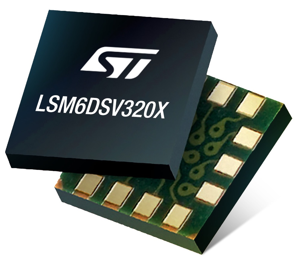
One misconception we often encounter is that Rust is inherently “faster” than C or C++. The truth is far more nuanced. Depending on the application, Rust may be slower than, on par with, or faster than C. However, in many instances, Rust forces teams to rewrite their application, which naturally leads to refactoring, dropping legacy code, or creating new, optimised processes. The absence of a garbage collector in Rust, or its modern compiler enhancements, certainly helps, but embedded system developers should not rush in thinking it will magically provide significant runtime improvements. However, it will offer significantly safer, often more flexible code, which is why we are providing Rust alternatives for our C sensor drivers.
Reason Three: The Rust CommunityThe discussions in our GitHub repository for this project show a thriving community, which is an important factor for many developers. It’s not just key industry players like Meta, Google, or Microsoft that have publicly pledged to adopt the new programming language. Many smaller teams are investing in the new language because acquiring fluency takes time, and falling behind could lead to significant technical debt that would benefit a competitor. We know that adoption is still in the early phase. This is why we are providing Rust sensor drivers now. ST wants to support those who want to be first in this transition, which seems to be shaping the future of embedded systems development.
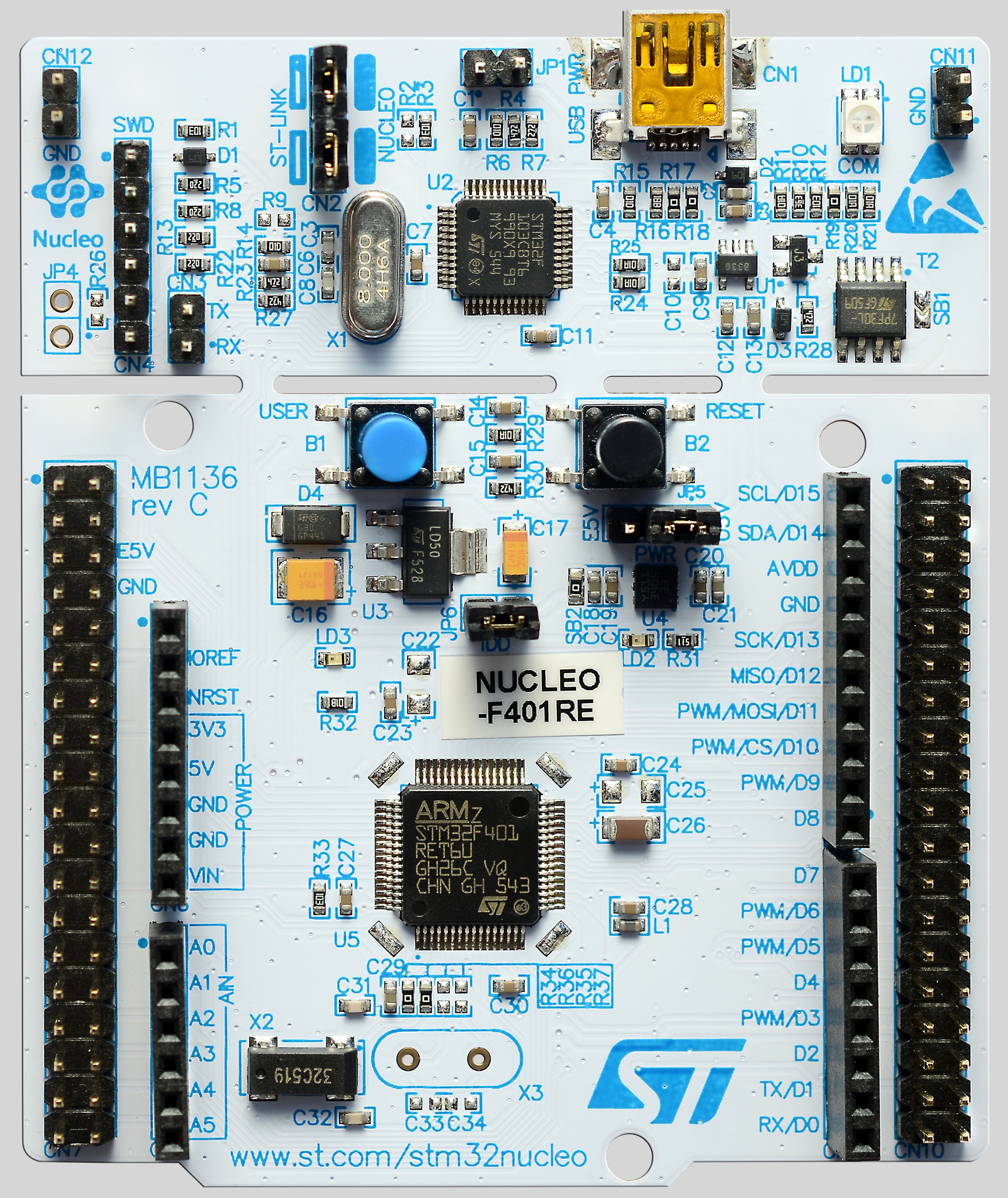
The best way to get started is to install Rust using rustup, then, as developers build their project, grab one of our packages on Crates. Our GitHub Page also walks users through the download and integration process. We offer examples in Cargo to help teams get results faster. And while the drivers themselves allow engineers to be MCU-agnostic, the examples we use are written for STM32 microcontrollers and primarily use the NUCLEO-F401RE development board. Current Rust drivers focus on I2C and SPI interfaces, as these are by far the most commonly used, but additional support, including I3C, is underway, and we will update this blog post as we release major updates.
The post Rust MEMS Drivers: 3 Reasons to Try and Adopt Our New Sensor Drivers Written in Rust appeared first on ELE Times.
I like tight pads and I cannot lie
 | submitted by /u/m4rkw [link] [comments] |
Technological roadmap proposed for lifetime brain-wide neural recordings
The Microsoft-reminiscent iPhone Duo: How much customer holding-and-folding is necessary to keep Apple from folding on the experiment?

New smart phones, earbuds and watches, this year with an added dash of memory price increases. It’s September in Cupertino again.
September 1 was Tim Cook’s last day as Apple’s CEO, after a 15-year tenure with that title. Hereafter he’ll be Executive Chairman of the board of directors, succeeded as CEO by John Ternus, former senior vice president of Hardware Engineering. And reflective of the changing of the guard, Cook was nowhere to be seen in this morning’s prerecorded launch event video, albeit in a brief cameo at the beginning.
Not because, I suspect, Cook’s got anything against product launches, although after having fronted so many of them by now, he’d certainly be entitled to a bit of burnout. Instead, I’m guessing he just wanted to make the passing of the baton as clean and obvious as possible.
Just like last year…and the year before it…and…Apple launched new and updated wearable and broader mobile products in September 2026 (which, I’ll note, has just started, so we might not be done with the month yet, far from the rest of the year). The biggest surprise this time around was that today’s unveilings weren’t the first in this year’s late-summer sequence, having been preceded by the release of new M-series SoCs and systems containing them late last month.
And speaking of M-series SoCs, there’s as-usual no shortage of commonality between those earlier latest-generation application processors for computers and high-end tablets and the one(s?) that rolled out today for high-end iPhones. Speaking of which…
The iPhone 18 Pro series
What do you do if rising DRAM and flash memory costs are clobbering your products’ bill-of-materials budgets? You focus your new-product energy on the stuff that’s most profitable already. And you do something else…which I’ll share in a minute. New stuff first. There’s no mainstream iPhone 18 yet, for the first time ever. But the high-end iPhone 18 Pro and Pro Max are here. And they’re priced $100 higher than were their forebears of similar memory capacities, along with adding an even higher-end (and higher-priced) 2 Tbyte storage tier.
That new SoC? It’s the A20 Pro. First-time 2 nm-fabricated by foundry partner TSMC. 50% higher memory bandwidth than the A19 Pro. Faster CPU (6 cores total, 2 “super” and 4 “efficiency) and GPU (seven cores total) subsystems than those in the A19 Pro. And a dual 16-core Neural Engine inference subsystem. Lessee…where have we heard this same messaging…two weeks ago, to be exact? Yessiree, it seems that once again there’s no shortage of shared DNA between the late-August M6 and today’s A20 Pro SoCs, albeit with varying dollops of various on-die resources, befitting varying platform cost, feature and performance requirements.
What I’m admittedly most excited about as an unabashed photography geek is the camera subsystem’s variable aperture (along with, by association, manual shutter speed setting) support for the rear main unit.
Yes, it enables more meaningful user control of exposure, particularly in low light environments (adjusting for bright-light settings can always alternatively be done via integrated or external neutral density filters, of course). But it also first-time affords user adjustment of depth of field, allowing for both shallow-depth “bokeh” effects and sharpness across a wider depth range than possible before.
Oh, and by the way…even though Apple delayed releasing the mainstream iPhone 18 (which, in saying so, I’m obviously assuming is still coming eventually), the company still found another way to use our credit cards and bank accounts as counterbalance to the higher semiconductor-content costs it was incurring. The iPhone 17 Pro and Pro Max are no more, of course. But the company’s still selling the baseline iPhone 17 and 16, the boutique iPhone Air, and the “cost-effective” (relatively speaking, at least) iPhone 17e. That said, post-Apple Store resurrection mid-day today, they all now cost $100 more than they did yesterday. Yay…???
The AirPods 5
Two years ago this same month, Apple released the 4th-generation AirPods in two flavors, $129 with only passive noise reduction (PNR, and not great, at that, given their imperfect ear-shape seal for many users), and $50 more for an active noise control (ANC)-supportive model. I’d love to see the comparative sales stat results between the two variants, but clearly the world has moved en masse to ANC since then.
To wit, Apple’s fifth-generation AirPods successors have dropped the PNR option, but the company’s marketeers can’t seem to quit the price-differentiation shtick completely. Want a conventional wired-charging case? That’ll cost you $129. How about a wireless charging-capable case option? $20 more, please. Maybe two years from now, Apple Marketing will realize that the world’s already moved en masse to Qi…oh, sorry, this is Apple…MagSafe…too. Wonder how they’ll try to extract more money out of our wallets next time? Reader prognostications are as-always welcomed in the comments!
Apple Watch Series 12 and Watch Ultra 4

Three key takeaways distinguish this year’s mainstream and high-end smartwatches from their prior years’ versions:
- An upgraded S11 processor, whose specifics were as-usual not revealed but likely include a sprinkle (or few) of deep learning inference acceleration, reflected in…
- AI as a first-time notable element in Apple’s smartwatch pitch this time, particularly focusing on ambient audio processing capabilities (including conversations, although Apple predictably maintains its “privacy by design” reassurance mantra) and thanks in no small part to a recently unveiled partnership with Google that has seemingly finally gotten Siri on track for something other than corporate embarrassment, and…
- The other notable AI-analyzed data set, an enhanced health sensor suite enabling, among other things, continues heart rate monitoring every five seconds, all day.
This year’s models are identically priced to their generational predecessors, surprisingly, although around 24 hours ago, I’d wondered if Apple was going to deal with its burgeoning semiconductor memory bill-of-materials burden in a different way. Beginning some time yesterday and continuing for quite a while, although subsequently corrected, the company’s entry-level Apple Watch SE 3 models all became “unavailable” for purchase.
Apple typically takes its online store down a few hours ahead of launch events to make the necessary tweaks in preparation and out of the public eye, but this was unprecedented. I’d wondered if Apple was planning on dropping the whole line, either because it wasn’t AI-capable and/or because memory cost increases had rendered it insufficiently profitable, and if someone had “pulled the plug” prematurely and highly visibly. But given that the Watch Series 3 had just been unveiled a year ago, the “yank” seemed premature. As, it turned out, it was. Maybe. Then again, maybe someone just decided to do a last-minute course-change. We’ll likely never know.
Back to the futureI guess John Ternus thought that instead of charting his own course, he’d use his first launch event to “channel” a predecessor’s past glory. Yes, he pulled out the memory closet a Steve Jobs “chestnut”, the “one more thing”. And of course, it was one of the worst kept secrets of recent Apple corporate strategy: the foldable iPhone. Although at least one thing was surprising about it: industry scuttlebutt had long branded it the “iPhone Ultra”, but instead it’s the “iPhone Duo”. Begging the question of what, if anything, the “iPhone Ultra” will be…but I digress.
It’s $1999 (and up, capacity-dependent). It won’t be available until next month (October). And like its iPhone 19 Pro siblings, it’s based on the A20 Pro Soc. But I don’t want to spend my precious few remaining paragraphs in this section talking about that. Instead, I want to talk about aspect ratios. Let’s start with my long beloved, in spite of chronic software bugs, Microsoft Surface Duo, an example of which still inhabits my storage closet in the hopes that someone will someday release a stable, robust-featured, reasonably current Android build for it or…dare I dream…Windows 11 for Arm with Wi-Fi and cellular data support? Be still my heart.
Yes, it was foldable. But no, unlike the iPhone Fold it wasn’t comprised of a single piece of bendable OLED internal “glass”. Instead, there was that jarring hinge in-between the two internal displays. And there was no external screen, either, so you had to unfold it to use it at all, even for basic smartphone tasks. But again, I digress. Look at its aspect ratio. Unfold it and, without rotating it 90°, you had a 7.36” wide by 5.72” tall screen (yes, I know, with a gap in the middle) perfect for reading eBooks in a style akin to that of actual books, watching movies, and the like.
Next, let’s look at the first-generation (2023) Google Pixel Fold, an example of which my wife bought me for my birthday earlier this year.

Same fundamental aspect ratio, this time with an added bonus: no midway gap. And this time, there was a third outer display, too.

But given overall system form factor dimensions, it was atypical in both size (5.8” diagonal) and (especially) aspect ratio in comparison to the ones in conventional smartphones. Atypical equals low volume. Low volume equals costly and supplier-option deficiency. All of which explains why second and subsequent-generation Pixel Folds have switched to “bifolds”, taller than before, albeit losing the unfolded “book” (or, if you prefer, movie screen) form factor in the process.


Now look at the iPhone Fold again. The “book” form factor is back (in black, aka “night sky”, as well as “star white”)!

Apple perhaps obviously has supplier leverage that Google doesn’t (or at least didn’t) have, so assuming customers buy into the design decision, I suspect it’ll play out better this time around. Agree or disagree, readers? Let me know your thoughts on this or anything else I’ve discussed here, in the comments!
—Brian Dipert is the associate editor, as well as a contributing editor, at EDN.
Related Content
- Apple’s processor cadence: A pending stutter-step for improved long-term edge inference?
- Apple’s question for the developer: Are you up for an AI do-over?
- Apple’s 2H 2025 announcements: Tariff-touched but not bound, at least for this round
- Microsoft’s Surface Duo: A software evolution testimonial, but for who?
The post The Microsoft-reminiscent iPhone Duo: How much customer holding-and-folding is necessary to keep Apple from folding on the experiment? appeared first on EDN.
DB HiTek completes reliability qualification for 8-inch 1200V SiC MOSFET process
Сторінки




![[link]](https://i.redd.it/h9mszij28qoh1.png)
![[link]](https://i.redd.it/72buocm0anoh1.jpeg)