
Збирач потоків
GaN transistor cuts losses and heat

EPC’s first Gen 7 eGaN power transistor, the 40-V EPC2366, delivers up to 3× better performance than equivalent silicon MOSFETs. Now entering mass production, the device features a typical RDS(ON) of 0.84 mΩ and an optimized RDS(ON) × QG figure of merit of 12.6 mΩ·nC. This enables the EPC2366 to reduce conduction and switching losses while improving thermal performance.

Designed for high-efficiency, high-density power systems, the EPC2366 is suitable for synchronous rectifiers, DC/DC converters, AI server power supplies, and motor drives. It is rated for a drain-to-source voltage (VDS) up to 40 V, transient voltages up to 48 V, and a continuous drain current (ID) of 88 A, with pulsed currents reaching 360 A.
To assist design-in and evaluation, the EPC90167 half-bridge development board integrates two EPC2366 transistors in a low-parasitic layout, with PWM drive signals and flexible input modes.
The EPC2366 comes in a compact 3.3×2.6-mm PQFN package and is priced at $1.56 each in quantities of 3000 units. The EPC90167 development board is available for $211.65 each.
The post GaN transistor cuts losses and heat appeared first on EDN.
High-density power module fits compact AI servers

Enabling higher power delivery within the same rack space, Microchip’s MCPF1525 power module delivers up to 25 A per device and can be stacked to 200 A. The module integrates a 16-VIN buck converter with programmable PMBus and I²C control, making it well suited for powering PCIe switches and high-compute MPU applications used in AI deployments.

With dimensions of approximately 6.8×7.65×3.82 mm, the MCPF1525’s vertical construction maximizes board space, providing up to a 40% reduction in board area compared to alternative solutions. For improved reliability, the device incorporates multiple diagnostic functions reported over PMBus, including overtemperature, overcurrent, and overvoltage protection to help prevent undetected faults.
Housed in a thermally enhanced package, the MCPF1525 supports a junction temperature range from −40°C to +125°C. An embedded EEPROM enables users to program the default power-up configuration.
The MCPF1525 is available now, priced at $12 each in 1000-unit quantities.
The post High-density power module fits compact AI servers appeared first on EDN.
Vishay shrinks inductors, keeps full performance

Four power inductors in 0806 and 1210 case sizes from Vishay offer improved performance for commercial and automotive applications. Compared to competing inductors with similar performance, the devices use considerably less board space—up to 64% smaller in 0806 and 11% smaller in 1210 packages. They also support higher operating temperatures, a wider range of inductance values, and lower DC resistance to enhance efficiency.

The commercial IHLL-0806AZ-1Z and IHLL-1210AB-1Z have terminals plated only on the bottom, enabling smaller land patterns for more compact board spacing. The automotive-grade IHLP-0806AB-5A and IHLP-1210ABEZ-5A feature terminals plated on the bottom and sides, allowing a solder fillet that strengthens the mount against mechanical shock and simplifies joint inspection. These automotive devices are AEC-Q200 qualified for high reliability and elevated operating temperatures.

Samples and production quantities of the IHLL-0806AZ-1Z, IHLL-1210AB-1Z, IHLP-0806AB-5A, and IHLP-1210ABEZ-5A inductors are available now, with lead times of 10 weeks.
The post Vishay shrinks inductors, keeps full performance appeared first on EDN.
NUBURU accelerates defense & security platform execution while advancing balance sheet transformation and multi-vertical technology integration
[OC] Successful Hashboard Rework; S21 Pro A3HB70601
![[OC] Successful Hashboard Rework; S21 Pro A3HB70601](https://a.thumbs.redditmedia.com/F_zkbqiw7CibiGOOF1un3k7ctd1TTk7hz5XHVlaWv34.jpg "[OC] Successful Hashboard Rework; S21 Pro A3HB70601") | S21Pro, successful rework and trace repair. AMA! ( Ps: Sorry about the double post; I wanted to be more detailed than my prior post because this community is more receptive than the soldering subreddit. Also, I am fully self taught on everything here, so pardon my ignorances on some terminology. Not IPC certified either. — — — ) The goal of this repair is to achieve a successful count of all 65x asics on this PCB. Image 2 shows a fail on full count. Image 12 shows a successful fix. Image 1, shows my main circuit with issues, conformal coating still present. Arrows and circles identifying components I eventually replaced, or repaired. Darker spots on the conformal coating indicates that these circuits overheated and likely shorted out. Image 2, shows the entire single layered PCB, plus includes the readout from my ASIC tester (it’s called a Stasic.). Started removing conformal coat. Image 3, closeup of problem circuit with conformal coating removed. Burnt diode from my boost circuit and clear signs of shorts throughout several dependent circuits. Image 4, propane blowtorch used to reflow the first half of my boost circuit. ( I imagine this photo is what will cause some concern. This is a method I’ve used thousands of times at this point. While it works, it is not my sole methodology for reflow. Also, I offer warranty on my repairs. ) Image 5, closeup of first ASIC removed. My two main vdd signals would not pass this chip. Removal helped identify those corroded pads, and prompted me to remove, and check other asics in the physical area. Images 6 and 7, closeup of the previously corroded pads on the asic chip; cleaned and ready for tin. Next was the hard part. Image 8, closeup tinned asic. Passed continuity test, despite the ugly-lumpy pads. Image 9 and 10, closeup of the original pads where my first corroded asic was removed; and closeup of it after being tinned. Image 11, previously corroded PCB and ASIC chip repaired, and successfully placed. (( Just throwing it out there that I placed this asic with the blowtorch lol. )) Images 12, 13, and 14 (12 & 14 unlabeled), closeup of the entire area fixed. Another angle of the chip placed (that bridge is intentional; bypassing a 1k resistor), and the reveal that the entire back-half of this board is solid aluminum. [link] [comments] |
you can have your resistors, I'll sort my transistors...
Just like the resistor guy, I could not resist, because I've got a bad conscience like he did, and I have this drawer full of transistors for 20+ years, one day...
[link] [comments]
Ascent Solar developing CIGS PV modules generating multiple times more power for space beaming
Skyworks’ continuing revenue growth in Broad Markets counteracts seasonal decline in Mobile
Added-conductor and directional audio interconnects: Real-life benefits?

Does vendor-claimed audio cable directionality make theoretical sense, far from delivering real-life perceptible benefit? And what about the number and organization of in-cable conductors?
Within my recently published two-part series on the equipment comprising my newly upgraded home office audio setup, I intentionally left out one key piece of the puzzle: the cables that interconnect the various pieces of gear in each “stack”. Come to think of it, I also didn’t mention the speaker wire that mates each monoblock power amplifier to its companion speaker:

but that’s a hype-vs-reality quagmire all its own! Maybe someday…for now, I’ll tease you with the brief revelation that it’s a 2m (3.3 foot) GearIT 14 AWG banana-plug-based set purchased in like-new condition from Amazon’s Resale (Warehouse) section for $17.18:

Back to today’s quagmire  When spanning the equipment placed on consecutive shelves of each audio “stack”, the 6” cable length is ideal. For the balanced interconnect-based setup located to my left on my desk:

wherein all of the connectors are XLR in form factor, I’ve found Coluber’s cables, available in a variety of connection-differentiating colors as well as as-needed longer lengths, to be excellent:

This particular setup, now based on a Drop + Grace Design SDAC Balanced DAC:


initially instead used Topping’s D10 Balanced DAC:

whose analog line-out connections were ¼” TRSs, not XLRs:

In that earlier gear configuration, I’d relied on a set of WJSTN Suanqi TRS-to-XLR cables to tether the DAC to the headphone amp (the Schiit Lokius equalizer wasn’t yet in the picture, either):

What about the unbalanced (i.e., single-ended) interconnection-based setup to my right?

In this case, I’ve mixed-and-matched RCA-to-RCA cables from WJSTN:

and equally highly-rated CNCESS:

depending on whose were lower-priced at any particular purchase point in time.
A pricier (albeit discounted) experimentSpeaking of economic factors, as regular readers may recall from past case studies (not to mention my allusion by example earlier in this writeup), I regularly troll Amazon’s Resale (formerly Warehouse) site for bargains. Last summer, I came across a set of “acceptable” condition (i.e., packaging-deficient) 0.5-foot-long RCA cables from a company called (believe it or not) “World’s Best Cables”:

and titled as follows:
0.5 Foot RCA Cable Pair – WBC-PRO-Quad Ultra-Silent, Ultra-Flexible, Star-Quad Audiophile & Pro-Grade Audio Interconnect Cable with Amphenol ACPR Gold RCA Plugs – Gray & Red Jacket – Directional
Say that ten times real fast, and without pausing to catch a breath midway through!
They normally sell for $30.99 a pair on the company’s Amazon storefront, which is pretty “salty” considering that the CNCESS and WJSTN alternatives are a third that amount ($10.99 for two). That said, these were discounted to $18.82, nearly half off the original price tag. I took the bait.

Like I said earlier, “packaging-deficient”.
How’d they sound? Fine. But no different, at least in my setup and to my ears, than the brand new but still notably less expensive CNCESS and WJSTN ones. This was the case in spite of the fact that among other things they were claimed to be “directional”, the concluding word in the voluminous product title and the one that had caught my ever-curious eye in the first place.
Directional detailsAs I’ve groused about plenty of times in the past, the audio world is rife with “snake oil” claims of products and techniques that supposedly improve sound quality but in actuality only succeed in extracting excess cash from naïve enthusiasts’ wallets and bank accounts. My longstanding favorite snake-oil theory, albeit one that mostly only wasted adoptees’ time, was that applying a green magic marker to the edges of an optical audio disc would improve its sound by reducing laser reflections.
Further magnifying this madness, at resultant higher damage- therefore wallet-induced devotee expense, was the practice of beveling (i.e. shaving down) those same edges:
I’ve also come across plenty of cables, both signal and power, and in various shapes and sizes, that claim to benefit from directionality induced by their implementations. Such directionality is, of course, forced on the implementation by USB cables, for example, which (for example, redux) have a Type A connector on one end for tethering to a computer and a Type B connector on the other end for mating with, say, a printer. Both types are shown at right in the following photo:

Conceptually, the same thing occurs with power cords, of course, such as this one:

But that’s not what I’m referring to. I’m talking about claimed directionality introduced within the cable itself—by the materials used to construct it, the conductors within it, etc. For cables that carry digital signals, this is pure hogwash as far as I can tell. But for analog cables like the one I’m showcasing today? There may, it turns out, be some reality behind the hype, depending on what kind of signal the cable’s carrying and for what span length, along with the ambient EMI characteristics of the operating environment. Quoting from the Amazon product page:
Each cable is configured as a “Directional” cable and as such the shield of the cable is connected to the ground only at the signal emitting end. This allows the shield of the cable to work as a Faraday’s cage which rejects external noise that could degrade the signal. The cable will work even if you plug it the opposite direction, but this will diminish the noise rejection capabilities of the directional design. This enhances the noise rejection capabilities of our cables over our competition.
To clarify: when I said earlier that I discerned no difference in the sound between the “World’s Best Cables” interconnect and its more cost-effective alternatives, I was referring to:
- Short cable spans (6”) transporting
- Reasonably high-level innate signals (specifically line level, 0.3V to 1.2V)
Would an alternative RCA cable set carrying, for example, the lower magnitude output signal of a turntable cartridge—moving magnet (3-7 mV) and especially moving coil (0.2-0.6 mV)—to a phono preamp be more prone to the corrupting effects of environmentally induced noise, especially in high EMI (with an overlapping spectral profile, to be precise) environments and across long cable runs? Low-level microphone outputs are another example. And would shielding—especially if directional in its nature—be of benefit in such scenarios?
Twist, double up and fan outTruth be told, I’d originally planned to stop at this point and turn those questions over to you for your thoughts (both on them specifically and on the topic more generally) in the comments. But in looking again at the conceptual cable construction diagram this morning while prepping to dive into writing:

I noticed not only the shielding, which I’d seen before, but that there were four conductors within it. Each RCA connector is normally associated with only two wires, corresponding to the positive and negative per-channel connections to the audio source and destination devices.
 Version 1.0.0
Four total wires might make sense, for example, if we were looking at the middle of a unified cable, with both channels’ dual conductors combined within a common shield. And it might also make sense (albeit seemingly still with one spare wire) if the per-channel cable connections were balanced. But these are RCA cables: unbalanced, i.e. single-ended, and only one cable per channel. So why four connectors inside, instead of just two?
My first clue as to the answer came when I then looked at the top of this graphic (table, to be precise):

Followed by my noticing the words “WBC-PRO-Quad” and “Star-Quad” in the aforementioned wordy product title. My subsequent research suggests that the term “Star Quad” isn’t unique to “World’s Best Cables”, although it typically refers to mic and other balanced interconnect applications:
The star quad design is a unique configuration of wires used in microphone cables. Unlike traditional cables that consist of two conductors, the star quad design incorporates four conductors. These conductors are twisted together in a specific pattern, resembling a star shape, hence the name. The layout of the conductors in a star quad cable significantly reduces electromagnetic interference (EMI), resulting in cleaner and more reliable audio transmission.
And how do two connections at each cable end translate into four conductors within the cable?
Star-quad microphone cables are specially designed to provide immunity to magnetic fields. These microphone cables have 4 conductors arranged in a precise geometry that provides immunity to the magnetic fields which easily pass through the outer RF shield. Four conductors are arranged in a four pointed star configuration and the wires at opposite points of the star are connected together at each end of the cable.

When the cables are wired in this manner, the + and – legs of the balanced connection each receive equal induced voltages from any magnetic field. This configuration balances the interference to the + and – legs of the balanced connection. The key to the success of star-quad cable is the fact that the magnetically-induced interference is exactly the same on the + and – legs of the balanced connection. The star-quad geometry of the cable keeps the interference signal identical on both legs no matter what direction the magnetic interference is coming from.
In the “a picture paints a thousand words” spirit, this additional graphic might be of assistance:

Along with this lab equipment- and measurement-flush video:
But again, we’re still talking about long-length, low-level balanced cables and connections used in high-EMI operating environments. How, if at all, do these results translate to the few-inch, comparatively high-level and low-EMI applications that my “World’s Best Cables” target, especially considering that they also include heavily hyped directional shielding? Even audiophiles have mixed opinions on the topic.
And so, at this point, after twice as long a write-up as originally planned, I will now stop and turn these and my prior questions over to you for your thoughts (both on them specifically and on the topic more generally) in the comments!
—Brian Dipert is the Principal at Sierra Media and a former technical editor at EDN Magazine, where he still regularly contributes as a freelancer.
Related Content
- Sonic excellence: Music (and other audio sources) in the office, part 1
- Sonic excellence: Music (and other audio sources) in the office, part 2
- Peeking inside a moving magnet phono cartridge and stylii
- Microphones: An abundance of options for capturing tones
The post Added-conductor and directional audio interconnects: Real-life benefits? appeared first on EDN.
КПІшники на технологічній виставці CES у Лас-Вегасі

🤩 12 студентів КПІ — серед 29 українських студентів технічних спеціальностей — відвідали Consumer Electronics Show (CES) 2026 у Лас-Вегасі (США), одну з наймасштабніших світових виставок споживчих технологій.
📢 Запрошуємо до участі у X Міжнародній Самсонівській конференціі “Materials Science of Refractory Compounds” (MSRC-2026)

Шановні колеги! 📢 Запрошуємо до участі! 25 - 28 травня 2026 року в Києві відбудеться X Міжнародна Самсонівська конференція імені Г. В. Самсонова “Materials Science of Refractory Compounds” (MSRC-2026)
Silicon Shield: Role of Semiconductors in Modern Warfare
Courtesy: Orbit & Skyline
War has always been part of human history, and true global peace still seems far away. While modern wars may look intense on TV screens, they are generally far less deadly and destructive than what the world has seen in the past. For example, in February 1945, during the bombing of Dresden, Germany, Allied planes dropped unguided bombs aimed at disrupting supply lines. However, the attack triggered a firestorm that killed about 25,000 people and destroyed most of the city, even though it wasn’t a major military target. In contrast, recent conflicts around the world have used far more advanced weapons but resulted in fewer casualties. As military technology evolved from gunpowder to tanks to nuclear weapons, wars became shorter, though still devastating. World War-2 remains the deadliest, with an estimated 70–80 million lives lost.
Today, most battles are fought remotely using advanced weapons that strike deep into enemy territory while keeping one’s own forces out of harm’s way. Modern air battles are fought primarily in the Beyond Visual Range (BVR) domain. The era of vintage fighter planes engaging in close-range dogfights is long gone. Today’s fighter jets are equipped with missiles capable of striking targets nearly 200 km away, far beyond visual sight. To detect and track such distant targets, they rely on advanced AESA (Active Electronically Scanned Array) radars and are supported by airborne AEW&C (Airborne Early Warning and Control) systems that serve as eyes in the sky. These BVR engagements are made possible by sophisticated electronic systems, sensors, and radars, all of which depend on complex semiconductor technologies to enable their advanced capabilities.
The shift in battlefield tactics has reduced civilian harm and damage. This is mainly due to precise, guided weapons powered by semiconductor-based integrated circuits (ICs) that enable smart targeting and real-time tracking. Semiconductors, which revolutionised smartphones and satellites, have also made weapons smarter, faster, and more accurate. These ICs are key to guided missiles, radars, drones, and surveillance systems, processing huge amounts of data quickly for precise targeting, adaptive routes, and secure communication. Such electronics have moved warfare from blunt attacks to focused, strategic strikes.
Rise of Precision Warfare
Warfare has significantly transformed from the close-combat battles of the past to today’s reliance on unmanned systems like missiles and drones. A century ago, weapons such as tanks, rifles, and grenades, primarily mechanical and chemical systems, were designed for maximum destruction, often resulting in heavy casualties with little concern for collateral damage. Modern armies no longer use inaccurate, unguided weapons that can cause accidental damage and political problems, especially with the world watching closely. Such mistakes can harm their goals.
Today, nations prioritise precision and control in military operations through smart, guided weapons. These rely on semiconductor components for navigation, guidance, surveillance, and reconnaissance, enhancing effectiveness and enabling shorter, more focused missions. Precision weapons allow defence forces to deliver targeted strikes with minimal collateral damage, signalling intent without triggering full-scale conflict. This strategy provides several key advantages:
- Targeted Messaging: Precision strikes focus on military assets, deterring adversaries without full-scale war.
- Escalation Control: Pinpoint accuracy neutralises threats efficiently, avoiding prolonged conflicts.
- Reduced Civilian Casualties: Minimal unintended damage preserves legitimacy and prevents escalation.
- Strategic Deterrence: Precise attacks discourage aggression by keeping critical assets vulnerable.
Semiconductor Technologies in Advanced Weapon Systems
Semiconductor technologies are essential in modern weapon systems, enhancing precision, range, guidance, navigation, surveillance, and electronic warfare. Here are some examples of how various semiconductor technologies (Silicon, GaN, MEMS, FPGAs, Sensors, etc.) are used in modern weapon systems:

Electronics warfare and Radar: Electronic warfare (EW) and radar systems, built on different semiconductor technologies, form the key driver of battlefield dominance. Integrated circuits (ICs) fabricated using technologies such as CMOS, GaN, GaAs, and SiGe enable operation across low-frequency digital domains and high-frequency bands—from L-band to millimetre-wave. These technologies support critical functions like signal detection, response generation, and countermeasures, enabling fast RF transmission, real-time processing, and agile control essential for modern EW and radar systems.
At the front end, GaN-based high electron mobility transistors (HEMTs) in monolithic microwave integrated circuits (MMICs) deliver high-power RF amplification with good thermal efficiency, key for long-range radar and jamming. These are paired with low-noise amplifiers (LNAs), often made using SiGe BiCMOS or pHEMT processes, to ensure high sensitivity and signal integrity. RF switches and phase shifters, built on SOI or RF MEMS, enable dynamic beam steering in AESA radars, allowing electronic scanning without moving parts.
High-speed analogue-to-digital (ADC) and digital-to-analogue converters (DAC), typically CMOS or bipolar, digitise wideband signals for baseband processing. Radiation-hardened FPGAs and DSP cores handle FFTs, beamforming, and adaptive filtering. PLL synthesisers and VCOs, using SiGe or advanced CMOS, provide low-jitter, frequency-agile clocking critical for threat detection and deception. Together, these semiconductor components form the backbone of radar and EW systems, delivering precision, speed, and resilience in modern electromagnetic warfare.
Guidance and Navigation: In modern missiles and drones, guidance and navigation rely heavily on semiconductor-based components that ensure precision and reliability even in challenging environments. At the core of these systems are inertial navigation systems (INS), which use MEMS accelerometers and gyroscopes to measure motion and orientation without external signals, crucial for operation in GPS-denied conditions. These are often integrated into compact IMUs (Inertial Measurement Units) that fuse data in real time to calculate position and velocity. When GPS signals are available, GNSS receiver chips provide absolute positioning by processing satellite signals, with advanced modules incorporating anti-jamming and anti-spoofing features to maintain accuracy under electronic warfare. Complementing these are digital signal processors (DSPs) and microcontrollers (MCUs), which handle sensor data processing, flight control algorithms, and real-time decision-making. These systems typically utilise semiconductor technologies such as CMOS for GNSS and signal processing ICs, MEMS processes for inertial sensors, and advanced packaging to integrate these functions in compact, rugged modules. Together, these semiconductor components enable autonomous, accurate, and adaptive navigation critical to modern missile and UAV operations.
Explore how we at Orbit & Skyline help global FABs and system integrators by supporting GaN process optimisation, enabling better RF and radar performance. Read our related post on GaN in semiconductors here.
Surveillance and Reconnaissance: Surveillance and reconnaissance systems today use many types of semiconductor technologies for sensing, data processing, and secure communication. CMOS and CCD image sensors are used in electro-optical and night vision equipment. For thermal and FLIR imaging, infrared detectors made from materials like InGaAs, HgCdTe, and InSb are combined with special Readout ICs (ROICs). In radar systems, GaN HEMT chips are used in power amplifiers to send signals efficiently, while SiGe or pHEMT-based LNAs help in receiving weak signals clearly.
High-speed ADCs and DACs made using CMOS or BiCMOS are used to convert radar signals, including those from Synthetic Aperture Radar (SAR), into digital form for further analysis. SAR provides clear images even at night or in bad weather. Systems use FPGAs, SoCs, and AI chips, often made with advanced FinFET technology, to process this data quickly. AI edge ICs make fast, low-power decisions on the spot. DRAM and SRAM store sensor data, while secure MCUs and RF transceivers enable encrypted, high-speed communication. Together, these semiconductor parts help satellites, aircraft, and drones deliver accurate, real-time battlefield information.
Tiny Chips, Big Defence
Semiconductors also serve as a shield for nations, not just for those using advanced weapons, but especially for those that develop them. While many countries can buy defence systems, only a few can design and manufacture the complex semiconductor ICs inside them. These ICs are classified as commercial, military, or space-grade, with increasing reliability and performance demands. Military systems often operate in extreme conditions from -40°C to 150°C, requiring robust, fail-proof chips. Access to such military-grade ICs is restricted by various regulations and export controls. Hence, having a domestic, secure semiconductor manufacturing ecosystem is critical. Without it, countries risk supply-chain disruptions during strategic needs. These ICs function as sensory organs; eyes, ears, and brains of missiles, drones, and UAVs, and are essential for mission success.
A nation with precision-strike capabilities can deter adversaries from engaging in prolonged conflict, something seen very clearly in recent global conflicts. These semiconductor-driven systems form a “Silicon Shield,” reducing the impact of warfare on civilians and infrastructure. Compared to the devastation of the World Wars, recent conflicts have seen far less destruction, underlining the value of precision weapons in enabling restrained and strategic military actions.
The post Silicon Shield: Role of Semiconductors in Modern Warfare appeared first on ELE Times.
Андрій Макарчук: "Всебічна комунікація завжди приносить результат"

Наприкінці минулого року вийшов наказ МОН про призначення академічних стипендій Президента України аспірантам на 2025/2026 навчальний рік. Її отримають здобувачі, які мають видатні наукові чи навчальні досягнення, як заохочення їхньої діяльності та мотивацію до високих результатів. Серед нагороджених і Андрій Макарчук, асистент кафедри інженерії програмного забезпечення в енергетиці НН ІАТЕ.
Silicon Photonics: The Lightspeed Revolution That Will Transform AI Computing
Courtesy: Lam Research
Lam Research is setting the agenda for the wafer fabrication equipment industry’s approach to a silicon photonics revolution, driving the breakthroughs in Speciality Technologies that will enable sustainable AI scaling through precision optical manufacturing.
The artificial intelligence boom has created an energy crisis that threatens to consume more electricity than entire nations. As data centres race to keep pace with AI’s insatiable appetite for computational power, technology leaders like Lam are shaping a fundamental shift that could redefine how we think about high-performance computing. One solution lies in replacing the electrical interconnects that have powered computing for decades with something far more efficient: light.
AI’s Energy Crisis: Why Power Demand Is Surging in Data Centres
Goldman Sachs projects a 160% increase in data centre power demand by 2030, reaching 945 terawatt-hours annually — equivalent to Japan’s entire electricity consumption.
The problem runs deeper than software inefficiency. According to Bloomberg, AI training facilities house hundreds of thousands of NVIDIA H100 chips, each drawing 700 watts, nearly eight times the power consumption of a large TV. Combined with cooling systems, some hyperscale facilities now require as much power as 30,000 homes, driving tech companies to seriously consider dedicated nuclear plants.
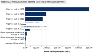 Source: Nvidia. Apart from average estimates, power data for racks are based on Nvidia specifications. 2025 and later are estimates. AI server racks refer to GPU racks. General-purpose racks refer to CPUs.
The Paradigm Shift
Meeting this challenge requires a fundamental change in how chips are designed and connected. Silicon photonics—using light to transmit data—has the potential to provide dramatic improvements in speed and efficiency over traditional electrical interconnects. Precision optical manufacturing makes this shift possible, enabling scalable processes that can support the next era of energy-efficient, high-performance computing.
Silicon photonics represents a fundamental reimagining of how data moves within computing systems. Instead of pushing electrons through copper wires, this technology uses photons—particles of light—to carry information through silicon waveguides that function like nanoscale fibre optic cables, integrated directly onto chips.
The efficiency gains are dramatic. Optical interconnects consume just 0.05 to 0.2 picojoules per bit of data transmitted, compared to the much higher energy requirements of electrical interconnects over similar distances. As transmission distances increase, even within a single package, the energy advantage of photonics becomes overwhelming.
TSMC has published several research papers on silicon photonics since late 2023. The company has announced public partnerships with NVIDIA to integrate optical interconnect architectures into next-generation AI computing products. Lam is leading the industry’s approach to the transition to silicon photonics. As a technology leader with deep expertise in precision manufacturing, we are defining the roadmap for silicon photonics production, working closely with leading foundries and fabless companies to address the unique challenges presented by optical interconnects.
According to Yole Group, the market for silicon photonics is expected to grow from $95 million in 2023 to more than $863 million in 2029, with a 45% annual growth rate that reflects the technology’s expected rapid commercial adoption.
The Limits of Copper: Why Traditional Interconnects Can’t Scale With AI
At the heart of this energy crisis lies a fundamental bottleneck that has been building for years. While computing performance has advanced at breakneck speed, the infrastructure connecting these powerful processors has not kept pace. Hardware floating-point operations (FLOPS) have improved 60,000-fold over the past two decades, but DRAM bandwidth has increased only 100-fold, and interconnect bandwidth just 30-fold over the same period.
This creates what engineers call the “memory wall,” a constraint where data cannot move between processors and memory fast enough to fully use the available computing power. In AI applications, where massive datasets must flow seamlessly between graphics processors, high-bandwidth memory, and other components, these interconnect limitations become critical performance bottlenecks.
The solution that worked for previous generations—simply shrinking copper interconnects and packing them more densely—is reaching physical limits. As these copper traces become smaller and more numerous, they consume more power, generate more heat, and introduce signal integrity issues that become increasingly difficult to manage. Each voltage conversion in a data centre’s power delivery system introduces inefficiencies, and copper interconnects compound these losses throughout the system.
Modern AI architectures require what engineers call “high access speeds within the stack.” Chips become thinner, interconnects evolve from through-silicon vias (TSVs) to hybrid bonding, and memory modules must connect directly to graphics processors at unprecedented speeds. But when that high-speed memory connection has to traverse copper tracks on a circuit board to reach another processor, much of the bandwidth advantage disappears.
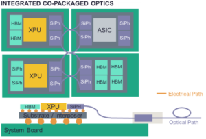
Silicon Photonics Meets AI: Co-Packaged Optics for Next-Gen Performance
Silicon photonics is not entirely new; it has powered telecommunications networks for years through pluggable transceivers that connect data centre racks. These proven systems use silicon photonic dies combined with separate lasers and micro-lens technologies packaged into modules that can be easily replaced if they fail.
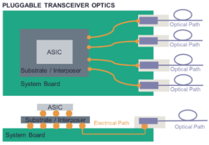
But AI’s demands are pushing photonics into uncharted territory. Instead of simply connecting separate systems, the technology must now integrate directly with processors, memory, and other components in what engineers call “co-packaged optics.” This approach promises to bring optical interconnects closer to the actual computation, maximising bandwidth while minimising energy consumption.
The challenge is reliability. While pluggable transceivers can be easily swapped out if they fail, co-packaged optical systems integrate directly with expensive graphics processors and high-bandwidth memory, making them a more reliable option. If an optical component fails in such a system, the repair becomes exponentially more complex and costly. Early implementations from major chip developers are still in pilot phases, carefully assessing long-term reliability before full-scale deployment.
Accelerating Adoption: How Industry Timelines Are Moving Faster Than Expected
Industry roadmaps that once projected capabilities for 2035 are already being met by leading manufacturers. The combination of urgent market need, massive investment, and three decades of accumulated photonics research has created what amounts to a perfect storm for commercialisation.
The implications extend far beyond data centres. As optical interconnects become more cost-effective and established, they have the potential to revolutionise everything from autonomous vehicles to edge computing devices. The same technology that enables sustainable AI scaling could ultimately transform how electronic systems communicate across virtually every application.
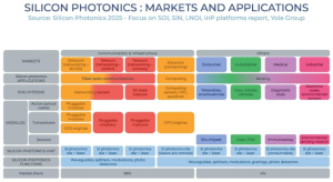 Source: Yole Group
The Future of Computing Is Optical Interconnects for Sustainable AI Growth
The question is how quickly it can be implemented and scaled. With leading manufacturers already investing billions and pilot systems entering data centres, the light-speed future of computing is no longer a distant possibility. Companies like Lam, through our customer-centric approach and advanced manufacturing solutions, enable this transformation by providing the precision tools that make commercial silicon photonics possible.
Silicon photonics represents a fundamental technology shift that could determine which companies lead the next phase of the digital revolution. Just as the introduction of copper interconnects enabled previous generations of performance scaling, optical interconnects have the potential to break through the barriers that threaten to constrain AI development.
For an industry grappling with the sustainability challenges of exponential AI growth, silicon photonics offers a path forward that doesn’t require choosing between performance and environmental responsibility. By replacing electrical inefficiency with optical precision, this technology could enable the continued advancement of AI while dramatically reducing its environmental footprint.
The revolution is just beginning, but one thing is clear: the future of high-performance computing is increasingly bright, and Lam is at the centre of it.
The post Silicon Photonics: The Lightspeed Revolution That Will Transform AI Computing appeared first on ELE Times.
AI-Augmented Test Automation at Enterprise Scale
Courtesy: Keysight Technologies
Enterprise test automation does not break because teams lack tools.
It breaks when browser-level automation is asked to validate systems far beyond the browser.
At enterprise scale, software quality depends on the ability to test entire user journeys across the full technology stack, from web and APIs to desktop, packaged applications, and highly graphical systems, without fragmenting tooling or multiplying maintenance effort.
This distinction explains why Keysight Technologies was positioned as a Leader in the 2025 Gartner Magic Quadrant for AI-Augmented Software Testing Tools, recognised for both Ability to Execute and Completeness of Vision.
Gartner defines AI-augmented software testing tools as solutions that enable increasingly autonomous, context-aware testing across the full software development lifecycle. In practice, that definition only matters if it holds up in complex, regulated enterprises.
One notable deployment is American Electric Power (AEP).
Why Browser-Only Automation Hits a Ceiling at Enterprise Scale
Most enterprises already use Selenium successfully for its intended purpose.
Browser automation works well when:
- The system under test is web-based
- Interactions are DOM-driven
- The scope is limited to UI flows
Problems emerge when enterprises attempt to extend browser-centric automation to validate full end-to-end systems that include:
- Highly graphical or non-DOM interfaces
- Desktop or packaged applications
- Field mobility tools and operational systems
- Integrated workflows spanning UI, APIs, and backend logic
At that point, teams are forced to stitch together multiple tools, frameworks, and scripts. The result is not resilience-it is complexity, fragmentation, and rising maintenance cost.
The issue is not Selenium.
The issue is using a single-layer tool to validate multi-layer systems.
What Gartner Means by AI-Augmented Software Testing
According to Gartner, the market is moving toward platforms that combine and extend automation capabilities, rather than replacing them.
Modern AI-augmented testing platforms are expected to:
- Orchestrate testing across UI, API, and visual layers
- Combine browser automation with image-based and model-based techniques
- Abstract complexity so teams test behaviour, not implementation details
- Reduce maintenance through models, self-healing, and intelligent exploration
- Scale across cloud, on-premises, and air-gapped environments
This is not an argument against existing tools.
It is recognition that enterprise testing requires a unifying layer above them.
Enterprise Reality: Complexity, Scale, and Risk at AEP
AEP operates one of the largest electricity transmission networks in the United States, serving 5.5 million customers across 11 states. Its software landscape includes:
- Customer-facing web applications
- Financial and billing systems
- Highly graphical, map-based field mobility applications
Before modernising its testing approach, AEP faced a common enterprise constraint:
- Browser automation covered part of the estate
- Critical operational systems remained difficult to validate
- Manual testing persisted in high-risk workflows
- Defects continued to escape into production
The challenge was not adopting another tool.
It was testing the full system end-to-end, consistently, and at scale.
How AEP Scaled Full-Stack, AI-Driven Testing
AEP began where confidence was lowest.
Rather than extending browser automation incrementally, the team selected a highly graphical, map-based field mobility application-a system that sat outside the reach of traditional browser-only approaches.
Using AI-driven, model-based testing, the application was automated end-to-end, validating behaviour across visual interfaces, workflows, and integrated systems.
That success changed internal perception.
As AEP’s Lead Automation Developer and Architect explained, proving that even their most complex system could be tested reliably shifted the conversation from “Can we automate this?” to “How broadly can we apply this approach?”
The key was not replacing existing automation, but extending it into a unified, full-stack testing strategy.
Measured Results: Time, Defects, and Revenue Impact
Once deployed across teams, the outcomes were measurable:
- 75% reduction in test execution time
- 65% reduction in development cycle time
- 82 defects identified and fixed before production
- 1,400+ automated scenarios executed
- 925,000 exploratory testing scenarios discovered using AI
- 55 applications tested across the organisation
- $1.2 million in annual savings through reduced rework and maintenance
In one instance, AI-driven exploratory testing uncovered 17 critical financial defects that had escaped prior to validation approaches. Resolving those issues resulted in a $170,000 revenue increase within 30 days.
This is not broader coverage for its own sake.
It is risk reduction and business impact.
Empowering Teams Beyond Test Engineers
Another enterprise constraint is who can contribute to quality.
At AEP, non-technical users were able to create tests by interacting with models and workflows rather than code. This reduced dependency on specialist automation engineers and allowed quality ownership to scale with the organisation.
Gartner highlights this abstraction as critical: enterprises need testing platforms that extend participation without increasing fragility.
What Enterprise Leaders Should Look for in AI Testing Platforms
The strategic question is not whether a tool supports Selenium.
The question is whether the platform can:
- Combine browser automation with visual, API, and model-based testing
- Validate entire user journeys, not isolated layers
- Reduce maintenance while expanding coverage
- Operate across the full enterprise application stack
- Scale trust before scaling usage
AEP’s experience illustrates Gartner’s broader market view: AI-augmented testing succeeds when it unifies existing capabilities and extends them, rather than forcing enterprises to choose between tools.
The Strategic Takeaway
Enterprise software quality now depends on full-stack validation, not single-layer automation.
Selenium remains valuable. But enterprise testing requires a platform that goes beyond the browser, orchestrates multiple techniques, and scales across real-world complexity.
Independent analyst research defines the direction. Real enterprise outcomes prove what works. AEP’s results show what becomes possible when AI-augmented testing is treated as a strategic, unifying capability. Not a collection of disconnected tools.
The post AI-Augmented Test Automation at Enterprise Scale appeared first on ELE Times.
Murata Launches New Tech Guide to Enhance Power Stability in AI-driven Data Centres
Murata Manufacturing Co., Ltd. has launched a new technology guide entitled: ‘Optimising Power Delivery Networks for AI Servers in Next-Generation Data Centres.’ Available on the company’s website, the guide introduces specific power delivery network optimisation solutions for AI servers that enhance power stability and reduce power losses across the data centre infrastructure.
The guide addresses the rapid advancement and adoption of AI, a trend driving the continuous rollout of new data centres worldwide. As the industry moves toward higher voltage operations and increased equipment density, the resulting increase in overall power consumption has made stable power delivery a critical business issue for data centre operators. Consequently, the guide focuses on power circuit design for data centres, providing a detailed overview of market trends, evolving technologies in power delivery, and the key challenges the sector currently faces.
To assist engineers and designers, the guide is structured to provide a market overview that breaks down power consumption and technology trends within power lines. It further addresses market challenges and solutions by examining key considerations in power-line design and exploring how the evolution of power placement architectures can facilitate power stabilisation and loss reduction.
Murata supports these architectural improvements with a broad product lineup that addresses advanced and evolving power delivery methods, including multilayer ceramic capacitors (MLCC), silicon capacitors, polymer aluminium electrolytic capacitors, inductors, chip ferrite beads, and thermistors. Furthermore, the company provides comprehensive design-stage support, using advanced analysis technologies to assist with component placement and selection. Backed by a robust global supply and support network, Murata continues to deliver tangible value by solving power-related challenges in data centres.
You can download the full technology guide here: Optimising Power Delivery Networks for AI Servers in Next-Generation Data Centres
The post Murata Launches New Tech Guide to Enhance Power Stability in AI-driven Data Centres appeared first on ELE Times.
Designing energy-efficient AI chips: Why power must be an early consideration

AI’s demand for compute is rapidly outpacing current power infrastructure. According to Goldman Sachs Global Institute, upcoming server designs will push this even further, requiring enough electricity to power over 1,000 homes in a space the size of a filing cabinet.
As workloads continue to scale, energy efficiency is now as critical as raw performance. For engineers developing AI silicon, the central challenge is no longer just about accelerating models, but maximizing performance for every watt consumed.
A shift in design philosophy
The escalation of AI workloads is forcing a paradigm shift in chip development. Energy optimization must be addressed from the earliest design phases, influencing decisions throughout concept, architecture, and production. Considering thermal behavior, memory traffic, architectural tradeoffs, and workload characteristics as part of a single power-aware design flow enables the development of systems that scale efficiently without breaching data center or edge-device energy limits.
Traditionally, design teams have primarily focused on timing and performance, only addressing energy consumption at the end of the process. Today, that strategy is outdated.
Synopsys customer surveys across numerous design projects show that addressing power at the architectural stage can yield 30-50% savings, whereas waiting until implementation typically achieves only marginal improvements. Early exploration enables decisions about architecture, memory hierarchy, and workload mapping before they become fixed, allowing trade-offs that balance throughput, area, and efficiency.
Architecture analysis as a power tool
Before RTL is finalized, a comprehensive power analysis flow helps reveal where energy is being spent and what trade-offs exist between voltage, frequency, and performance. Architectural modeling enables rapid evaluation of techniques—such as dynamic voltage and frequency scaling (DVFS), power gating to shut down inactive circuits, and optimizing data flow within the network-on-chip (NoC)—and supports smarter, more energy-efficient design choices.
Transaction-level simulation allows teams to measure expected workloads and predict the impact of configuration changes. This early insight informs hardware-software partitioning, interface sizing, and memory placement, all critical factors in the chip’s overall efficiency.
Data movement: The hidden power sink
Computation isn’t the only factor driving energy use. In many AI chips, data movement consumes more power than the arithmetic itself. Each transfer between memory hierarchies or across chiplets adds significant overhead. This is the essence of the so-called memory wall: compute capability has outpaced memory bandwidth.
To close that gap, designers can reduce unnecessary transfers by introducing compute-in-memory or analog approaches, choosing high-bandwidth memory (HBM) interfaces, or adopting sparse algorithms that minimize data flow. The earlier the data paths are analyzed, the greater the potential savings, because late-stage fixes rarely recover wasted energy caused by poor partitioning.
The growing thermal challenge
As designs move toward multi-die and chiplet architectures, thermal density has become a first-order constraint. Packing several dies into one package creates concentrated heat zones that are difficult to manage later in the flow. Effective thermal planning, therefore, starts with system partitioning: examining how compute blocks are distributed and how heat will flow through the stack or interposer.
By modeling various configurations early, before layout or floor planning, engineers can avoid thermally stressed regions and plan for cooling strategies that support consistent performance under load.
Optimizing the real workload
Unlike traditional semiconductors, AI chips are rarely general-purpose. Whether a device runs edge inference, data center training, or specialized analytics, its efficiency depends on how closely the hardware matches the target workload. Simulation, emulation, and prototyping before tapeout make it possible to test representative use cases and fine-tune hardware parameters accordingly.
Profiling multiple operating modes, from idle to sustained training, exposes inefficiencies that might otherwise remain hidden until silicon returns from the fab. And it helps ensure the design can maintain high utilization and consistent energy performance across all conditions.
Extending efficiency beyond tapeout
Energy monitoring and management must persist even after chips are manufactured. Variability, aging, and environmental factors can shift operating characteristics over time. Integrating on-chip telemetry and control using silicon lifecycle management (SLM) solutions allows engineers to track power behavior in the field and apply adjustments to sustain optimal performance per watt throughout the product’s lifecycle.
The next breakthroughs in AI hardware will come not just from faster chips, but from smarter engineering that treats power as a foundational design dimension, not an afterthought. For today’s AI hardware, efficiency is performance.
Godwin Maben is a Synopsys Fellow.
Special Section: AI Design
- The AI design world in 2026: What you need to know
- AI workloads demand smarter SoC interconnect design
- AI’s insatiable appetite for memory
- The AI-tuned DRAM solutions for edge AI workloads
- Designing edge AI for industrial applications
- Round pegs, square holes: Why GPGPUs are an architectural mismatch for modern LLMs
- Bridging the gap: Being an AI developer in a firmware world
- Why Power Delivery Is Becoming the Limiting Factor for AI
- Silicon coupled with open development platforms drives context-aware edge AI
The post Designing energy-efficient AI chips: Why power must be an early consideration appeared first on EDN.
Vishay Intertechnology launches New Commercial and Automotive Grade Power Inductors
Vishay Intertechnology, Inc. introduced four new power inductors in the 2.0 mm by 1.6 mm by 1.2 mm 0806 and 3.2 mm by 2.5 mm by 1.2 mm 1210 case sizes. The commercial IHLL-0806AZ-1Z and IHLL-1210AB-1Z and Automotive Grade IHLP-0806AB-5A and IHLP-1210ABEZ-5A achieve the same performance as the next-smallest competing inductor in 11 % (1210) and 64 % (0806) smaller footprints, while offering higher operating temperatures, a wider range of inductance values, and lower DCR for increased efficiency.
Offering inductance values from 0.24 µH to 4.70 µH and typical DCR down to 6.6 mΩ, the terminals of the IHLL-0806AZ-1Z and IHLL-1210AB-1Z are plated on the bottom only, enabling a smaller land pattern for more compact board spacing. The terminals of the IHLP-0806AB-5A and IHLP-1210ABEZ-5A are plated on the bottom and sides, allowing for the formation of a solder fillet that adds mounting strength against great mechanical shock, while simplifying solder joint inspection. The AEC-Q200 qualified devices provide reliable performance up to +165 °C, which is 10 °C higher than the closest competing composite inductor, and typical DCR down to 15.0 mΩ.
Delivering improved performance over ferrite-based technologies, all four devices feature a robust powdered iron body that completely encapsulates their windings — eliminating air gaps and magnetically shielding against crosstalk to nearby components — while their soft saturation curve provides stability across the entire operating temperature and rated current ranges. Packaged in a 100 % lead (Pb)-free shielded, composite construction that reduces buzz to ultra-low levels, the inductors offer high resistance to thermal shock, moisture, and mechanical shock, and handle high transient current spikes without saturation.
RoHS-compliant, halogen-free, and Vishay Green, the Vishay Dale devices released today are designed for DC/DC converters, noise suppression, and filtering in a wide range of applications. The IHLP-0806AB-5A and IHLP-1210ABEZ-5A are ideal for automotive infotainment, navigation, and braking systems; ADAS, LiDAR, and sensors; and engine control units. The IHLL-0806AZ-1Z and IHLL-1210AB-1Z are intended for CPUs, SSD modules, and data networking and storage systems; industrial and home automation systems; TVs, soundbars, and audio and gaming systems; battery-powered consumer healthcare devices; medical devices; telecom equipment; and precision instrumentation.
Device Specification Table:
| Series |
IHLL-0806AZ-1Z |
IHLP-0806AB-5A |
IHLL-1210AB-1Z |
IHLP-1210ABEZ-5A |
| Inductance @ 100 kHz (μH) |
0.24 to 4.70 |
0.22 to 0.47 |
0.24 to 4.70 |
0.47 to 4.70 |
| DCR typ. @ 25 °C (mΩ) |
16.0 to 240.0 |
15.0 to 21.0 |
6.6 to 115.0 |
18.0 to 150.0 |
| DCR max. @ 25 °C (mΩ) |
20.0 to 288.0 |
18.0 to 25.0 |
10.0 to 135.0 |
22.0 to 180.0 |
| Heat rating current typ. (A)(¹) |
1.3 to 6.3 |
4.6 to 5.8 |
2.3 to 9.2 |
1.8 to 5.1 |
| Saturation current typ. (A)(²) |
1.5 to 6.5 |
4.5 to 5.1 |
2.5 to 9.0 |
2.0 to 6.5 |
| Saturation current typ. (A)(³) |
1.8 to 7.2 |
5.4 to 7.5 |
2.9 to 11.5 |
2.5 to 8.2 |
| Case size |
0806 |
0806 |
1210 |
1210 |
| Temperature range (°C) |
-55 to +125 |
-55 to +165 |
-55 to +125 |
-55 to +165 |
| AEC-Q200 |
No |
Yes |
No |
Yes |
(¹) DC (A) that will cause an approximate ΔT of 40 °C
(²) DC (A) that will cause L0 to drop approximately 20 %
(³) DC (A) that will cause L0 to drop approximately 30 %
The post Vishay Intertechnology launches New Commercial and Automotive Grade Power Inductors appeared first on ELE Times.
Loom Solar Introduces Revolutionary, Scalable CAML BESS Solution up to 1 MWh to Replace Diesel Generators for C&I Sector
Loom Solar, one of India’s leading solar manufacturing companies, announced the launch of its scalable 125kW/261kWh CAML Battery Energy Storage System (BESS) up to 1MWh, a next-generation solution designed to deliver uninterrupted, seamless power tothe Commercial and Industrial (C&I) sector, significantly reducing production losses caused by power outages.
Unlike conventional diesel generator-based systems, which typically involve switch-over downtimes ranging from 30 seconds to 3 minutes, Loom Solar’s scalable 125kW/261kWh BESS ensures instantaneous power availability, eliminating operational disruptions in critical industrial processes. The system is engineered for a cleaner, quieter, and safer microgrid application that addresses low-voltage situations and power cuts while delivering continuous power for over two hours, with deep-discharge capability, making it a reliable alternative for businesses that demand high uptime and operational efficiency.
With a lifecycle of up to 6,000 charge–discharge cycles, the scalable 125kW/261kWh BESS offers long-term durability and superior economic value.
Developed through Loom Solar’s strong focus on in-house research and development, and validated through rigorous product testing facilities, the solution reflects the company’s commitment to innovation and reliability. The system is IoT-enabled and compatible with connected energy ecosystems, allowing real-time monitoring, intelligent energy management, and seamless integration with renewable power sources such as solar.
Commenting on the launch, Amod Anand, Co-Founder and Director, Loom Solar, said, “The scalable 125kW/261kWh BESS is a solution-led product designed specifically for India’s C&I sector, where even a few seconds of downtime can translate into significant losses. Our focus has been to replace reactive power backup with intelligent, seamless energy continuity. This solution not only ensures uninterrupted operations but also helps businesses optimise energy costs and move closer to energy independence through renewable integration.”
With this launch, Loom Solar strengthens its position as a key enabler of India’s energy transition, offering integrated solar and energy storage solutions that support energy security, sustainability, and long-term resilience for businesses.
The post Loom Solar Introduces Revolutionary, Scalable CAML BESS Solution up to 1 MWh to Replace Diesel Generators for C&I Sector appeared first on ELE Times.
Had to replace flooring under my bench, forced a cleaning and sorting that was desperately needed. I added an isolation transformer for the test equipment. First time placing my component sorting containers on their side to avoid digging out the one I...
 | my test bench is combined with music production, for no reason other than convenience. [link] [comments] |
Сторінки


![[link]](https://i.redd.it/9j8ugm3zdphg1.png)