
Збирач потоків
Budget 2026–27: How a Rare Earth Corridor Can Power India’s Electronics & Automotive Manufacturing Push
The Union Finance Minister Smt Nirmala Sitharaman unveils the Union Budget 2026-27 on the floor of the house, amidst India’s stride to capitalise on its electronics & IT sector while boosting its defence expenditure and technology both. The union budget proposes to establish a Rare-Earth Corridor in mineral-rich states, including Tamil Nadu, Andhra Pradesh, Odisha, and Kerala. The move is all set to benefit the automotive and electronics industriesby emans of ensuring a safe and self-sustainable rare-earth corridor to complement India’s upward momentum in automobile and electronics manufacturing.
The Union Budget 2026-27 makes some to-the-point and striking announcements to support the upward momentum in self-enablement and security within and across the borders, both.
What are Rare-earths Important?
As the world moves toward more sustainable solutions, the technologies driving this shift are becoming increasingly dependent on rare earth materials—from batteries and electric motors to the magnets that power them. Parallel to this trend, a global energy transition is also gaining momentum. With electric technologies such as EVs and e-buses set to dominate the future, these materials have become strategically critical. This makes it imperative to secure their supply—either by sourcing them from geopolitically stable regions or by building self-sufficiency across the rare earth value chain.
Quite Rare “Rare-Earth” Materials
As the name itself suggests, but geopolitics makes them far rarer. The challenge with rare-earth mining lies not only in scarcity but in the hazardous nature of the extraction process itself. Poorly regulated mining and processing have left long-term environmental and human health consequences, with communities exposed to toxic by-products for decades.
Recalling the impact, Bhaktha Keshavechara, CEO, Chara Technologies, pointed in his address at Auto EV TVS 2025 to the regions in central China where entire settlements have been affected—often referred to as “cancer villages”—underscoring the severe social cost embedded in the global rare-earth supply chain. Conversely, the recycling of the material is way costlier than the virgin material itself, making the equations way more difficult.
Easier logistics, Easier access
A dedicated corridor for rare earths would certainly make the rare-earth materials way more accessible across all of India, for either the electronics or the automotive industry. This ease in accessibility will manifest itself in the form of more research, more interaction with the materials to find more solutions, making the technology and development process accessible and grounded in the nation itself. Thai will pave the way for more innovations in this field.
National Efforts Unlocking Global Opportunity
The proposal would empower India’s position in the rare-earth value chain globally, as the problem currently engulfs the entire world. The initiative is expected to generate stronger local economies and enhance R&D capacity. This will integrate India more deeply into global advanced‑materials value chains, as dedicated access would make even exports easier.
Coupled with complementary international partnerships and institutional reforms, further ensure resilient access to critical minerals. With coordinated domestic and global initiatives, India is gradually positioning itself as a reliable and competitive player in advanced materials value chains.
The post Budget 2026–27: How a Rare Earth Corridor Can Power India’s Electronics & Automotive Manufacturing Push appeared first on ELE Times.
just found out whole washing machine program is no more than 128kb
 | whole washing machine program that includes: motor, water level sensor, water flow sensor, 3 valves for water intake, float switch if water is leaking under machine, pump, heater, temperature sensor, door lock, led light inside drum, and front pcb that uses one wire uart [link] [comments] |
Element Solutions Completes Acquisition of Micromax Business
Element Solutions Inc (ESI) today announced the completion of its acquisition of the Micromax conductive pastes and inks business, effective February 2, 2026. Micromax will operate within MacDermid Alpha Electronics Solutions, part of ESI’s Electronics segment.
The acquisition strengthens ESI’s position as a leading global supplier of specialised electronic materials serving the electronics design and manufacturing industry. By combining Micromax’s expertise in conductive pastes, inks, and ceramic materials with MacDermid Alpha’s broad electronics materials portfolio, ESI expands its ability to support innovation across advanced and high-reliability electronics applications.
“The acquisition of Micromax is a strong strategic fit for ESI and reinforces our focus on high-value, technology-driven businesses,” said Richard Fricke, President, Electronics, adding, “Micromax’s differentiated materials and long-standing customer relationships further strengthen our Electronics segment and expand our ability to support innovation across the electronics manufacturing ecosystem.”
Building Breakthroughs by Leveraging Our Combined Expertise
With Micromax now part of MacDermid Alpha Electronics Solutions, customers gain access to a broader, highly complementary portfolio of advanced electronic materials designed to enable performance, reliability, and design flexibility. The combined portfolio includes thick-film conductive inks compatible with polymer films, glass tapes, metals, and ceramics, as well as Low Temperature Co-Fired Ceramic (LTCC) materials that support high multilayer circuit density and withstand extreme operating environments.
These materials are used in critical electronic functions, such as circuitry, interconnection, and packaging and serve a wide range of end-use markets, including automotive and advanced mobility, telecommunications/5G infrastructure, consumer electronics, aerospace and defence, and medical devices.
“Micromax brings highly complementary technologies and deep materials expertise that align naturally with MacDermid Alpha’s mission,” said Bruce Moloznik, Sr. VP Business Integration, MacDermid Alpha Electronics Solutions. “Together, we are building breakthroughs that help customers accelerate innovation, deliver high reliability, and compete with confidence in demanding electronics markets.”
The post Element Solutions Completes Acquisition of Micromax Business appeared first on ELE Times.
Worldwide IT Spending to Grow 10.8% in 2026, Amounting $6.15 Trillion, Forecasts Gartner
Worldwide IT spending is expected to reach $6.15 trillion in 2026, up 10.8% from 2025, according to the latest forecast by Gartner, Inc., a business and technology insights company.
“AI infrastructure growth remains rapid despite concerns about an AI bubble, with spending rising across AI‑related hardware and software,” said John-David Lovelock, Distinguished VP Analyst at Gartner. “Demand from hyperscale cloud providers continues to drive investment in servers optimised for AI workloads.”
Server spending is projected to accelerate in 2026, growing 36.9% year-over-year. Total data centre spending is expected to increase 31.7%, surpassing $650 billion in 2026, up from nearly $500 billion the previous year (see Table 1).
Table 1. Worldwide IT Spending Forecast (Millions of U.S. Dollars)
|
2025 Spending |
2025 Growth (%) |
2026 Spending |
2026 Growth (%) |
|
| Data Centre Systems | 496,231 | 48.9 | 653,403 | 31.7 |
| Devices | 788,335 | 9.1 | 836,417 | 6.1 |
| Software | 1,249,509 | 11.5 | 1,433,633 | 14.7 |
| IT Services | 1,717,590 | 6.4 | 1,866,856 | 8.7 |
| Communications Services |
1,303,651 |
3.8 |
1,365,184 |
4.7 |
| Overall IT | 5,555,316 | 10.3 | 6,155,493 | 10.8 |
Source: Gartner (February 2026)
Software Spending Shows Second-Highest Growth Potential Despite Lower Revision
Software spending growth for 2026 has been slightly revised downward to 14.7%, from 15.2% for both application and infrastructure software.
“Despite the modest revision, total software spending will remain above $1.4 trillion,” said Lovelock. “Projections for generative AI (GenAI) model spending in 2026 remain unchanged, with growth expected at 80.8%. GenAI models continue to experience strong growth, and their share of the software market is expected to rise by 1.8% in 2026.”
Device Growth Expected to Slow in 2026
Shipments of mobile phones, PCs, and tablets continue to grow steadily. Total spending on devices is projected to reach $836 billion in 2026. However, market-demand constraints will slow growth to 6.1% in 2026.
“This slowdown is largely due to rising memory prices, which are increasing average selling prices and discouraging device replacements,” said Lovelock. “Additionally, higher memory costs are causing shortages in the lower end of the market, where profit margins are thinner. These factors are contributing to more muted growth in device shipments.”
The post Worldwide IT Spending to Grow 10.8% in 2026, Amounting $6.15 Trillion, Forecasts Gartner appeared first on ELE Times.
Звіт голови Профспілкового комітету студентів Ігоря Степанюка про виконання Колективного договору за період з квітня 2025 року до січня 2026 року

Шановні делегати Конференції! Попри скорочення звітного терміну, кількість подій та обсяги роботи профспілки за ці місяці лише зросли. Тому Профком студентів був поруч зі студентами і в гарні, і в складні моменти життя та прикладав усі зусилля, щоб підтримувати, об’єднувати і створювати нормальний клімат у КПІ.
🔥 Інтенсивна підготовка до НМТ-2026 – впевнено та без паніки!

👉 Курс «ІНТЕНСИВ» – концентрована підготовка саме до того, що буде в НМТ.
🚀 Чому варто обрати:
5N Plus to increase space solar cell production capacity by 25% in 2026
Why power delivery is becoming the limiting factor for AI

The sheer amount of power needed to support the expansion of artificial intelligence (AI) is unprecedented. Goldman Sachs Research suggests that AI alone will drive a 165% increase in data center power demand by 2030. While power demands continue to escalate, delivering power to next-generation AI processors is becoming more difficult.
Today, designers are scaling AI accelerators faster than the power systems that support them. Each new processor generation increases compute density and current demand while decreasing rail voltages and tolerances.
The net result? Power delivery architectures from even five years ago are quickly becoming antiquated. Solutions that once scaled predictably with CPUs and early GPUs are now reaching their physical limits and cannot sustain the industry’s roadmap.
If the industry wants to keep up with the exploding demand for AI, the only way forward is to completely reconsider how we architect power delivery systems.
Conventional lateral power architectures break down
Most AI platforms today still rely on lateral power delivery schemes where designers place power stages at the periphery of the processor and route current across the PCB to reach the load. At modest current levels, this approach works well. At the thousands of amps characteristic of AI workloads, it does not.
As engineers push more current through longer copper traces, distribution losses rise sharply. PCB resistance does not scale down fast enough to offset the increase. Designers therefore lose power to I2R heating before energy ever reaches the die, which forces higher input power and complicates thermal management (Figure 1). As current demands continue to grow, this challenge only compounds.

Figure 1 Conventional lateral power delivery architectures are wasteful of power and area. Source: Empower Semiconductor
Switching speed exacerbates the problem. Conventional regulators operate in the hundreds of kilohertz range, which requires engineers to use large inductors and bulky power stages. While these components are necessary for reliable operation, they impose placement constraints that keep conversion circuitry far from the processor.
Then, to maintain voltage stability during fast load steps, designers must surround the die with dense capacitor networks that occupy the closest real estate to the power ingress point to the processor: the space directly underneath it on the backside of the board. These constraints lock engineers into architectures that scale inadequately in size, efficiency, and layout flexibility.
Bandwidth, not efficiency, sets the ceiling
Engineers often frame power delivery challenges around efficiency. But, in AI systems, control bandwidth is starting to define the real limit.
When a regulator cannot respond fast enough to sudden load changes, voltage droop follows. To ensure reliable performance, designers raise the voltage so that the upcoming droop does not create unreliable operations. That margin preserves performance but wastes extra power continuously and erodes thermal headroom that could otherwise support higher compute throughput.
Capacitors act as a band aid to the problem rather than fix it. They act as local energy reservoirs that mitigate the slow regulator response, but they do so at the cost of space and parasitic complexity. As AI workloads become more dynamic and burst-driven, this trade-off becomes harder to justify, as enormous magnitudes of capacitance (often in tens of mF) are required.
Higher control bandwidth changes the relationship and addresses the root-cause. Faster switching allows designers to simultaneously shrink inductors, reduce capacitor dependence, and tighten voltage regulation. At that point, engineers can stop treating power delivery as a static energy problem and start treating it as a high-speed control problem closely tied to signal integrity.
High-frequency conversion reshapes power architecture
Once designers push switching frequencies into the tens or hundreds of megahertz, the geometry of power delivery changes.
For starters, magnetic components shrink dramatically, to the point where engineers can integrate inductors directly into the package or substrate. The same power stages that used to be bulky can now fit into ultra-thin profiles as low as hundreds of microns (µm).

Figure 2 An ultra-high frequency IVR-based PDN results in a near elimination of traditional PCB level bulk capacitors. Source: Empower Semiconductor
At the same time, higher switching frequencies mean control loops can react orders of magnitude faster, achieving nanosecond-scale response times. With such a fast transient response, high-frequency conversion completely removes the need for external capacitor banks, freeing up a significant area on the backside of the board.
Together, these space-saving changes make entirely new architectures possible. With ultra-thin power stages and dramatically reduced peripheral circuitry, engineers no longer need to place power stages beside the processor. Instead, for the first time, they can place them directly underneath it.
Vertical power delivery and system-level impacts
By placing power stages directly beneath the processor, engineers can achieve vertical power-delivery (VPD) architectures with unprecedented technical and economic benefits.
First, VPD shortens the power path, so high current only travels millimeters to reach the load (Figure 3). As power delivery distance drops, parasitic distribution losses fall sharply, often by as much as 3-5x. Lower loss reduces waste heat, which expands the usable thermal envelope of the processor and lowers the burden placed on heatsinks, cold plates, and facility-level cooling infrastructure.

Figure 3 Vertical power delivery unlocks more space and power-efficient power architecture. Source: Empower Semiconductor
At the same time, eliminating large capacitor banks and relocating the complete power stages in their place, frees topside board area that designers can repurpose for memory, interconnect, or additional compute resources, thereby increasing performance.
Higher functional density lets engineers extract more compute from the same board footprint, which improves silicon utilization and system-level return on hardware investment. Meanwhile, layout density improves, routing complexity drops, and tighter voltage regulation is achievable.
These combined effects translate directly into usable performance and lower operating cost, or simply put, higher performance-per-watt. Engineers can recover headroom previously consumed by lateral architectures through loss, voltage margining, and cooling overhead. At data-center scale, even incremental gains compound across thousands of processors to save megawatts of power and maximize compute output per rack, per watt, and per dollar.
Hope for the next generation of AI infrastructure
AI roadmaps point toward denser packaging, chiplet-based architectures, and increasing current density. To reach this future, power delivery needs to scale along the same curve as compute.
Architectures built around slow, board-level regulators will struggle to keep up as passive networks grow larger and parasitics dominate behavior. Instead, the future will depend on high-frequency, vertical-power delivery solutions.
Mukund Krishna is senior manager for product marketing at Empower Semiconductor.
Special Section: AI Design
- The AI design world in 2026: What you need to know
- AI workloads demand smarter SoC interconnect design
- AI’s insatiable appetite for memory
- The AI-tuned DRAM solutions for edge AI workloads
- Designing edge AI for industrial applications
- Round pegs, square holes: Why GPGPUs are an architectural mismatch for modern LLMs
- Bridging the gap: Being an AI developer in a firmware world
The post Why power delivery is becoming the limiting factor for AI appeared first on EDN.
R&S reshapes mid-range market with new 44 GHz FPL spectrum analyzer and 40 MHz real-time analysis
The new R&S FPL1044 from Rohde & Schwarz offers a frequency range of 10 Hz to 44 GHz. It is the first and only spectrum analyser in this price range on the market to reach the 44 GHz milestone, drastically lowering the entry barrier for high-frequency testing.
Setting itself apart within the FPL family, the FPL1044 is the only model to offer a DC coupling option, expanding the measurable frequency range starting from as low as 10 Hz. This feature ensures maximum versatility for analysing signals from extremely low frequencies up to the critical Ka-band. The analyser maintains the compact, lightweight dimensions and robust design of the FPL family, ensuring portability and efficient use of bench space. It features a standard 2.92 mm male input connector for reliable high-frequency measurements.
Launching simultaneously with the R&S FPL1044 is the new R&S FPL1-K41R 40 MHz real-time spectrum analysis option. This upgrade is compatible with all frequency variants of the FPL family, empowering users across the entire product line with the ability to capture and analyse even the shortest events with a Probability of Intercept (POI) time as low as 4.2 µs.
For the new R&S FPL1044, this means 40 MHz real-time frequency analysis is now available up to 44 GHz, providing a complete, affordable solution for the challenging world of high-frequency signal monitoring and component testing.
Targeting critical high-frequency applications
The frequency range of 26.5 GHz to 44 GHz is vital for the aerospace & defence industry, as well as the components industry and for research. It is used for satellite links, radar, radio navigation, earth observation and radio astronomy. Key applications for the R&S FPL1044 are testing satellite and radar systems and components, production quality control of high-frequency components (e.g., filters, amplifiers, travelling-wave tubes), as well as on-site repair and maintenance.
The post R&S reshapes mid-range market with new 44 GHz FPL spectrum analyzer and 40 MHz real-time analysis appeared first on ELE Times.
AR and VR’s Next Breakthrough Will Come From Integration, Not Displays: Vijay Muktamath, Sensesemi Technologies
Augmented and virtual reality have long promised immersive digital experiences, but their journey from spectacle to everyday utility has been slower than expected. While advances in graphics, GPUs, and rendering engines have pushed visual realism forward, the real barriers now lie deeper—inside the wireless links, materials, packaging, and system architectures that must quietly work in unison to make AR and VR practical, portable, and reliable.
In an exclusive interaction with ELE Times, Vijay Muktamath, CEO & Founder of Sensesemi Technologies, offers a grounded view of what truly limits AR and VR today—and what will ultimately enable their mainstream adoption. His insights come at a time when Sensesemi has raised ₹250 million in seed funding, aimed at accelerating the development of integrated edge-AI chips for industrial, automotive, and medical applications.
Why AR and VR Still Feel Heavy?One of the most visible challenges of current AR and VR systems is their bulk. Headsets remain tethered, power-hungry, and constrained—symptoms of a deeper issue rather than mere design immaturity.
According to Muktamath, the root of the problem lies in data movement. “AR and VR demand extremely high data rates,” he explains. “Millimeter-wave technologies in the gigahertz range work well for browsing or radar applications, but once you move into 4K and 8K immersive content, the bandwidth requirement pushes you into terahertz.”
Terahertz frequencies offer vast bandwidth over short distances, making them uniquely suited for point-to-point communication, including intra-device and inter-chip data transfer. This becomes critical as conventional PCB traces introduce losses that are increasingly difficult to manage at higher frequencies.
In other words, as visuals improve, connectivity—not compute—becomes the bottleneck.
Terahertz Is Powerful—but UnforgivingYet terahertz is far from a silver bullet. While it unlocks unprecedented data rates, it also introduces a new class of engineering challenges. “Power, noise, packaging—these are all issues,” Muktamath says. “But the real bottleneck is system-level integration.”
Terahertz systems demand precise alignment, tight thermal control, stable clock distribution, and, most critically, spatial coherence. Even minor deviations can degrade RF performance. Testing compounds the problem: lab setups for terahertz systems are bulky, complex, and expensive, making cost control a serious concern for commercial deployment. “Eventually, all of this reflects in the economics,” he adds. “And economics decides whether a technology scales.”
Where CMOS Quietly Takes Over
If terahertz dominates the conversation around connectivity, CMOS quietly anchors the compute backbone of AR and VR systems. “Once the RF signal is converted to digital, that’s where CMOS shines,” Muktamath explains. “Real-time processing, control, power efficiency—this is where CMOS is extremely mature.”
This is also where Sensesemi positions itself. The company focuses on integrated compute and control architectures, enabling on-device processing while supporting lower-bandwidth wireless technologies such as Wi-Fi and BLE for system control and coordination. However, AR and VR systems are not monolithic. “The future architecture will be heterogeneous,” he says. “Terahertz front ends may use silicon-germanium, while compute runs on CMOS. The challenge is integrating these into a single, compact, reliable system.”
Packaging: The Hidden ConstraintThat integration challenge places advanced packaging at the center of AR and VR’s evolution. “At terahertz frequencies, even tiny interconnects inside substrates matter,” Muktamath notes. “When you integrate different materials, interfaces and bonding become critical.”
Multi-chip modules, 3D heterogeneous integration, and new interface technologies will determine how efficiently data moves across the system. For AR and VR, where space is at a premium and performance margins are tight, packaging is no longer a back-end consideration—it is a design driver. “This is where the next wave of innovation will come from,” he adds.
Like most deep technologies, AR and VR face a familiar adoption dilemma: performance versus cost. “Today, the world is cost-sensitive,” Muktamath says. “But over time, users start valuing reliability, security, and performance over cheaper alternatives.” He believes AR and VR will reach a similar inflection point—where the value delivered outweighs the premium—much like smartphones and AI systems did in their early days.
Healthcare: Where AR and VR Become IndispensableWhile consumer adoption may take longer, Muktamath sees healthcare as the sector where AR and VR will first become indispensable. “In medical robotics and assisted surgeries, AR and VR can overlay real-time insights directly into a surgeon’s field of view,” he explains. “Even if devices are bulky initially, the value they offer is immediate.”
By reducing cognitive load and improving precision, AR and VR can transform how complex procedures are performed—accelerating both adoption and technological refinement.
India’s Moment—If It Thinks Long-TermOn India’s role in this evolving landscape, Muktamath strikes a cautiously optimistic tone. “India started late in deep-tech R&D, but we have started,” he says. “What we need now is patience—capital, policy, and vision that spans decades, not quarters.”
He emphasizes that India’s talent pool is strong, but better alignment is needed between academia, industry, and government to move from research to productization. “Innovation doesn’t end with a paper,” he adds. “It ends with a product that the world uses.”
From Science Fiction to System EngineeringAs the conversation draws to a close, Muktamath reflects on how quickly perception can change.
“AR and VR may feel like science fiction today,” he says. “But in the next three to four years, they will be very real.” What will decide that future is not just better visuals or faster processors, but the invisible technologies—terahertz links, CMOS compute, advanced packaging, and system-level coherence—that quietly work together behind the scenes.
The post AR and VR’s Next Breakthrough Will Come From Integration, Not Displays: Vijay Muktamath, Sensesemi Technologies appeared first on ELE Times.
How AI and ML Became Core to Enterprise Architecture and Decision-Making
By: Saket Newaskar, Head of AI Transformation, Expleo

Enterprise architecture is no longer a behind-the-scenes discipline focused on stability and control. It is fast becoming the backbone of how organisations think, decide, and compete. As data volumes explode and customer expectations move toward instant, intelligent responses, legacy architectures built for static reporting and batch processing are proving inadequate. This shift is not incremental; it is structural. In recent times, enterprise architecture has been viewed as an essential business enabler.
The global enterprise architecture tools market will grow to USD 1.60 billion by 2030, driven by organisations aligning technology more closely with business outcomes. At the same time, the increasing reliance on real-time insights, automation, and predictive intelligence is pushing organisations to redesign their foundations. Also, artificial intelligence (AI) and machine learning (ML) are not just optional enhancements. They have become essential architectural components that determine how effectively an enterprise can adapt, scale, and create long-term value in a data-driven economy.
Why Modernisation Has Become Inevitable
Traditional enterprise systems were built for reliability and periodic reporting, not for real-time intelligence. As organisations generate data across digital channels, connected devices, and platforms, batch-based architectures create latency that limits decision-making. This challenge is intensifying as enterprises move closer to real-time operations. According to IDC, 75 per cent of enterprise-generated data is predicted to be processed at the edge by 2025. It highlights how data environments are decentralising rapidly. Legacy systems, designed for centralised control, struggle to operate in this dynamic landscape, making architectural modernisation unavoidable.
AI and ML as Architectural Building Blocks
AI and ML have moved from experimental initiatives to core decision engines within enterprise architecture. Modern architectures must support continuous data pipelines, model training and deployment, automation frameworks, and feedback loops as standard capabilities. This integration allows organisations to move beyond descriptive reporting toward predictive and prescriptive intelligence that anticipates outcomes and guides action.
In regulated sectors such as financial services, this architectural shift has enabled faster loan decisions. Moreover, it has improved credit risk assessment and real-time fraud detection via automated data analysis. AI-driven automation has also delivered tangible efficiency gains, with institutions reporting cost reductions of 30–50 per cent by streamlining repetitive workflows and operational processes. These results are not merely the outcomes of standalone tools. Instead, they are outcomes of architectures designed to embed intelligence into core operations.
Customer Experience as an Architectural Driver
Customer expectations are now a primary driver of enterprise architecture. Capabilities such as instant payments, seamless onboarding, and self-service have become standard. In addition, front-end innovations like chatbots and virtual assistants depend on robust, cloud-native and API-led back-end systems that deliver real-time, contextual data at scale. While automation increases, architectures must embed security and compliance by design. Reflecting this shift, the study projects that the global market worth for zero-trust security frameworks will exceed USD 60 billion annually by 2027. As a result, this will reinforce security as a core architectural principle.
Data Governance and Enterprise Knowledge
With the acceleration of AI adoption across organisations, governance has become inseparable from architecture design. Data privacy, regulatory compliance, and security controls must be built into systems from the outset, especially as automation and cloud adoption expand. Meanwhile, enterprise knowledge, proprietary data, internal processes, and contextual understanding have evolved as critical differentiators.
Grounding AI models in trusted enterprise knowledge improves accuracy, explainability, and trust, particularly in high-stakes decision environments. This alignment further ensures that AI systems will support real business outcomes rather than producing generic or unreliable insights.
Human Readiness and Responsible Intelligence
Despite rapid technological progress, architecture-led transformation ultimately depends on people. Cross-functional alignment, cultural readiness, and shared understanding of AI initiatives are imperative for sustained adoption. Enterprise architects today increasingly act as translators between business strategy and intelligent systems. Additionally, they ensure that innovation progresses without compromising control.
Looking ahead, speed and accuracy will remain essential aspects of enterprise architecture. However, responsible AI will define long-term success. Ethical use, transparency, accountability, and data protection are becoming central architectural concerns. Enterprises will continue redesigning their architectures to be scalable, intelligent, and responsible for the years to come. Those that fail to modernise or embed AI-driven decision-making risk losing relevance in an economy where data, intelligence, and trust increasingly shape competitiveness.
The post How AI and ML Became Core to Enterprise Architecture and Decision-Making appeared first on ELE Times.
Engineering the Interface: Integrating Electronics into Biocompatible Materials for Next-Generation Medical Devices
By Falgun Jani, Business Head – India Region, Freudenberg Medical – FRCCI
The history of bioelectronics is visually characterised by a transition from early “animal electricity” experiments to sophisticated implantable and wearable technologies. As of today, the boundary between synthetic technology and biological systems is no longer a rigid barrier but a fluid, integrated interface. The field of bioelectronics has undergone a paradigm shift, moving away from “putting electronics in the body” toward “weaving electronics into the tissue”. This evolution is driven by the urgent clinical need for next-gen medical devices that can consistently monitor, diagnose, and treat diseases without triggering the body’s natural defence mechanisms.
Here is a brief history of the evolution of Bioelectronics:
Ancient & Early Modern Era (Pre-1800s)
- Ancient Medicine: As early as 2750–2500 BC, Egyptians used electric catfish to treat pain. Similar practices continued in Ancient Rome, using torpedo rays for gout and headaches.
- The Enlightenment: In the 1700s, scientists like Benjamin Franklin used electrostatic machines for medical experiments
The “Animal Electricity” Revolution (18th–19th Century)
- Luigi Galvani (1780): Often called the “father of bioelectronics,” Galvani observed frog legs twitching when touched with metal scalps, leading to the theory of “animal electricity”—the idea that tissues contain an intrinsic electrical fluid.
- Alessandro Volta (1800): Volta challenged Galvani, proving the twitching was caused by external metals and an electrolyte (the frog’s tissue). This disagreement led Volta to invent the voltaic pile (the first battery).
- Matteucci & Du Bois-Reymond (1840s): Carlo Matteucci proved that injured tissue generates electric current, while Emil du Bois-Reymond discovered the “action potential” in nerves.
The Rise of Implantable Technology (20th Century)
- First Electrocardiogram (1912): Initial references to bioelectronics focused on measuring body signals, leading to the development of the ECG.
- Cardiac Pacemakers (1950s–1960s):
1958: Rune Elmqvist and Åke Senning developed the first fully implantable pacemaker.
1960: The first long-term successful pacemaker was implanted in the U.S. by Wilson Greatbatch.
- Cochlear Implants (1961–1970s): William House performed the first cochlear implantation in 1961, and multichannel designs were commercialised by the 1970s.
- Glucose Biosensors (1962): Leland Clark and Lyons invented the first enzymatic glucose sensor, the foundation for modern diabetes management.
- Transistors & Miniaturisation: The 1960s saw the transition from bulky vacuum-tube devices to transistor-based implants, enabling the modern era of neuromodulation.
Modern Bioelectronic Medicine (21st Century)
- The Inflammatory Reflex (2002): Kevin J. Tracey discovered that the Vagus Nerve can regulate the immune system. This “eureka moment” launched the field of Bioelectronic Medicine, treating systemic inflammation (e.g., rheumatoid arthritis) with electrical pulses instead of drugs.
- Organic Bioelectronics (2010s–Present): Research shifted toward soft, flexible materials like conducting polymers and organic electrochemical transistors (OECTs) to better interface with human tissue.
The Global Bioelectronics Market size was estimated at USD 10.10 billion in 2025 and expected to reach USD 11.27 billion in 2026, at a CAGR of 12.31% to reach USD 22.78 billion by 2032, mainly driven by the rising prevalence of chronic diseases and the demand for personalised, patient-centric healthcare solutions.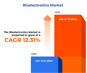
Key Applications in 2026 Healthcare
The integration of electronics into biocompatible substrates has led to a new class of medical devices that were once the domain of science fiction.
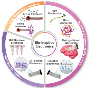 Schematic overview of emerging strategies for bio-inspired electronics and neural interfaces
| Neural Interfaces and “Living Electrodes”. From simple deep brain stimulation, we are moving towards Biohybrid Neural Interfaces that use tissue-engineered axons to bridge the gap between a computer chip and the motor cortex. By “growing” biological wires into the brain, these devices achieve a level of chronic stability that allows paralysed patients to control robotic limbs with the same fluid precision as a biological arm.
Soft Bio-Sensing Wearables: Modern-day wearables have moved from the wrist to the skin. “Electronic skin” (e-skin) patches—ultrathin, breathable, and biocompatible—now monitor biochemical markers in sweat, such as cortisol and glucose, in real-time. These devices utilise MXenes and Graphene to detect molecular changes at concentrations previously only reachable via blood draws. |
| Closed-Loop Bioelectronic Medicine: The concept of “electroceuticals” is now a clinical reality. Small, biocompatible devices implanted on the vagus nerve can monitor inflammatory markers and automatically deliver precise electrical pulses to inhibit the “cytokine storm” associated with autoimmune diseases like rheumatoid arthritis and Crohn’s disease. |
Some key challenges remain to be resolved:
Engineering Challenges:
- Stability and Bio-Integration
Despite the progress, engineering the interface remains a complex task. The physiological environment is incredibly harsh—warm, salty, and chemically active—leading to the degradation of many synthetic materials.
- Hermetic Packaging vs. Biocompatibility
Engineers must find a critical balance between the need to seal sensitive electronics from moisture while ensuring the outer layer is soft enough to integrate with tissue. In 2026, atomic layer deposition (ALD) is used to create nanometer-thin ceramic coatings that provide moisture barriers without adding stiffness.
- The Power Problem
Traditional batteries are bulky and toxic. Next-generation devices are increasingly powered by biofuel cells that harvest energy from blood glucose or through ultrasonic power transfer, which allows deep-seated implants to be recharged wirelessly through layers of muscle and bone
Ethics and the Regulatory Challenges
- As we successfully integrate electronics into the human body, the ethical implications have shifted from “safety” to “agency and privacy.”
- The EU Medical Device Regulation (MDR) and the FDA’s Digital Health Centre of Excellence have established new frameworks for “Neural Data Privacy.”Since these devices can read and potentially influence neural states, the data they produce is classified as a biological asset.
- Furthermore, the longevity of these devices raises questions about “hardware obsolescence” in living patients. Engineering the interface now includes a roadmap for software updates and long-term support for implants that may stay in the body for decades.
The Future: Toward “Living” Bioelectronics
The trend is moving toward synthetic biology-electronics hybrids. We are seeing the prototypes of devices where genetically engineered cells that produce an electrical signal work as “Sensors” when they detect a specific pathogen or cancer marker.
By engineering the interface at the molecular level, we are not just repairing the body; we are enhancing its resilience.
The integration of electronics into biocompatible materials is more than a technical achievement—it is the foundation of a new era of personalised medicine where the device and the patient are the same.
The post Engineering the Interface: Integrating Electronics into Biocompatible Materials for Next-Generation Medical Devices appeared first on ELE Times.
EU–India FTA: A Defining Moment for India’s Electronics and Semiconductor Industry
As global electronics and semiconductor supply chains are restructured for resilience and trust, the proposed EU–India Free Trade Agreement (FTA) is emerging as a pivotal opportunity for the Indian industry. More than a tariff-reduction exercise, the agreement has the potential to integrate India more deeply into Europe’s advanced electronics and semiconductor value chains. For India, the FTA represents a transition—from cost-driven manufacturing to value-driven, technology-led partnership.
The European Union is one of the world’s most quality-conscious electronics markets, with strong demand across automotive electronics, industrial automation, medical devices, power electronics, renewable energy systems, and telecom infrastructure. Under the EU–India FTA, reduced tariffs and streamlined regulatory frameworks will enhance the competitiveness of Indian electronics products.
Alignment on conformity assessment and technical standards will shorten qualification cycles and lower compliance costs, enabling Indian manufacturers to integrate directly into EU OEM and Tier-1 supply chains. As European companies pursue China-plus-one sourcing strategies, India stands to gain as a reliable and scalable manufacturing base.
India’s electronics industry has historically been assembly-led, but this is changing rapidly. Supported by policy incentives and growing design capabilities, Indian firms are expanding into PCB assembly, system integration, testing, and engineering services.
The EU–India FTA accelerates this shift by encouraging European OEMs to localise higher-value activities in India. Electronics manufacturing services (EMS) providers, component manufacturers, and design-led companies can leverage European partnerships to move beyond box build toward design-for-manufacturing, reliability engineering, and lifecycle management—key to long-term competitiveness.
Semiconductors are central to the EU–India technology partnership. The FTA aligns closely with India’s Semiconductor Mission and the EU Chips Act, creating a stable framework for collaboration across design, packaging, testing, and advanced manufacturing.
India’s strengths in chip design, embedded systems, and engineering talent complement Europe’s leadership in semiconductor equipment, materials, power electronics, and automotive-grade chips. Reduced barriers for capital equipment, technology transfer, and skilled workforce mobility can accelerate joint investments in OSAT, ATMP, and speciality semiconductor manufacturing.
This collaboration positions India as a trusted node in Europe’s semiconductor supply chain diversification efforts.
Beyond large fabs and design houses, the FTA creates opportunities for component and equipment suppliers. Demand for sensors, power modules, passive components, connectors, precision tooling, and clean-room equipment is expected to rise as European electronics and semiconductor companies expand operations in India.
Indian MSMEs operating in these segments can integrate into European Tier-2 and Tier-3 supply chains, benefiting from long-term sourcing contracts, technology upgrades, and exposure to global quality benchmarks.
The EU–India FTA also strengthens innovation linkages. Indian start-ups working in semiconductor IP, AI-enabled hardware, EV electronics, power electronics, and Industry 4.0 solutions will gain improved access to European R&D ecosystems, pilot customers, and funding platforms.
Europe’s strong IP regimes and industrial testbeds offer Indian deep-tech start-ups a credible pathway from development to global commercialisation.
Alignment with European technical, safety, and environmental standards will enhance the global credibility of Indian electronics and semiconductor products. Standards convergence reduces certification duplication, improves supplier trust, and increases acceptance across multiple export markets. For global buyers, this translates into confidence in Indian suppliers—an essential requirement in electronics and semiconductor sourcing.
The EU–India FTA arrives at a defining moment for the electronics and semiconductor industry. With effective execution, it can accelerate India’s shift from assembly-led operations to value-added manufacturing, design, and innovation. More importantly, it positions India as a strategic, trusted partner in global electronics and semiconductor supply chains—built on quality, resilience, and long-term collaboration.
Devendra Kumar
Editor
The post EU–India FTA: A Defining Moment for India’s Electronics and Semiconductor Industry appeared first on ELE Times.
Making my first circuit with a breadboard.
 | I’m really excited to try some circuits and build a decimal to binary/hexadecimal game. I’m in school for automation and robots, smart manufacturing and industrial technology, so I have a base knowledge of how circuits work. I’ve never used a breadboard, we mostly wire up components to make a complete circuit, more so electrician work. I also got a solder iron recently. I’m really excited and wanted to share. I’ll definitely be back to show the finished project. The breadboard is smaller but I’m sure it’s enough for a beginner. For the most part, I know what the included parts are for. I am excited to get into this! [link] [comments] |
A hard-life Tile Mate goes under the knife

This engineer was curious to figure out why the Bluetooth tracker for his keys had abruptly gone deceased. Then he remembered a few-year-back mishap…
My various Tile trackers—a Mate attached to my keychain (along with several others hidden in vehicles)—and a Slim in my wallet, have “saved my bacon” multiple times over my years of using them, in helping me locate misplaced important items.

But they’ve been irritants as well, specifically in relation to the activation buttons and speakers built into them. Press the button, and the device loudly plays a little ditty…by default, it also rings whatever smartphone(s) it’s currently paired with. All of which is OK, I guess, as long as pressing the button was an intentional action.
However, when the keychain and/or wallet are in my pockets, the buttons sometimes also get pressed, as well…by keys or other objects in my front pocket, credit cards in my wallet, or sometimes just my body in combination with the pants or shorts fabric. That this often happens often when I’m unable to easily silence the din (while I’m driving, for example) or at an awkward moment (while I’m in the midst of a conversation, for example), is…like I said, irritating.
Silence isn’t always blessedI eventually figured out how to disable the “Find Your Phone” feature, since I have other ways of determining a misplaced mobile device’s location. So my smartphone doesn’t incessantly ring any more, at least. But the tracker’s own ringtone can’t be disabled, as far as I can tell. And none of the other available options for it are any less annoying than the “Bionic Birdie” default (IMHO):

That said, as it turns out, the random activations have at least one unforeseen upside. I realized a while back that I hadn’t heard the tune unintentionally coming from the Tile Mate on my keychain in a while. After an initial sigh of relief, I realized that this likely meant something was wrong. Indeed, in checking the app I saw that the Tile Mate was no longer found.
My first thought (reasonable, I hope you’ll agree) was that I had a dead CR1632 battery on my hands. But to the best of my recollection, I hadn’t gotten the preparatory “low battery” notification beforehand. Indeed, when I pulled the coin cell out of the device and connected it to my multimeter’s leads, it still read a reasonable approximation of the original 3V level. And in fact, when I then dropped the battery into another Tile Mate, it worked fine.
A rough-and-tumble pastSo, something inside the tracker had presumably died instead. I’d actually tore down a same-model-year (2020) Tile Mate several years back, that one brand new, so I thought it’d be fun to take this one apart, too, to see if I could discern the failure mechanism via a visual comparison to the earlier device.
At this point, I need to confess to a bout of apparent “senioritis”. This latest Tile Mate teardown candidate has been sitting on my bookshelf, queued up for attention for a number of months now. But it wasn’t until I grabbed it a couple of days ago, in preparation for the dissection, that I remembered/realized what had probably initiated its eventual demise.
Nearly four years back, I documented this very same Tile Mate’s inadvertent travel through the bowels of my snowblower, along with its subsequent ejection and deposit in a pile of moist snow and overnight slumber outside and to the side of my driveway. The Tile Mate had seemingly survived intact, as did my keys. My Volvo fob, on the other hand, wasn’t so lucky…

Fast-forward to today, and the Tile Mate (as usual, and as with successive photos, accompanied by a 0.75″/19.1 mm diameter U.S. penny for size comparison purposes) still looks reasonably robust, at least from the front:

Turn it around, on the other hand…see that chip in the case above the battery compartment lid? I’d admittedly not noticed that now-missing piece of plastic before:

Arguably, at least theoretically, the lid’s flipside gasket should still preclude moisture intrusion:


But as I started to separate the two case halves:

I also noticed cracks at both battery compartment ends:


Again, they’re limited to the battery area, not intruding into the glue-reinforced main inner compartment where the PCB is located. But still…


And what’s with that additional sliver of grey plastic that got ejected during the separation?

As you may have already figured out, it originated at the keyring “hole”:

After it initially cracked (again, presumably as a result of the early-2022 snowblower debacle) it remained in place, since the two case halves were still attached. But the resultant fracture provided yet another environmental moisture/dirt/etc. intrusion point, albeit once again still seemingly counteracted by the internal glue barrier (perhaps explaining why it impressively kept working for four more years).
Here’s a reenactment of what the tracker would have looked like if the piece had completely fallen out back then:

See, it fits perfectly!

Here’s what this device’s PCB topside looks like, flush with test points:

Compared to its brand-new, same-model-year predecessor, I tore down nearly five years ago:

Same goes for this device’s PCB underside, notably showcasing the Nordic Semiconductor nRF52810 Bluetooth 5.2/BLE control SoC, based on an Arm Cortex-M4, and the associated PCB-embedded antenna along one corner:

versus the pristine one I’d dissected previously:

I don’t see a blatant failure point. Do you? I’m therefore guessing that moisture eventually worked its way inside and invisibly did its damage to a component (or few). As always, I welcome your theories (and/or other thoughts) in the comments!
—Brian Dipert is the Principal at Sierra Media and a former technical editor at EDN Magazine, where he still regularly contributes as a freelancer.
Related Content
- Teardown: Tile Mate Bluetooth tracker relies on software
- Examining an environmental antonym: Tile’s Slim
- This wearable Bluetooth device can be your personal radiation tracker
- Revolutionizing Tracking with LoRaWAN Technology
The post A hard-life Tile Mate goes under the knife appeared first on EDN.
Qorvo’s quarterly revenue grows a more-than-expected 8.4% year-on-year
Open source PCB designed around STM32F405RGT6 for rocket / drone applications.
 | Custom PCB designed around STM32F405RGT6 for rocket / drone applications. MCU
Interfaces & IO
Notes
[link] [comments] |
Future-Proofing Bharat: India’s Multi-Billion Dollar AI Strategy Revealed
India is hosting the AI Impact Summit 2026 under the Ministry of Electronics and Information Technology, this month from February 16-20. The Summit has received a phenomenal response from across the world, and is shaping up to be the biggest such event so far globally, said Union Minister Ashwini Vaishnaw on Friday.
The summit week will feature around 500 curated events across Bharat Mandapam and Sushma Swaraj Bhawan. The AI Impact Expo will host over 840 exhibitors, including country pavilions, Ministries, State governments, industry, start-ups, and research institutions, showcasing AI solutions with proven real-world impact.
The conference has confirmed the participation of 15 Heads of State Government, more than 40 Ministers, over 100 leading CEOs and CXOs, and more than 100 eminent academics. Industry partners, including Jio, Qualcomm, OpenAI, Nvidia, Google, Microsoft, Adobe, and the Gates Foundation, are expected to participate in the event.
The Minister also informed that leading IT companies had developed over 200 focused and sector-specific AI models, expected to be launched during the upcoming summit. With investments worth nearly $70 billion already flowing into the AI infrastructure layer, the potential to double it by the conclusion of the event is exponential, he added. The AI talent pool is expected to be scaled up by extending infrastructure and industry-finalised curricula to 500 universities.
Budget Highlights for the AI Sector
Additionally, the government has proposed to focus on developing the AI landscape in India with specific provisions in the Union Budget 2026-27. As the focus shifts to building the digital infrastructure, the government has proposed an additional investment of USD 90 billion, specifically for the AI Data Centres and further encouraged long-term investments by proposing a tax holiday till 2047 for foreign companies providing cloud services to customers globally using data centre services from India. Such companies will provide services to Indian customers through an Indian reseller entity. Simultaneously, a safe harbour of 15 per cent on cost has also been proposed where the data centre service provider in India is a related entity.
The government has proposed several domains for AI integration in the Indian landscape: –
- Governance: Serving as a force multiplier for improved public service delivery.
- Supporting new technologies: Adopting new technologies in various sectors through the AI Mission and National Quantum Mission.
- Labour market analysis: Assessing the impact of emerging tech such as AI on job roles and skill requirements.
- Bharat-VISTAAR: A new multilingual AI tool designed for broader linguistic accessibility.
- Agriculture: Integration with AgriStack portals and ICAR agricultural practice packages.
- Healthcare & accessibility: R&D and integration into assistive devices for People with Disabilities manufactured by Artificial Limbs Manufacturing Corporation of India (ALIMCO).
- Customs & security: Expanding non-intrusive scanning and advanced imaging for risk assessment.
- Education: Embedding AI modules directly into the national education curriculum from school level onwards and for teacher training.
- Professional development: Upskilling and reskilling programs for engineers and tech professionals.
- Employment matching: AI-enabled platforms to connect workers with jobs and training opportunities.
India’s AI Landscape
Since 2020, the Artificial Intelligence (AI) start-up ecosystem in India has experienced rapid growth, with over 150 native AI start-ups having raised over $1.5 billion in funding as of September 2025.
As of early 2026, there are over 1,900 total AI companies in India, with 555 being funded. AI start-ups have touched several industries to provide a technically advanced perspective to the workings in the industry, from healthcare, agriculture, Aerospace & Defence, navigation, to education, manufacturing, banking, and E-commerce. Some notable start-ups include Sarvam AI, Krutrim, Observe.AI, Avaamo, Nanonets, and Atomicwork in the sector.
Global giants like IBM, Google, Microsoft, OpenAI, and Nvidia have established or expanded their R&D centres, engineering hubs, and regional offices in India to leverage the country’s vast tech talent pool and rapidly expanding digital economy. Domestic players like Perplexity has partners with telecom giants like Airtel to expand their reach. Simultaneously, Anthropic, the AI start-up backed by Google and Amazon, plans to open its first Indian office in Bengaluru in early 2026, focusing on AI tools and tapping into the local developer ecosystem.
Future of AI in India
The AI market is projected to reach $126 billion by 2030, with a long-term contribution of $1.7 trillion to India’s GDP by 2035.
These developments, coupled with the government’s initiative to boost the sector and focus on “Sovereign AI” to reduce dependency on foreign technology and build custom chips within 3-5 years, can position India as a formidable force in the sector of Artificial Intelligence globally, while the country already ranks third globally in AI competitiveness.
By: Shreya Bansal, Sub-Editor
The post Future-Proofing Bharat: India’s Multi-Billion Dollar AI Strategy Revealed appeared first on ELE Times.
Budget 2026-27: India Semiconductor Mission 2.0 Announced to Boost 3 nm & 2 nm technology nodes in India
The Union Budget 2026-27 outlines the continuation of India’s deep commitment to the domestic semiconductor ecosystem, aiming to promote it to new heights. Union Finance Minister Smt Nirmala Sitharaman, in the Union Budget 2026-27, announces the launch of India Semiconductor Mission 2.0 (ISM 2.0). It will be a continuation of the earlier ISM 1.0 with a realigned goal to produce equipment and materials, design full-stack India IP, and solidify supply chains, a milestone for the technology sector. ‘This time the mission carries a broad mandate to enable the next level of India’s electronic stride into products and more IPs, precisely.
“ISM 1.0 expanded India’s semiconductor sector capabilities. Building on this, we will launch ISM 2.0 to produce equipment and materials, design full‑stack Indian IP, and fortify supply chains. We will also focus on industry‑led research and training centres to develop technology and a skilled workforce,” she said.
Upgrading India’s Semiconductor Ecosystem
Shri Ashwini Vaishnaw, Union Minister of Railways, Electronics and Information Technology, said that the Budget has announced the launch of India Semiconductor Mission (ISM) 2.0, building upon the strong foundation created under ISM 1.0, which established a completely new and foundational semiconductor industry in India.
ISM 2.0 will focus on designing and manufacturing semiconductor equipment in India, manufacturing of materials used in semiconductor production, creation of a large design ecosystem, and further strengthening of talent development initiatives. A provision of Rs. 1,000 crore has been made for ISM 2.0 for FY 2026-27.
Support for Fabless Startups
The mission launch finds mention in the Budget 2026-27 with a fresh outlay of ₹1,000 crore allocation in the BE fiscal 2027. Vaishnaw said recently that the government plans to support at least 50 fabless chip companies in ISM 2.0 by scaling up the Design Linked Incentive Scheme, with the long-term goal of producing “one AMD” and “one Qualcomm” from India.
“The Union Budget 2026–27 charts a decisive course for India’s evolution into a global technology leader. The enhanced capital outlay of ₹12.2 lakh crore and the launch of the India Semiconductor Mission 2.0 reaffirm the government’s commitment to deep-tech indigenization,” says Mr. Meenu Singhal, Regional Managing Director, Socomec Innovative Power Solutions.
Talking about the budget Mr Pankaj Mohindroo, Chairman, ICEA, says, “Budget 2026–27 reinforces the government’s commitment to manufacturing-led growth, particularly in electronics and semiconductors, through continuity, scale, and targeted reforms. Measures such as the expansion of ECMS, support for ISM 2.0, and long-term incentives for cloud and data infrastructure send a strong signal of strategic intent and policy stability.
The post Budget 2026-27: India Semiconductor Mission 2.0 Announced to Boost 3 nm & 2 nm technology nodes in India appeared first on ELE Times.
Caliber Interconnects Achieves ARAI Certification for EV Charging Solutions, Strengthening India’s Indigenous EV Infrastructure
Caliber Interconnects Private Ltd., a leading Indian engineering and deep-tech solutions company, today announced that its electric vehicle (EV) charging portfolio has been awarded ARAI certification, marking a significant milestone in the company’s journey to deliver reliable, safe, and future-ready charging infrastructure for India’s rapidly evolving mobility ecosystem.
The certification from the Automotive Research Association of India (ARAI) validates Caliber’s adherence to stringent national standards for safety, performance, and environmental compliance—benchmarks critical to the Indian automotive and EV industries.
“This milestone goes far beyond a certificate—it’s a clear signal of our engineering depth and long-term commitment to India’s EV future,” said Suresh Babu, Founder & CEO, Caliber Interconnects. “ARAI certification reinforces our belief that India deserves globally competitive EV charging solutions that are designed, manufactured, and supported locally. At Caliber, we are building high-performance charging systems that the ecosystem can depend on—not just today, but for the decade ahead.”
A Comprehensive, ARAI-Certified EV Charging Portfolio
Caliber Interconnects offers one of the industry’s most versatile EV charging portfolios, addressing residential, commercial, fleet, and public charging needs:
- AC Chargers: 3.3 kW | 7.4 kW | 22 kW
- Hybrid Chargers: 30 kW DC + 22 kW AC
- DC Fast Chargers: 30 kW | 60 kW | 120 kW | 240 kW
- Two-Wheeler DC Chargers: 3 kW | 6 kW
All chargers are powered by Cogency, Caliber’s intelligent smart-charging platform engineered for real-time monitoring, predictive maintenance, and optimized charger performance.
Intelligent, Scalable, and Standards-Compliant
Cogency is OCPP 1.6 and 2.0.1 compliant and supports both Android and iOS, enabling seamless system integration, remote management, and scalable deployments across diverse charging networks. The platform is designed to meet the operational demands of utilities, charge point operators, OEMs, and infrastructure developers.
With ARAI certification, Caliber’s EV chargers meet the highest standards expected by India’s automotive industry—ensuring safety, durability, and environmental responsibility across operating conditions.
Designed in India. Built for Scale.
At a time when the market is saturated with imported EV chargers, Caliber Interconnects is championing locally manufactured, future-ready solutions that reduce dependency, improve serviceability, and strengthen India’s EV value chain.
Whether supporting immediate deployments or long-term infrastructure planning, Caliber’s charging solutions are engineered to scale alongside the growing demands of India’s EV and clean-energy ecosystem.
The post Caliber Interconnects Achieves ARAI Certification for EV Charging Solutions, Strengthening India’s Indigenous EV Infrastructure appeared first on ELE Times.
Сторінки


![[link]](https://i.redd.it/2griqc30k9hg1.jpeg)
![[link]](https://i.redd.it/28w6ib63a4hg1.jpeg)