
Збирач потоків
EPC adds 3-phase BLDC motor drive inverter evaluation board for humanoid robot joint applications
Infineon presents MCU and sensor solutions for the future of AI, IoT, mobility, and robotics
Next-generation embedded systems are essential for applications in the rapidly evolving connected world. They range from high-performance sensors for capturing critical data to advanced microcontrollers (MCUs) that process and analyse this data. At Embedded World 2026, taking place from March 10 to 12, 2026, in Nuremberg, Germany, Infineon Technologies AG will demonstrate how its innovative semiconductor solutions enable green and efficient energy, clean and safe mobility, and an intelligent and secure IoT. True to the motto “Driving decarbonization and digitalisation. Together,” the Infineon booth in Hall 4A, booth 138, will present highlights for applications ranging from AI and IoT to automotive and robotics that contribute to a more sustainable future.
Infineon’s highlight topics at embedded world 2026
Microcontrollers – the core of embedded intelligence: MCUs are the central processing units of modern embedded systems, coordinating control, computation, and connectivity in countless applications. In Nuremberg, Infineon will demonstrate its comprehensive MCU portfolio through live demos that illustrate real-world use cases, such as:
- Edge AI and robotics demonstrations, where Infineon PSOC and AURIX MCUs enable deterministic real-time processing, adaptive control, advanced safety, and secured connectivity
- Demos targeting software-defined vehicles, including the TRAVEO SDV Zonal Demo, highlighting how automotive MCUs support zonal E/E architectures, OTA updates, and software-driven innovation
- Industrial and IoT applications, showing how energy-efficient MCUs combine performance, safety, and cybersecurity to enable smart devices and enable manufacturers to comply with the upcoming European Cyberresilience Act (CRA)
XENSIV sensors – bridging the physical and digital worlds:
Sensors act as the interface between the real world and digital processing, enabling precise data acquisition for control, monitoring, and decision-making processes. At Embedded World 2026, Infineon will present its XENSIV sensor portfolio, demonstrating how sensor data powers advanced systems across automotive, industrial, and consumer electronics. The demos include:
- Robotics and Edge AI demos in which Infineon XENSIV sensors enable robots to see, hear, and feel, providing the environmental and contextual awareness required for safe interaction and autonomous behaviour
- Automotive and SDV-related use cases, showcasing how radar, magnetic, and current sensors support perception, monitoring, and zonal architectures in modern vehicles
- IoT and industrial demonstrations,s including the next generation XENSIV CMOS 60 GHz radar for IoT. These illustrate how MEMS microphones and other XENSIV sensors deliver reliable, high-fidelity data for connected and energy-efficient devices
In addition, Infineon experts will be giving in-depth presentations demonstrating how the company’s MCU and sensor solutions enable efficient, secure, and rapid innovations in areas such as AI, robotics, IoT, and software-defined vehicles.
The post Infineon presents MCU and sensor solutions for the future of AI, IoT, mobility, and robotics appeared first on ELE Times.
UV LED prices rising by 5% in Q1 due to increased material and labor costs
Proud to say I finally got my hands on a RIGOL DHO804
 | submitted by /u/ieatgrass0 [link] [comments] |
Compound semiconductor materials market growing at 14% CAGR to almost $5.2bn by 2031
Simple shorts sniffer

Recently, frequent and favorite contributor Nick Cornford gave us a cool and novel acoustic-interface design for a super sub-ohmmeter capable of audibly sniffing out defects in PWBs: “Tuneful track-tracing.”
Figure 1’s design shamelessly nicks Cornford’s concept. It stretches the resistance sensing range by a few decades, thus spanning single-digit milliohms to double-digit ohms. This adds extra versatility for locating spurious connections in both loaded boards and boards with shorts in ground planes. Here’s how it works.

Figure 1 Audible milli-ohmeter output frequency is linear versus resistance over several orders of magnitude.
Wow the engineering world with your unique design: Design Ideas Submission Guide
A 50-mA excitation current is provided to the PWB under test by R5 via connections A (source) and B (half-Kelvin sense and current return). D1 limits the maximum developed voltage to ~700 mV. This prevents (potentially damaging) forward bias of components on loaded boards in case the short being sniffed unexpectedly disappears.
The current return side of B consists of the (approximately) known resistance (44 mΩ) of a 41-inch length of 24 AWG copper wire. The resulting 44 m x 0.05 A = ~2 mV drop provides a null reference for the A1a voltage to current amplifier. We’ll discuss that more shortly (no pun?).
The probe voltage mode signal is converted to current mode by transconductance amplifier Q1/A1a, the associated resistor network, and range selection switch S1. R6 provides static-discharge protection for A1’s input pin while developing only uV of offset from A1’s pA-level bias current. S1 provides two frequency/resistance ranges: 100 Hz/Ω and 10 kHz/Ω.
The shorts-sniffing process consists of sliding probe C along the problematic path on the PWB while listening to the resulting audio output. Its frequency rises or falls with the resistance between the probe contact and the Kelvin connection B rises or falls. Maximum resolution results if a quick initial nulling of offset voltage is done via Null pot R1 adjustment. It provides up to ±2 mV of input offset adjustment to cancel the op-amp offset for a zero (or near) Hz output when probe C is held at the point of excitation current entry to the PWB under test. Of course, you won’t hear the actual fundamental frequency when oscillation is that slow, but only the (annoying) buzz of the square wave rising and falling edges.
The A1b (more or less symmetrical) triwave/squarewave oscillator itself is built around the 2way current mirror comprising Q2, Q3, and D2 as described in this earlier DI: “A two-way mirror—current mirror that is.”
The mirror sources current into timing cap C1, linearly ramping it up, when A1b’s pin 7 is positive, and sinks current when pin 7 is low, ramping it down. The resulting 1Vpp triwave on C1 and the squarewave on pin 7 are approximately symmetrical.
Its actual frequency can be over the range from the subsonic to the ultrasonic, but of course (by definition), little information will be relayed to your ear by either. Thence cometh the utility of range switch S1.
Stephen Woodward‘s relationship with EDN’s DI column goes back quite a long way. Over 200 submissions have been accepted since his first contribution back in 1974. They have included best Design Idea of the year in 1974 and 2001.
Related Content
- Tuneful track-tracing
- A two-way mirror—current mirror that is
- A current mirror reduces Early effect
- Active two-way current mirror
The post Simple shorts sniffer appeared first on EDN.
Згадуємо тих, завдяки кому Україна вистояла у лютому 2022 й продовжує боротьбу

Сьогодні - четверті роковини початку повномасштабного російського вторгнення. Ми згадуємо 24 лютого 2022 року і тих, завдяки кому Україна вистояла тоді й продовжує боротьбу сьогодні.
Пам'яті Володимира Мужа

🕯 На війні загинув випускник нашого університету Володимир Муж (12.05.2001 — 05.02.2026)
R&S advances AI-RAN testing using digital twins in collaboration with NVIDIA
Rohde & Schwarz will showcase a new milestone in AI-driven wireless system testing at MWC Barcelona. The testbed, developed in collaboration with NVIDIA, integrates hardware-in-the-loop site-specific channel emulation using the NVIDIA Sionna Research Kit, enabling testing of AI-RAN applications under realistic channel conditions. The demonstration highlights the long-term collaboration of Rohde & Schwarz and NVIDIA, focusing on prototyping and validation of AI-RAN innovation with cutting-edge test and measurement solutions.
Evolving from prior proofs-of-concept in advanced neural receiver design – including custom constellations for pilotless communication – the new testbed advances from link-level validation to system-level verification using the full 5G NR protocol stack.
Powered by a single NVIDIA DGX Spark, the NVIDIA Sionna Research Kit runs a software-defined 5G RAN based on OpenAirInterface, while supporting AI inference workloads that comply with the strict real-time constraints of wireless systems. To showcase the flexibility of the research platform, a novel AI/ML-enhanced link adaptation algorithm has been integrated into the end-to-end system. It dynamically adjusts the downlink modulation and coding scheme (MCS) to optimise spectral efficiency and link reliability. The AI-driven link adaptation can learn not only site-specific propagation characteristics but also user equipment-specific behaviour on the fly, emphasising the need for end-to-end testbeds that capture these effects.
The testbed integrates the R&S SMW200A vector signal generator featuring dynamic channel emulation capabilities and the FSW signal and spectrum analyser. Jointly, these instruments enable the emulation of complex site-specific radio channels, seamlessly interfacing with the NVIDIA Sionna RT differentiable ray-tracing software. This closed-loop setup enables researchers and developers to evaluate the performance of novel AI-driven RAN features under dynamic, site-specific RF conditions – all without leaving the lab.
Gerald Tietscher, Vice President Signal Generators, Power Supplies and Meters at Rohde & Schwarz, said: “We’re excited to continue our ongoing collaboration with NVIDIA with this latest proof-of-concept for testing AI-enhanced base stations for both 5G-Advanced and 6G under realistic propagation conditions. Leveraging digital twin technology and ray tracing, this approach aims to bridge the gap between AI-driven wireless simulations and real-world deployment, facilitating more efficient and accurate testing of next-generation receiver architectures.”
Soma Velayutham, global industry business development lead for telecommunications at NVIDIA, said: “Synthetic data generation is transforming the way we train and validate AI-RAN systems by ensuring accuracy, scalability, and privacy, especially in settings of sparse data. Rohde & Schwarz, leveraging the NVIDIA Sionna Research Kit, exemplifies how industry-leading expertise and innovative technology can come together to accelerate progress in this critical field.”
The post R&S advances AI-RAN testing using digital twins in collaboration with NVIDIA appeared first on ELE Times.
A real-world approach for AI-driven semiconductor manufacturing

The semiconductor manufacturing industry faces an unprecedented data challenge. For the newest devices, test programs can contain over a million test items, generating gigabytes of data per chip across probe, assembly, and test operations. The largest deployments have reached the multi-petabyte range, creating a fundamental problem: traditional business intelligence tools simply cannot handle semiconductor-scale data with millions of columns and rows.
Public comments from three semiconductor executives sum up the challenge. “As a result of the increased complexity of advanced packaging, the amount of manufacturing and test data that semiconductor companies need to analyze has increased sixfold since 2022,” recently commented Mike Campbell, Qualcomm’s chief supply chain Officer.
At the same event, Aziz Safa, corporate VP and GM of Intel Foundry Automation, had this to say: “We have 600 petabytes of data across Intel. The challenge that we have is to be able to run algorithms in the areas where we need that data to solve problems.”
And John Kibarian, CEO of PDF Solutions, mirrored those remarks. In many cases, he said, no more than 5% of the collected semiconductor manufacturing data is used in analytics. Yet more than ever, access to timely analytics is critical to quickly ramp the yield of new advanced process nodes or ensure the quality of complex packages. In this context, it’s critical to find new innovative ways to scale the ability to analyze semiconductor data.
One comprehensive strategy includes a plan to enhance the capability of a data platform, already widely used across the semiconductor industry, to address this challenge by combining scalable analytics infrastructure with advanced AI capabilities, including large language models (LLMs) and autonomous agents.
This approach represents a fundamental rethinking of how semiconductor manufacturers can extract actionable insights from massive, complex datasets.
The scalability problem
Traditional business intelligence (BI) tools face critical limitations in semiconductor manufacturing environments. They rely on local memory, which severely restricts analysis and machine learning capabilities. They also lack computational and organizational scalability often related to the specific characteristics of semiconductor data that may have hundreds of thousands or even millions of parameters to analyze.
Think of a table with a million columns and hundreds of thousands of rows. Visualizing this type of dataset in a traditional data analytics or BI tool has reached its limit, and this approach will not address the future needs of an industry where data size and complexity keep increasing.
Typically, engineers develop bespoke scripts based on summary statistics disconnected from the original data sources, and these scripts are typically served without the infrastructure for robust sharing across the organization.
One answer is a new parallel and distributed data architecture with dynamic partitioning. Rather than bringing raw data to the client for analysis, the system keeps data in the server layer and delivers only the visualizations needed by users. This thin-client approach enables the system to scale dynamically based on current needs by caching in the data layer for faster access and pre-configured analytics running continuously across all available data.
The results are striking. Benchmark testing shows approximately 25-fold performance improvements on typical large test programs with the ability to work with one million test items and beyond, a scale of analysis previously impossible.
The system achieves this through parallelizable performance across both rows (individual die) and columns (test parameters), combining static compute nodes with burst cloud computing for cost-effective scaling to extremely large datasets.
Deploying AI models at scale across enterprise
Deploying AI in semiconductor manufacturing requires more than just training models; it demands a complete operational infrastructure. The infrastructure’s architectural strategy addresses three major operational challenges: deployment bottlenecks caused by manual handoffs and brittle integrations; data friction from building custom pipelines instead of leveraging existing systems; and governance risks from poor lineage between production models and training parameters.
One tool gaining market traction used by data scientists from code to production for semiconductor data is focused on deploying models at the edge. Add-on capabilities include the ability for engineers to add their own models.
An enterprise-grade model registry will enable model lifecycle governance, tracking, and sharing, with full data traceability ensuring that any model’s training inputs are always known.
Breaking down data silos
One of the most significant challenges in semiconductor manufacturing is the fragmentation of critical data across isolated systems. Yield data sits in one place, design diagnosis information in another, and equipment telemetry in yet another. This fragmentation blocks the correlation of volume yield data with physical layout features and prevents engineers from connecting specific process excursions with final yield outcomes.
One solution is extensive data integration efforts via a platform extending beyond traditional manufacturing analytics supported by a semiconductor-specific end-to-end data model.
Central to this effort is the development of a semiconductor-specific semantic data layer that maps the complex relationships between yield, design, process, and tool data. This allows alignment and linking data across domains and sources in the data platform. It also allows LLMs to interpret disparate data types as a unified whole rather than struggling with disconnected information sources.
Workflows as the foundation
A key architectural decision in the platform is to treat workflows as the internal language of the system. Every analytic operation—whether rules, machine learning pipelines, or batch analytics—is expressed as a workflow.
This provides several critical benefits. Workflows serve as the long-term memory of the system, capturing not just results, but the complete methodology used to achieve them. They can be created from learn mode, through LLMs, manually, or programmatically, and can be embedded within larger workflows for maximum reusability. Engineers may never need to directly interact with a workflow, but the capability is there when needed.
Critically, workflows act as semiconductor-specific content and context, encoding best practices as reusable playbooks. They provide transparency into how results are achieved and serve as guardrails for AI reasoning, helping prevent the hallucinations that can occur when LLMs operate without domain constraints.
The agentic LLM platform
The goal is to enable engineers to interact with manufacturing data at a higher level of abstraction. Rather than requiring deep technical knowledge of query languages and data structures, the result is a system where engineers can ask natural language questions and receive actionable insights.
Achieving this vision requires a “Semantic, Agentic, and Secure” infrastructure. The semantic layer is built on domain expertise, creating semiconductor-native knowledge graphs that encode the fundamental data hierarchy of manufacturing. This anchors LLM reasoning in the structural reality of manufacturing data, eliminating ambiguity and providing the ground truth context needed to prevent hallucinations.
For example, the system understands that CV refers to Characterization Vehicle, that yield represents the results of die binning, and that the data hierarchy flows from lot to wafer to die to package. It knows that common analytical tasks include yield trending, bin Pareto analysis, and univariate screening. This enables engineers to ask questions like “Show me the yield trend over the last week” or “What is the root cause of low yield in lot XX?” and receive meaningful, accurate responses.
The platform integrates a model context protocol for a truly agentic system. Rather than just summarizing text or answering questions, the system can autonomously plan and execute complete workflows from raw data ingestion through complex plot generation.
To ensure reliability and transparency, any agentic tasks are executed using scalable analytics workflows. They can be viewed, saved, and modified by engineers at any time to ensure total transparency of LLMs actions.
To ensure the sensitivity of semiconductor manufacturing data, a fully air-gapped, on-premises LLM infrastructure option, designed for intellectual property sovereignty, can be added. This ensures that sensitive yield data and proprietary models never leave secure firewalls, eliminating reliance on third-party cloud providers.
The path forward
A platform like this requires thorough research and development on technology selection, validation and tuning, engaging a large group of architects, developers, quality assurance specialists, designers, and product managers.
This type of platform addresses the critical industry challenge: de-risking AI adoption by securely scaling execution and maximizing return on investment from legacy data, while simultaneously future-proofing infrastructure for the rapidly emerging age of LLMs and autonomous agents.
By combining massive-scale data processing, an operational enterprise, intelligent data integration, and agentic LLM capabilities, all grounded in deep semiconductor domain expertise, the industry can be transformed. The platform can identify how value is extracted from the exponentially growing volumes of manufacturing data.
The approach suggests a future where engineers spend less time wrestling with data infrastructure and more time solving the complex yield and quality challenges that define success in semiconductor manufacturing.
 Peter L. Kostka is a Vancouver-based technology entrepreneur with a track record of scaling complex deep-tech concepts into successful commercial outcomes. Currently, he serves as the director of product management for AI at PDF Solutions, where he spearheads the AI technology roadmap and leads rapid prototyping for semiconductor and battery manufacturing sectors.
Editor’s Note
Presentations by Qualcomm’s Mike Campbell (“AI-Driven Innovation in the Semiconductor Industry”) and Intel’s Aziz Safa (“Enabling AI/ML strategy using the PDF Suite”) were given at the 2025 PDF Solutions Users Conference.
John Kibarian’s “Revolutionizing Semiconductor Collaboration: The Emergence of AI-Driven Industry Platforms” keynote was presented at SEMICON West 2025.
Related Content
- Coming Soon: Low-Cost Mini Fabs
- 5 ways manufacturers benefit from AI in chip design
- Tapping AI for Leaner, Greener Semiconductor Fab Operations
- Addressing the Biggest Bottleneck in the AI Semiconductor Ecosystem
- Unlocking compound semiconductor manufacturing’s potential requires yield management
The post A real-world approach for AI-driven semiconductor manufacturing appeared first on EDN.
Ayar Labs names Sankara Venkateswaran as VP of engineering
BluGlass secures A$190,000 order from TOPTICA for custom GaN visible lasers
NanoXplore & STMicroelectronics deliver European FPGA for space missions, first to qualify to new European ESCC 9030 standard for space applications
NanoXplore, the European leader in the design of SoC FPGA and radiation-hardened FPGA technologies, and STMicroelectronics, a global semiconductor leader serving customers across the spectrum of electronics applications, announce the qualification of NG-ULTRA for space applications. This radiation-hardened SoC FPGA has been designed specifically for space applications, including low- and medium-earth orbit constellations, and is set to be used in numerous satellite equipment systems, including flagship missions such as Galileo, Copernicus, and potentially IRIS.
“The ESCC 9030 qualification for the NG-ULTRA is a historic step. It proves that Europe now masters the entire production chain for cutting-edge digital components tailored to the requirements of both deep-space and new space constellations. Thanks to the support of the ESA, CNES, and the European Commission (via DG-DEFIS), NanoXplore & STMicroelectronics are securing EU strategic autonomy while making European satellites more competitive than ever.” — Édouard Lepape, CEO, NanoXplore.
“Space applications require a robust sovereign supply chain, radiation-hardened and cost-optimised chips. ST is leveraging its expertise in GEO and LEO platforms with proven FD-SOI technology, hardening expertise, manufacturing, advanced packaging and quality assurance assets in Europe to enable NanoXplore’s NG-ULTRA to the New Space market,” said Thomas Goust, Division General Manager of Space Division, RF & Optical Communication sub-group at STMicroelectronics.
First product certified to ESCC 9030 for the European New Space industry
This qualification marks a major industrial and technological milestone for the European space ecosystem: NG-ULTRA is the first product qualified to ESCC 9030, a new European standard dedicated to high-performance micro-circuits in flip-chip’ed on organic substrate or plastic package. This standard delivers the reliability required for space applications while enabling a transition away from traditional ceramic-packaged solutions – well-suited for deep-space but heavier and more expensive – marking a key step forward for constellations and higher-volume missions.
The “new space” dynamic (constellations, Low and Medium Earth Orbits, higher volumes) is transforming requirements for onboard digital equipment and driving a shift in scale: there is a simultaneous need for greater computing power, controlled power consumption, and contained costs compatible with large-scale deployments. NG-ULTRA addresses this challenge by enabling more data to be processed directly in orbit (edge computing), thereby limiting transmission bottlenecks between space and ground.
NG-ULTRA targets strategic functions such as on-board computers, data management and routing between sub-systems, image and video processing (real-time compression and encoding), Software Defined Radio (SDR) – enabling remote evolution of communication modes, and onboard autonomy (detection, recognition, supervision).
A secure, European supply chain
Beyond performance, this program embodies a strategic ambition to secure a sovereign and sustainable European supply chain for long-duration missions by reducing critical dependencies. For NG-ULTRA, the industrial framework combines design, manufacturing, assembly, and testing capabilities across European sites, with the aim of reconciling competitiveness, volume production, and space-grade reliability.
In addition to its own R&D and design center in Paris, Grenoble and Montpellier, NanoXplore leverages various STMicroelectronics facilities in Europe, including the Grenoble R&D and design center, the 300mm digital fab of Crolles, the space-specialist packaging facility in Rennes (France), the test and reliability site in Grenoble (France) and Agrate (Italy) and additional redundant qualified sites in Europe.
Technical specifications
With an “all-in-one” SoC (System on Chip) architecture designed specifically for platform and onboard computing applications, NG-ULTRA combines a multi-core processor with programmable hardware on a single chip. This architecture allows for greater design agility, reduces electronic board complexity and component count, and optimises latency, mass, and power consumption.
NG-ULTRA is built on STMicroelectronics’ 28nm FD-SOI digital technology platform, recognised for its advantages in energy efficiency, resistance to space radiation and advanced architecture features. Combined with a unique advanced radiation hardening technology, the NG-ULTRA is built to survive the thermal cycles, shocks, and vibrations of launch and long-term orbital life so as to ensure best-in-class performance and durability in the harsh space environment throughout the mission lifetime.
The NG-ULTRA has been designed to operate reliably in harsh radiation environments, offering a Total Ionising Dose (TID) tolerance of up to 50 krad (Si) to ensure long-term performance. It also demonstrates strong resilience to single-event effects, with Single Event Latch-up (SEL) immunity tested up to 65 MeV·cm²/mg and Single Event Upset (SEU) immunity validated for Linear Energy Transfer (LET) levels exceeding 60 MeV·cm²/mg.
NG-ULTRA integrates a full SoC based on quad-core Arm Cortex R52 and provides high computational capability (537k LUTs + 32 Mb RAM) to address the most complex onboard computer requirements.
Its streamlined architecture drastically reduces PCB complexity and system mass—two of the most critical constraints in space design. By minimising the component count, the NG-ULTRA simultaneously lowers total power consumption and project costs while increasing overall system reliability.
In addition, the SRAM-based architecture of the NG-ULTRA enables an adaptive hardware approach, allowing for unlimited on-orbit reconfiguration. This “hardware-as-software” flexibility allows operators to update functionality post-launch, adapt to evolving communication standards, or optimise the chip for different mission phases. The NG-ULTRA thus provides a future-proof platform that extends the operational relevance of assets long after they leave the launchpad.
To facilitate adoption, NG-ULTRA is also available as an evaluation kit — a complete prototyping platform that allows to rapidly validate performance and interfaces, reduces integration risks, and accelerates software and onboard logic development prior to flight-board production.
The post NanoXplore & STMicroelectronics deliver European FPGA for space missions, first to qualify to new European ESCC 9030 standard for space applications appeared first on ELE Times.
I made my own analog computer!
 | There was a lot I learned, but this was my first serious project in which I went double over budget, went over my deadline and had a lot of fun! It has 8 potentiometers, 4 inverters, 3 integrators, 2 adders, a multiplier and some. In the first image, it is running damped oscillation, which is simulating something like a mass to a spring. Here is the build on my website if anyone is interested https://paranoidrobot.neocities.org/Analogcomputerbuild [link] [comments] |
Probing a USB analog audio adapter

How do engineers squeeze all the necessary circuitry (and what is it?) into one of these devices, and do so this inexpensively?
With the demise of analog audio line out, headphone (output-only), and headset (adding mic-in) jacks in modern electronics devices—computers, smartphones, tablets, and the like—alternative methods of connecting analog audio sources and destinations are becoming increasingly common. Bluetooth-based wireless mating is certainly one option:

but the audio peripheral must also be battery-powered (and therefore potentially charge-drained when you try to use it) in this case. And quality can also be hit-and-miss depending on the lossy codec options supported (and selected) at both ends of the connection, not to mention degradation resulting from other spectrum-overlapping broadcasters.
Diminutive wired adaptersThe other common option involves instead leveraging the digital audio (plus power, along with other functions) connections that are still present in these devices. Admittedly, the Earstudio ES100 MK2 shown above can alternatively operate this way, too:

but that’s not the prevalent use case for this particular peripheral, which, anyway, is also no longer seemingly available for sale (I’ve got its successor queued up to discuss in the future). Plus, it was bulky and priced at $99; the Apple Lightning-to-3.5mm Headphone Adapter, shown below as usual (as well as with photos that follow) accompanied by a 0.75″ (19.1 mm) diameter U.S. penny for size comparison purposes:

was only $9 when Apple was selling it (when I caught wind of the pending closeout, I bought up not only the one shown above but also a few others before inventory was depleted), not to mention being self-powered over Lightning and delivering remarkably solid audio performance (and squeezing in not only the ADC and DAC but also the necessary MFi certification circuitry).
Now that Apple has transitioned its devices to USB-C, both it and Google, along with others, offer(ed, in Google’s case) diminutive, cost-effective, and performant USB-C-based successors:

I found a two-pack of them on sale for $2.09 the other day, believe it or not:

And my wife even bought me a balanced headphones-supportive USB-C adapter for Christmas!

That said, with iFixit’s “rough” teardown results as a guide (after seeing how challenging a community member’s experience was, iFixit staff stuck with x-ray analysis for their own coverage), I was loath to tackle the dissection of one of these diminutive devices myself. Instead, today I’ll be showcasing something a “bit” bigger, albeit presumably based on the same fundamental building blocks; Sabrent’s USB to 3.5mm Jack Audio Adapter, which claims to support up-to 24-bit and 96 kHz high-res audio and cost me only $6.98 on Amazon last summer:

As the above stock photo shows, and unlike one of the earlier adapters that merges both headphone and microphone functions on a common connector, this one (akin to a computer sound card, which is its target use case) splits them into two jacks; a stereo one for audio out (96 dB SNR claimed) and a separate one for the mono audio input (90 dB). Plus, the manufacturer conveniently provided a preparatory conceptual cross-section diagram, too:

From past similar experience, however, I’ve learned that such graphics don’t necessarily match reality, so I’m still going to dig inside going to satisfy my curiosity. Some box shots to start:


Inside is the adapter, safely ensconced by rubberized foam padding:

along with a few snippets of literature:


The one on the left is just the usual legal gobbledygook, in multiple languages:

Here’s our patient, first the body:


Now both ends:

See, two connectors!

The body is a mix of plastic and aluminum…I didn’t realize at first:

that the latter went all the way around the outside:

No, Brian, there’s no screw holding the chassis pieces together; it’s a single-piece assembly from the start:

Duh:

That’s much easier:

With the front panel now popped off:

the PCB now pushes right out the front, following right behind it. Connectors on top:

And…whaddya know…for a pleasant change, the C-Media CM3271 USB audio controller shown in the earlier conceptual diagram actually matches what’s on the PCB underside!

It’s no longer listed on the supplier’s website, but I still found a datasheet (PDF).
I still don’t know how other USB audio adapter manufacturers squeeze all the necessary electronics into their even more diminutive devices, but I’m also still not confident that I would have gotten the answer to that question if I’d tried (versus simply obliterating the product in the process). I’m happy with this alternative approach and end result, and I hope you are too. Agree or disagree, let me know what you think in the comments!
—Brian Dipert is the Principal at Sierra Media and a former technical editor at EDN Magazine, where he still regularly contributes as a freelancer.
Related Content
- Portable Bluetooth receiver enhances headphone-jack-deficient smartphones
- An update on music codecs
- Balanced headphones: Can you hear the difference?
The post Probing a USB analog audio adapter appeared first on EDN.
Microchip’s New MCU: A 32-bit Upgrade That Still Fits Old 8-bit Systems
Not only it's a drop-in replacement for AVR (sans SW compatibility, since it is ARM), this is first popular 32-bitter MCU that can do 5.5V I/O.\ Being multi-voltage I/O is just a cherry on top.
[link] [comments]
My first power amplifier project - Rod Elliott' P3A + P33
 | Just finished my first PA and did a sound check. Used Rod Elliott' P3A schematic but didn't order the PCB's, made my own looking at the component placement he chose. Also did the P33 DC protection and muting circuit from the schematics on his website, also my own PCB design. Ordered a BT module from Aliexpress that worked out great. Did the PCB design in KiCAD and etched the boards. Got screwed on the final transistors, found out they weighed 3 grams less than the originals so ended up ordering other ones from a supplier in Europe. Also the 10.000uF caps were counterfeit and ordered other ones. The toroidal transformer is from Aliexpress from one of those custom order vendors. Had to do an additional source for the BT module to avoid hum/ground loops. Here's how it sounds: https://youtu.be/3uhvbGdac8s?si=9sRjmpB0z5sSqoV8 Had a lot of fun building it. Can't wait for the next project! 😄 [link] [comments] |
Top Seven Tech Trends in the semiconductor sector for 2026
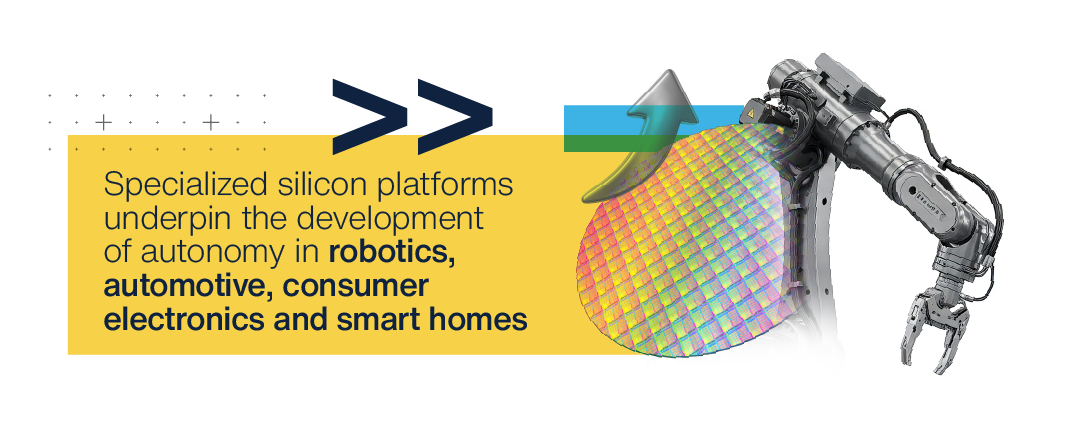
In 2026, a new class of intelligent machines will emerge. Several of the trends we’ve identified are natural extensions of those we highlighted at the start of 2025, with the new year’s advancements driven by the widespread deployment of existing technologies. Industrial sectors, robotics, automotive, consumer electronics and smart homes will all benefit from increased autonomy, underpinned by the specialised silicon platforms and advanced processing that will make this a reality.
 The foundation will continue to be semiconductor material innovation. Silicon carbide (SiC), gallium nitride (GaN) and silicon photonics will support increasing demands for efficient power conversion, thermal management, and data transmission. Architectural advances in neural processors, imaging sensors, microcontrollers and microprocessors will enhance the capabilities of autonomous and intelligent systems. Security of these systems will remain in sharp focus. In summary, our view for 2026 is: smarter machines will be built on faster and more secure semiconductor technologies.
Edge AI innovation continues to be the lynchpin connecting these trends. In 2025, we saw the momentum of more AI finding its way to the edge. For 2026, this momentum accelerates, as embedded AI finds its way into almost every category of device and sensor. These edge AI and TinyML-enabled devices will benefit from enhanced awareness and analytical capabilities, in turn enabling them to act more autonomously. We will also see the emergence of more domain- and application-specific AI chips, optimised for workloads in different environments and sectors.
The next evolution of robotics (see below), industrial systems, automobiles, smart home technology, consumer devices, and more will be supported by powerful and energy-efficient AI at the edge. In turn, these will become more active participants and partners in every aspect of our lives.
2. Robots start speaking a different languageLarge language models (LLMs) – AI trained on massive text datasets – have been dominant in the AI discussion of recent years. As highlighted last year, these advancements, along with those in neural processing, allowed machines to “think” better. A new type of model will help turn thinking into action in 2026. New large action models (LAMs), sometimes called vision-language-action (VLA) models, are enabling robots to interpret their surroundings, make decisions, and perform tasks in the physical world, which some are calling “embodied AI”.
 LAMs supporting robotic inference will drive the widespread emergence of edge AI-powered cobots working alongside humans, deployments of humanoid robots, and autonomous industrial systems that act independently with advanced sensing and motor control. The combination of enhanced intelligence and dexterity will pave the way for robotics to move from factories into retail, hospitality, and the home.
Last year, we predicted how the ability to use traditional semiconductor technologies would help advance the development of quantum computing. This has been the case, and the coming year will see quantum computers based on FD-SOI processes move from the lab to deployment. However, in 2026, the quantum-related priority for all organisations will relate to one topic: cybersecurity.
Cybercriminals are already preparing to add quantum computing to their armoury through cryptographically-relevant quantum computers (CRQCs). They are harvesting encrypted data today, confident that quantum computing will provide the power to access it in the future, which poses a real and immediate risk to every organisation. Post-quantum cryptography (PQC) provides a solution; PQC algorithm standards are being established and made available to preemptively secure devices and software. The time to act is now.
4. A tipping point for autonomous vehicles?Self-driving taxis provide the highest profile examples of the progress of autonomous vehicles, underpinned by advances in LiDAR, AI-enabled cameras, and integration with infrastructure. The number of cities around the world allowing the use or trial of so-called “robotaxis”, notably in the US and Asia, grew significantly in 2025, suggesting positive momentum. Challenges remain, with Level 4 autonomy remaining restricted to controlled environments (Level 5 being complete autonomy in any environment) and major manufacturers scaling back timelines to full autonomy.
Consumer confidence is also a barrier to adoption, though studies have shown that acceptance is far higher following use. With the opportunities increasing for consumers to experience the benefits, along with technological enhancements and efficiencies, 2026 should see progress accelerate.
5. Homes become even smarter, better connected and more secureIn 2026, several trends will converge to transform domestic technology. Edge AI, advances in connectivity protocols such as Matter and Thread, and approaches to security adopted from the commercial environment will make our homes smarter, better connected, and more secure.

Improving the collection and sharing of data between domestic devices, along with increased intelligence at the edge, will act as a force multiplier, delivering what analyst Gartner has defined as “ambient intelligence”. Among other benefits, this will allow for the creation of domestic digital twins, a concept we touched on in 2025 as an opportunity in every sector, optimising the efficiency of our homes.
As smart homes become more intelligent and connected, cybersecurity will be an increasing concern. We expect to see principles crossing over from commercial environments to the home, and in particular, best practices such as a Zero Trust approach to security in smart home technologies.
6. The integration of satellite and terrestrial networksAs we predicted in 2025, there has been no slowdown in the desire to launch more satellites into space, and particularly those low Earth orbit (LEO) satellites forming part of the communications mega-constellations. 2026 will see advancements in how these satellites are used to provide truly global connectivity. For communications network operators, the decision between traditional terrestrial networks and the growing mega-constellations of low Earth orbit (LEO) satellite networks is no longer “either/or”, but “both”. Mobile network operators are already integrating LEO networks as backhaul, filling coverage gaps in earth-based networks or to improve connection speeds.
This integrated use of networks will continue in 2026, creating a unified “network of networks” managed by AI and advancing towards goals for seamless global connectivity. The economic and educational benefits to previously unconnected parts of the globe will be huge, with significant additional enhancements to connectivity across worldwide consumer, commercial and industrial sectors.
7. A revolution in imagingImaging technology provides the foundation for many of the innovations that allow devices to operate more effectively and efficiently. Yet the central concept of lenses as stacks of curved glass to refract light has remained unchanged for centuries. Metasurface technology shifts this paradigm by recreating optical functions on perfectly flat, ultra-thin layers patterned with nanostructures. Imaging becomes smaller, less costly, and more flexible wherever it is embedded. Imaging improvements will impact every area of life, work, and industry, from more spatially-aware robotics and automobiles, to more secure devices, from enhanced photography to applications that vastly improve power efficiency.
2026 wrappedTechnology rarely moves in straight lines, but the direction is becoming clearer. The trends emerging for 2026 indicate a world shaped by greater autonomy, deeper intelligence, stronger intelligence and more, all shaped by advances in semiconductor technologies. The opportunity for organisations that understand these trajectories early enough is not simply to react but to shape what comes next. The systems designed today will define how people live, work and connect in the years to come.
The future is already taking form; it’s a matter of how boldly we choose to build it.
The post Top Seven Tech Trends in the semiconductor sector for 2026 appeared first on ELE Times.
Світла пам’ять та вічна шана Денису Гордєєву!

🕯Спільнота Київської політехніки знову в жалобі. 15 лютого 2026 року на Донеччині під час виконання бойового завдання загинув випускник КПІ Денис «Фокс» Гордєєв — лейтенант, командир взводу безпілотних авіаційних комплексів 156-ї ОМБр. Йому було 36.
Сторінки

