
Збирач потоків
TP-Link’s Kasa HS103: A smart plug with solid network connectivity

With Amazon’s smart plug teardown “in the books”, our engineer turns his attention to some TP-Link counterparts, this first one the best behaved of the bunch per hands-on testing results.
Two months back, I introduced you to several members of TP-Link’s Kasa and Tapo smart home product lines as successors to Belkin’s then-soon and now (at least as you read these words, a few weeks after I wrote them) defunct Wemo smart plug devices. I mentioned at the time that I’d had particularly good luck, from both initial setup and ongoing connectivity standpoints, with the Kasa HS103:

An example of which, I mentioned at the time, I’d shortly be tearing down both for standalone inspection purposes and subsequent comparison to the smaller but seemingly also functionally flakier Tapo EP10:

Today, I’ll be actualizing my HS103 teardown aspiration, with the EP10 analysis to follow in short order, hopefully sometime next month. What’s inside this inexpensive device, and is it any easier to disassemble than was Amazon’s Smart Plug, which I dissected last month?

Let’s find out. As usual, I’ll begin with some outer box shots of the four-pack containing today’s patient. You may call the packaging “boring”. I call it refreshingly simple. As well as recyclable.


Sorry, I couldn’t resist including that last one  .
.
Now for the device inside the box, beginning with a conceptual block diagram. Interestingly, although I’d mentioned back in December that TP-Link now specs the HS103 to handle a current draw of up to 15A, the four-pack (HS103P4) graphic on Amazon’s website still list 12A max:

Its three-pack (HS103P3) graphic counterpart eliminates the current spec entirely, replacing it with the shadowy outline of an AC outlet set, which I suppose is one way to fix the issue!

And now for some real-life shots, as usual (and as with subsequent images) accompanied by a 0.75″ (19.1 mm) diameter U.S. penny for size comparison purposes:


See that seam? I ‘spect that’ll be a key piece for solving the puzzle of the pathway to the insides:

And, last but not least, all those specs that the engineers out there reading this know and love, including the FCC certification ID (2AXJ4KP115):

Now to get inside. Although I earlier highlighted the topside seam, I decided to focus my spudger attention on the right side to start, specifically the already visible gap between the main chassis and the rubberized gasket ring:


Quickly results-realizing that I was indirectly just pushing the side plate (containing the multi-function switch) out of its normal place, I redirected my attention to it more directly:


Success, at least as a first step!


Now for that gasket…


At this point, however, we only have a visual tease at the insides:

Time for another Amazon-supplied conceptual diagram:

And now for the real thing. This junction overlap gave me a clue of how to start:


It wouldn’t be a proper teardown without at least a bit of collateral damage, yes?

Onward, I endure it all for you, dear readers:


Voilà:

Boring half first:


Now for the half we all really care about:


As with its Amazon smart plug predecessor, the analog and power portions are “vanilla”:

The off-white relay at far right on the main PCB, for example, is the HF32FV-16 from Hongfa. Perhaps the most interesting aspect of the analog-and-power subsystem, at least to me, is the sizeable fuse below the pass-through ground connection, which I hadn’t noticed in the Amazon-equivalent design (although perhaps I just overlooked it?). The digital mini-PCB abutting the relay, on the other hand, is where all the connectivity and control magic take place…

In the upper left corner is the multicolor LED whose glow (amber or/or blue, and either steady or blinking, depending on the operating mode of the moment) shines through the aforementioned translucent gasket when the switch is powered up (and not switched off):

Those two unpopulated eight-lead IC sites below it are…a titillating tease of what might be in a more advanced product variant? In the bottom left corner is the embedded 2.4 GHz Wi-Fi 1T1R antenna. And to its right is the “brains” of the operation at the other end of the antenna connection, Realtek’s RTL8710, which supports a complete TCIP/IP “stack” and integrates a 166 MHz Arm Cortex M3 processor core, 512 Kbytes of RAM and 1 Mbyte of flash memory.
Stubborn solderSpeaking of power pass-throughs…what about the other side of the main PCB? The obvious first step is to remove the screw whose head you might have already noticed in the earlier shot:


But that wasn’t enough to get the PCB to budge out of the chassis, at least meaningfully:

Recall that in the Amazon smart plug design, not only the back panel’s ground pin but also its neutral blade pass through intact to the front panel slots, albeit with the latter also split off at the source to power the PCB via a separate wire. The line blade is the only one that only goes directly to the PCB, where it’s presumably switched prior to routing to the front panel load slot.
In this design, that same switching scheme may very well be the case. But this time the back panel neutral connection also routes solely to the PCB. Note the two beefy solder points on the main PCB, one directly above the screw location and the other to the right of its solder sibling. I was unable to get either (far from both of) them either successfully unsoldered from above or snipped from below. And all I could discern on the underside of the PCB from peering through the gap were a few scattered additional passive components, anyway.
So, sorry, folks, I threw in the towel and gave up. I’m assuming that those two particular solder points, befitting the necessary stability not only electrically but also mechanically, i.e., physically, leveraged higher-temperature solid or silver solder that my iron just wasn’t up for. Or maybe I just wasn’t sufficiently patient to wait long enough for the solder to melt (hey, it’s happened before). Regardless, and as usual, I welcome your thoughts on what I was able to show you, or anything else related to this product and my teardown of it, for that matter, in the comments!
—Brian Dipert is the Principal at Sierra Media and a former technical editor at EDN Magazine, where he still regularly contributes as a freelancer.
Related Content
- Amazon’s Smart Plug: Getting inside requires more than just a tug
- How smart plugs can make your life easier and safer
- Smart plug provides remote control functionality for home devices via voice command
- Teardown: Smart plug adds energy consumption monitoring
- This smart plug automatically resets your router when your Internet goes out
The post TP-Link’s Kasa HS103: A smart plug with solid network connectivity appeared first on EDN.
EEVblog 1734 - Uni-T UT892 2000V High Voltage Multimeter TESTED
Lumentum’s quarterly revenue grows 65% year-on-year to $665.5m
✨ Запрошуємо студентів та викладачів взяти участь у HeatTech Hackathon

Теплоенергетичний кластер України разом з Київським Політехнічним інститутом імені Ігоря Сікорського запрошує студентів та викладачів на HeatTech Hackathon.
Infineon’s silicon carbide power MOSFETs selected for Toyota’s new bZ4X model
Look at these monsters! 29,000 microfarad
 | Came across this capacitor bank inside of this giant battery charger just figured I'd share, LOL. It has (3) 29k microfarad 200vdc, and (1) 13k microfarad 200vdc capacitors. Gives me the heebie-jeebies just looking at it... It has a built-in capacitor discharge button but still... [link] [comments] |
Progress on our Open Access Health Tracker
 | Wanted to share a picture of our progress on our open access health tracker. We hand assembled our first prototype (left) in 2025. Around 140 components with the smallest being 01005. Our learning: DON'T use 01005/0204 if you hand assemble. It was not a lot of fun, but we got our first prototype to work. We redesigned and improved. This time using a 4 layer flexible PCB + stiffener. AND we learned, ordering the prototypes mostly pre-assembled. However, we ran into the problem that we forgot to thermally shield our temperature related sensors (any suggestions on this very much welcome). We also ran into the issue that our 2.4GHz antenna didn't work anymore, most likely due to the PCB change, but a small cable will do the job. Now we are working on our third prototype. Integrating more sensors, compacting and fixing mistakes we made. [link] [comments] |
Відділу рідкісних та цінних документів НТБ ім. Г.І. Денисенка – 10 років!

Науково-технічна бібліотека ім. Г.І. Денисенка включає багато важливих підрозділів, які забезпечують постійну та якісну підтримку навчального і наукового процесу університету. Одні відділи існують від початку діяльності навчального закладу, інші з'явились зовсім нещодавно. Серед останніх – відділ рідкісних та цінних документів. Наприкінці осені 2025 року йому виповнилось 10 років.
The Next Phase of Energy Storage: When Batteries Start Working with the Grid
Authoredby: Rajesh Kaushal, Energy Infrastructure & Industrial Solutions (EIS) Business Group Head, India & SAARC, Delta Electronics India
For decades, the electricity grid operated on a simple principle: power had to be generated at the exact moment it was consumed. Coal plants, gas turbines, and hydro stations were dispatched to follow demand, and the grid was built around predictability and centralised control.
That principle is now being fundamentally rewritten.
As renewable energy becomes central to India’s power system, variability has entered the equation at an unprecedented scale. Solar and wind generation do not follow traditional load curves, and their growing share is changing how grids must be designed and operated. In this new reality, energy storage, particularly Battery Energy Storage Systems (BESS), is moving from being a supporting technology to becoming a core grid asset.
We are entering the next phase of energy storage, where batteries no longer sit on the sidelines but actively work with the grid.
From Backup to Backbone
In its early years, energy storage in India was largely viewed as backup power, used during outages or in niche, isolated applications. That perception is changing rapidly.
Today, batteries are expected to play a much broader role:
- Smoothing renewable variability
- Managing peak demand
- Deferring transmission upgrades
- Providing frequency and voltage support
- Enabling faster and more resilient grids
According to projections from the Central Electricity Authority, India will require over 82 GWh of total energy storage by 2026–27, with BESS contributing nearly 35 GWh, rising to 411 GWh total by 2031–32, with batteries accounting for over 236 GWh.
These are not incremental additions. They signal a structural shift in how the power system will be planned, operated, and stabilised.
When Policy Meets Scale
A key indicator of this transition is policy clarity and rapidly declining costs.
Recent tariff-based competitive bidding shows that the cost of BESS has plummeted from around ₹10.18 per kWh to approximately ₹2.1 per kWh, assuming two daily cycles. Based on market trends and utilisation patterns, the cost at 1.5 cycles per day is expected to be around ₹2.8 per kWh. This aligns closely with average solar tariffs, making storage increasingly competitive.
India’s policy framework supports this transition:
- Viability Gap Funding schemes supporting 13,220 MWh of BESS capacity with ₹3,760 crore, and an additional 30 GWh with ₹5,400 crore support through the Power System Development Fund.
- Inter-State Transmission System (ISTS) charges waiver for co-located BESS projects for 12 years and graded waivers for non-co-located projects.
- The PLI “National Programme on Advanced Chemistry Cell (ACC) Battery Storage” aims to establish 50 GWh of domestic Advanced Chemistry Cell manufacturing capacity, including 10 GWh for grid-scale applications to reduce import dependency and future costs.
These mechanisms are accelerating adoption and enhancing affordability, shifting storage from pilot projects to mainstream system planning.
Storage Enters Grid Planning
Perhaps the clearest indicator of maturity is how storage is now treated in national planning.
Nearly 47 GW of BESS capacity has already been considered in India’s transmission planning horizon up to 2032. This is a profound change. Batteries are no longer “add-ons” installed after the grid is built. They are being planned alongside transmission lines, substations, and renewable corridors.
This integration unlocks new possibilities:
- Managing congestion without building new lines
- Firming renewable power at the point of injection
- Providing local grid support closer to demand centres
In effect, storage becomes a flexible, digital asset embedded within the physical grid.
When Batteries Start Talking to the Grid
The next phase of energy storage is not defined by chemistry alone. It is defined by intelligence.
A battery that simply charges and discharges on a timer is useful. A battery that communicates with the grid in real time is transformative.
Advanced power electronics, grid-forming inverters, and intelligent control systems allow BESS to:
- Respond instantly to frequency deviations
- Stabilise weak grids with high renewable penetration
- Coordinate with solar and wind plants to deliver dispatchable power
- Support black start and islanding operations
This is where energy storage stops being passive infrastructure and starts behaving like an active grid participant.
At Delta, our energy infrastructure approach is built around this convergence, where power electronics, automation, and digital control come together. Batteries are no longer isolated assets. They operate as part of a wider ecosystem that includes inverters, energy management systems, EV charging infrastructure, and grid interfaces.
Beyond Utilities: Storage Touches Everyday Life
While much of the discussion around BESS focuses on utilities and large-scale projects, the impact of grid-integrated storage is far broader.
For industries, it means improved power quality and reduced exposure to peak tariffs.
For cities, it means greater resilience during extreme weather events.
For renewable developers, it means predictable revenues and bankable projects.
For consumers, it ultimately means a cleaner, more reliable power supply.
Energy storage is becoming an invisible enabler, rarely noticed when it works well, but critical to system reliability when it is absent.
India’s Unique Opportunity
India’s energy transition is happening at a scale and speed few countries have attempted. Peak demand continues to rise, renewable capacity is expanding rapidly, and electrification is accelerating across transport, industry, and households.
This creates a unique opportunity. Instead of retrofitting storage into an aging grid, India can design a future-ready system where renewables, batteries, and digital infrastructure are integrated from the outset.
But success will depend on how well technology, policy, and execution align:
- Clear market signals for ancillary services
- Standards for grid-forming and hybrid systems
- Long-term visibility for manufacturers and developers
- Skill development for operating a more complex, digital grid
A Grid That Thinks, Responds, and Adapts
The next phase of energy storage is not only about adding battery capacity. It is about how the grid itself is designed and operated.
Future power systems will need to sense conditions in real time, respond quickly to changes in demand and supply, and adapt to increasing variability from renewable sources. When batteries are fully integrated into grid operations, they can support frequency regulation, peak management, and network stability more effectively than standalone assets.
India has already begun moving in this direction. Energy storage is being considered within transmission planning, renewable integration strategies, and market mechanisms. The focus now shifts from adoption to optimisation: how efficiently storage can be deployed, controlled, and scaled to deliver maximum system value.
In the years ahead, the grid’s role will extend beyond power delivery. It will increasingly manage energy flows dynamically, with storage playing a central role in enabling reliability, flexibility, and long-term sustainability.
The post The Next Phase of Energy Storage: When Batteries Start Working with the Grid appeared first on ELE Times.
IEEE 802.3at for no money
 | For a long time wanted myself Poe capable switch but didn't wanted to pay like 3x or just subconsciously wanted to die in house fire one day, it's not important. Basic 8 port 100m switch with all pairs available on connector(Wich is unsurprisingly rare). Ptc fuses rated 0.5a with 1A trip point. Power for switch is made from led driver scalvaged from cheap bulb. It is slightly modified to work from polarity agnostic 48v and provides about 4v isolated which is enough to power small switch. It is second attempt, first switch was fried because there 2 annoying standards with + and - inverted requiring a lot of diodes to ensure not frying anything which I skipped thinking working with a known Poe source I am safe and having non isolated step down converter is fine. Wrong assumptions indeed. Now everything works relatively safe, in final version before assembling I added isolator between fuses and transformer legs. No fire yet. [link] [comments] |
TOYOTA Selects Infineon’s SiC Power Semiconductors for its New, “bZ4X”
Infineon Technologies announced that CoolSiC MOSFETs (silicon carbide (SiC) power MOSFETs) have been adopted in the new bZ4X model from Toyota, the world’s largest automaker. Integrated into the on-board charger (OBC) and DC/DC converter, the SiC MOSFETs leverage the material’s advantages of low losses, high thermal resistance, and high voltage capability to help extend driving range and reduce charging time.
“We are very proud that Toyota, one of the world’s largest automakers, has chosen Infineon’s CoolSiC technology. Silicon carbide enhances the range, efficiency and performance of electric vehicles and is therefore a very important part of the future of mobility,” said Peter Schaefer, Executive Vice President and Chief Sales Officer Automotive at Infineon. “With our dedication and our commitment to innovation and zero-defect quality, we are well-positioned to meet the growing demand for power electronics in electromobility.”
Infineon’s CoolSiC MOSFETs feature a unique trench gate structure that reduces normalised on-resistance and chip size, enabling reductions in both conduction and switching losses to contribute to higher efficiency in automotive power systems. In addition, optimised parasitic capacitance and gate threshold voltage enable unipolar gate drive, contributing to the simplification of drive circuits for automotive electric drive train and supporting high-density, high-reliability design for OBC and DC/DC converters.
The post TOYOTA Selects Infineon’s SiC Power Semiconductors for its New, “bZ4X” appeared first on ELE Times.
STMicroelectronics expands strategic engagement with AWS, enabling high-performance compute infrastructure for cloud and AI data
STMicroelectronics has announced an expanded strategic collaboration with Amazon Web Services (AWS) through a multi-year, multi-billion USD commercial engagement serving several product categories. The collaboration establishes ST as a strategic supplier of advanced semiconductor technologies and products that AWS integrates into its compute infrastructure, enabling AWS to provide customers with new high-performance compute instances, reduced operational costs, and the ability to scale compute-intensive workloads more effectively.
As part of this expanded relationship, ST will work with AWS to optimise electronic design automation (EDA) workloads in the cloud. AWS’s scalable compute power enables silicon design acceleration, parallelises design tasks, and gives engineering teams the flexibility to handle dynamic compute demands and speed products to market.
Commercial Agreement
This engagement covers a broad range of semiconductor solutions leveraging ST’s portfolio of proprietary technologies. ST will supply specialised capabilities across high-bandwidth connectivity, including high-performance mixed-signal processing, advanced microcontrollers for intelligent infrastructure management, as well as analogue and power ICs that deliver the energy efficiency required for hyperscale data centre operations.
The collaboration will help customers reduce the total cost of ownership and bring products to market faster. ST’s specialised technologies help AWS address the increasing demands for compute performance, efficiency, and data throughput required to support growing AI and cloud workloads.
Jean-Marc Chery, ST President & CEO, commented: “This strategic engagement establishes ST as an important supplier to AWS and validates the strength of our innovation, proprietary technology portfolio, and proven manufacturing-at-scale capabilities. Our advanced semiconductor solutions will directly power AWS’s next-generation infrastructure, enabling its customers to push the boundaries of AI, high-performance computing, and digital connectivity. This collaboration positions us ideally for further scale-up across multiple market segments, from data centre infrastructure to AI connectivity, positioning ST at the centre of the AI revolution.”
ST has issued warrants to AWS for the acquisition of up to 24.8 million ordinary shares of ST. The warrants will vest in tranches over the term of the agreement, with vesting substantially tied to payments for ST products and services purchased by AWS and its affiliates. AWS may exercise the warrants in one or more transactions over a seven-year period from the issue date at an initial exercise price of $28.38.
The post STMicroelectronics expands strategic engagement with AWS, enabling high-performance compute infrastructure for cloud and AI data appeared first on ELE Times.
GaN Benefits in Motor Controls
By: Ester Spitale, Technical Marketing Manager, STMicroelectronics and Albert Boscarato, Application Lab Manager, STMicroelectronics
GaN benefits in different applications
The major challenge of power electronics today is dealing with the growing need for improved efficiency and power performance, and at the same time, the constant pursuit of cost and size reductions.
The introduction of Gallium Nitride (GaN) technology, a relatively new wide bandgap compound, moves in this direction, as it becomes increasingly available commercially, its use is growing tremendously.
With a better figure-of-merit (FOM), on-resistance RDS(on), and total gate charge (QG) than silicon counterparts, High-electron-mobility transistor (HEMT) devices based on gallium nitride (GaN) also offer a high drain to source voltage capability, zero reverse recovery charge and very low intrinsic capacitances.
The first application where GaN technology has spread is power conversion: GaN represents the leading solution for improving efficiency, making it possible to meet the most stringent energy requirements. The capability to work at higher switching frequencies enables higher power densities, and therefore reduction of the system dimensions, weight and cost.
Size and energy efficiency are also crucial in electronic motor designs: minimising conduction and switching losses in the drive is key for reducing energy waste.
Performance improvement in motor drivers relying on classic silicon MOSFETs and IGBTs is becoming more difficult as silicon technology approaches theoretical limits for power density, breakdown voltage, and switching frequency. Due to their superior electrical characteristics, GaN transistors are a valid alternative to MOSFETs and IGBTs in high-voltage motor control applications.
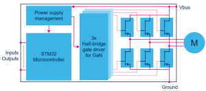 Simplified block diagram of a power inverter based on GaN transistors
Fueling the next generation of motor inverters
GaN is promising important benefits even in applications operating at low frequencies (up to 20kHz). In the realm of home appliances, motor-driven systems such as washing machines, refrigerators, air conditioners, and vacuum cleaners rely heavily on motor inverters to control speed, torque, and efficiency. Unlike industrial servo or precision motors, the physical size of these motors is largely fixed due to mechanical and functional constraints. This means that the traditional approach of reducing overall system size by shrinking the motor itself is not feasible. Instead, improvements must be sought in the inverter and power electronics that drive these motors.
In this sense, it is important to point out that the benefit of GaN over traditional silicon transistors does not come from a single parameter that stands out. It is rather the sum of different aspects concatenating together.
GaN has a de facto negligible reverse recovery charge (Qrr) and low parasitic capacitances, which in turn enable working with slightly higher dV/dt. While the motor winding and insulation limit the maximum allowable dV/dt, GaN’s capability to operate at higher switching speeds allows designers to optimise switching edges carefully.
Moreover, a safe and drastic reduction of dead-time is also achievable without risking shoot-through faults. Time between high-side and low-side switching can be easily lowered by a factor of 10. This can improve inverter efficiency and reduce switching losses without compromising motor reliability.
As remarkable as it gets, the performance is not over yet. In fact, all these “little” improvements combined lead to what may be considered the most relevant of them all: the removal of the heatsink.
Kiss your heatsink goodbye
The considerable reduction in power dissipation allows designers to reduce or even remove bulky heatsinks in the inverter power stage. The assembly line may now require fewer steps in the manufacturing process. No heatsink also means no screws or mounting joints, thus avoiding mechanical failures that can appear when the appliance is already long in the field. An interesting potential saving of service and warranty costs.
The overall result is a more compact, lightweight, and cost-effective inverter design that fits better within the demanding and highly competitive space of the home appliances market.
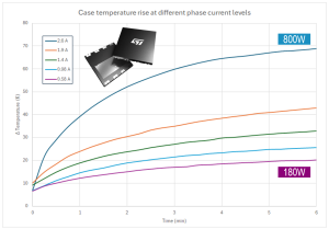 700 V GaN mounted on a motor inverter running without a heatsink
The waveforms show how smooth and cold a GaN can be. In the example above, the device under test has a typical RDS(on) of 80mΩ. The motor inverter runs at a switching frequency of 16 kHz, with a maximum dV/dt slightly under 10V/ns.
A power level of about 800 W can be safely achieved without incurring thermal runaway. The increase in temperature Δt is less than 70 °C, which leaves a good margin before reaching the maximum operating junction temperature (TJmax) of 150 °C.
This remarkable result is achieved without a heatsink, with GaNs mounted on and cooled down through a common 2-layer PCB.
STPOWER GaN Transistors
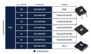
STPOWER GaN Transistors are intrinsically normally off, p-GaN gate e-mode transistors that offer a zero reverse recovery charge. ST offers today seven part numbers rated 700 V breakdown voltage (VDS), with typical on-resistance RDS(on) ranging from 270 mΩ down to 53 mΩ in DPAK, PowerFLAT 8×8, and TO-LL packages.
The portfolio is rapidly growing, adding on different packages, RDS(on) and breakdown voltage levels.
The post GaN Benefits in Motor Controls appeared first on ELE Times.
Union Minister Ashwini Vaishnaw inaugurates TI’s new, world-class R&D centre
Texas Instruments (TI) officially opened its new, state-of-the-art product research and development (R&D) centre in Bengaluru at an event commemorating the company’s 40-year presence in India. As the first multinational company to establish an R&D centre in India in 1985, TI has been instrumental in shaping India’s semiconductor landscape for four decades. The new 550,000-square-foot centre features a collaborative workspace dedicated to developing world-class chip designs. The centre includes an end-to-end reliability lab equipped with advanced testing capabilities for various environmental conditions, along with many other integrated circuit design labs.
Inaugurated by Shri Ashwini Vaishnaw, Union Minister for Railways, Information & Broadcasting, Electronics & Information Technology, Government of India, alongside TI leaders, the new centre highlights the company’s strategic vision to propel semiconductor innovation and nurture world-class design talent. This expansion reinforces TI’s commitment to developing breakthrough analogue and embedded processing technologies while strengthening its support for the design ecosystem and its growing customer base in India.
Shri Ashwini Vaishnaw, Union Minister for Railways, Information & Broadcasting; Electronics & Information Technology, Government of India, said, “I congratulate Texas Instruments on the inauguration of this world-class R&D centre in Bengaluru. TI has been a true pioneer in India’s semiconductor journey and stood as a testament to consistently nurturing the design talent ecosystem in India. The company’s expanded investment reinforces India’s position as a global hub for semiconductor design, development and supports our vision of building an innovation-led nation.”
Santhosh Kumar, president and managing director, TI India, said, “As we celebrate 40 years in India, this milestone reflects TI’s rich legacy and our strong commitment to the future. TI India’s product development and design teams drive research and breakthrough innovations for customers worldwide. Our world-class engineers are central to pioneering the next generation of semiconductor advancements.”
The company recently opened an additional sales office to strengthen its partnership with Indian customers, while the new R&D facility builds on its innovation capabilities in the region. With thousands of employees in India, TI continues to expand its presence in the region.
The post Union Minister Ashwini Vaishnaw inaugurates TI’s new, world-class R&D centre appeared first on ELE Times.
My first project NE555
 | Designd my own PCB and got it from JLCPCB. Nice gift fir valentines. I am using NE555 to make the LEDs flash if you want to see how it works comment I'll post a video. [link] [comments] |
Veeco stockholders approve merger with Axcelis
Texas Semiconductor Innovation Fund grants Coherent $14m to accelerate scaled production of InP wafers
Bridging the design-to-deployment gap: How India can lead the next wave of connected device innovation
Hareesh Ramana, Chief Experience Officer, Sasken Group & President, Borqs Technologies (a Sasken Group company)
India is making significant strides in electronics manufacturing with the aim of 38% value addition within five years. The device manufacturing ecosystem has grown to a significant scale, but it still depends heavily on designs and reference architectures developed elsewhere.
Building domestic capability in electronic device design, especially IoT/connected device design, is critical to India’s ambition of becoming a major electronics manufacturing hub. India’s ambition to reach 38% value addition in electronics manufacturing will be driven not only by scaling assembly but by strengthening device design and systems engineering, which can contribute as much as 30-35% of the total value creation.
Need for in-house design capabilities:
A growing model in India’s connected-device ecosystem is design-led, end-to-end IoT product development anchored locally, covering silicon integration, embedded software, connectivity stacks, and certification. Companies like Borqs Technologies (now part of the Sasken Group) exemplify this approach, offering full-stack IoT design capabilities from within India. For OEMs, this can shorten development cycles, improve control over system integration, and reduce dependence on externally sourced IP and engineering capacity, especially in critical connectivity and compliance stages. Expanding these capabilities across the industry can help India move beyond contract manufacturing and toward the higher-value innovation layer where devices connect to data, analytics, and services.
Time to market gap:
Many IoT projects stall because hardware, firmware, cloud platforms, connectivity, and certification are handled by separate vendors with misaligned priorities.
Over the past decade, India’s product development ecosystem has matured to address these challenges, evolving from a cost-centric outsourcing base into a design-led innovation hub. Global OEMs and platform companies increasingly view India as a partner for rapid prototyping and co-innovation, not just low-cost assembly. Several end-to-end product engineering companies in India exemplify this shift by delivering integrated IoT solutions that shorten development cycles and align with global OEM roadmaps.
Integration as a strategic capability
Connected devices are no longer standalone products; they are endpoints of digital services. The differentiator is therefore systems integration across silicon, hardware, software, connectivity, and lifecycle management. A unified, end-to-end engineering model can enable:
- Faster debugging by tightening the feedback loop between hardware and software teams
- Fewer integration issues by reducing handoffs across multiple vendors
- Quicker prototyping and validation through coordinated design and test cycles
- More predictable certification and production ramp by planning compliance and manufacturability early
- A single accountable partner from concept through delivery and lifecycle management
This is particularly vital for industrial-grade devices where reliability, security, and compliance define adoption. Indian engineering firms with cross-layer capabilities are increasingly enabling platform-driven approaches that allow module reuse across verticals like automotive, energy management, and logistics.
AI and advanced technologies and product development:
Advanced technologies like AI, IoT, automation, digital twins, and cloud computing are transforming product development. AI-driven analytics reduce manual testing cycles, while digital twins simulate device behaviour under real-world conditions, enabling faster iteration and higher reliability.
Demand for software-defined vehicles, smart energy infrastructure, automated factories, and connected appliances is accelerating globally. Multinationals are expanding design centres and co-innovation programs in India to build products for both developed and emerging markets.
For India, the opportunity lies in moving beyond contract manufacturing to the high-value layer where devices meet data, analytics, and services. Mastery over sensors, edge intelligence, connectivity stacks, and lifecycle platforms can enable the country to capture a far greater share of the global electronics economy.
The coming decade will reward ecosystems that can bridge the design-to-deployment gap with reliability and speed. India has the talent, digital infrastructure, and entrepreneurial energy to lead this shift. The next step is an integrated approach that unites design, engineering, and manufacturing into a single innovation continuum.
The post Bridging the design-to-deployment gap: How India can lead the next wave of connected device innovation appeared first on ELE Times.
Found this old relic at my grandfathers house.
 | No idea what this is. Not even sure what it does. Just showing it around. [link] [comments] |
My first Project - Healthtracker
 | Hi everyone, This is my Healthtracker project. This will be my first real 6-Layer PCB I have designed using EasyEDA. I am using the nrf5340 for this low Power Bluetooth application paired with couple i2c peripherals for activitiy, heartrate, time & temp. So I don't run out of storage, I integrated infineon 8-Mbit FRAM. Power is supplied to various DC/DC Buck/Boost converters found at the top. I am planning to programm the SoC using the pinheaders and my DevKit. (pinheaders will be soldered out, after programming and Debugging). Oh, don't be confused with these many throughhole vias; JLCPCB curently doesn't support blind or buried vias.... Have a great day. [link] [comments] |
Сторінки


![[link]](https://i.redd.it/580ajrtzlhig1.png)
![[link]](https://i.redd.it/0klw6posrfig1.png)