


Збирач потоків
Apple’s processor cadence: A pending stutter-step for improved long-term edge inference?

Apple Silicon’s success track record is indisputably impressive. It’s also rife with implementation inconsistency, albeit reflective in no small part of broader industry status impermanence.
When Apple announced its computing platform migration from Intel x86 to homegrown Arm-based SoCs beginning in mid-2020, initial industry response was initially mixed. There was no shortage of schadenfreude, mind you, both considering that Intel had done the same thing to the IBM/Motorola PowerPC Alliance a decade and a half earlier, and more broadly Intel’s then-status as the predominant processor supplier to the computing segment. That said, and as was hopefully evident even in my earliest Apple Silicon era coverage, I was personally confident in the strategy’s sooner-or-later transition success, which is ironically winding up as we speak.
For one thing, Apple’s relationship with Intel was growing increasingly strained, as the chip supplier’s power consumption vs performance trends grew more worrisome, as new-product schedules slipped, and as the bugs in those products multiplied. For another, Apple and foundry partner TSMC (superseding initial partner Samsung) had for a while already been developing new SoCs for smartphones, tablets, smart watches and other devices. And then there’s Apple’s in-house vertical integration and control of both hardware and software, the latter spanning both operating systems and first-party applications and suites, as well as its exclusivity as provider of both developer tools and App Store approvals for third-party coders.
New life
And so here we are with today’s M6, the company’s latest mainstream SoC offering. It’s notable for being the premiere volume production implementation of TSMC’s newest 2 nm fabrication technology foundation. And Apple’s done (as well as, equally notably, not done) numerous things, most of them predictable but a few more surprising, with the expanded (albeit more expensive) transistor budget it’s been foundry-afforded.
The M5, introduced last October, integrated 10 (max, “binned” to fewer than this in some product proliferations to maximize yield and minimize cost) CPU cores and the same 10 (again, max, and again, binned in some variants) GPU cores. Each GPU core also integrated a Neural Accelerator, a fancy name for what’s likely “just” (I jest) a general-purpose massively SIMD revamp of the graphics architecture for enhanced function flexibility. And then there was the standalone 16-core Neural Engine for optimal, albeit function-specific, inference processing.
And the M6? 12 (max, bin-dependent) CPU cores this time: two “super”, four “performance” and six “efficiency”. Clock speeds, no surprise, aren’t public, nor are cache sizes or other important-to-engineer characteristics. 12 (max, again) GPU cores this time, too. And two 16-core Neural Engines. The AI emphasis is obvious, yes? And what about performance? Apple claims “up to 1.2x faster multithreaded performance as compared to M5,” which is to some degree to be expected due to the greater CPU core count, although more than a straight linear interpolation would be expected to deliver. And single-threaded improvements? I thought you’d never ask…and some part of me wishes you wouldn’t have asked, because the answer is so very lame. “It delivers the world’s fastest single-threaded performance.” That’s it. Seriously, Apple?
Life extension
What about the M5 family; is it drifting off the stage as the M6-series successors take their turn in the spotlight? Not quite…and maybe not for a while yet (hold that thought). Apple just introduced the M5 Ultra SoC, combining two M5 Max die via a silicon interposer “stitching” technology the company brands as UltraFusion. Here’s the twist…the M5 Max itself, as I wrote about in March, is a dual-die UltraFusion-stitched configuration, as is its M5 Pro enabled-core-count subset. So, what we have here is Apple’s first quad-die, UltraFusion-combined design.
This all leads back to the “implementation inconsistency” allusion in the upfront subhead of this writeup. The first-generation Apple Silicon M1 family die shots are shown at the beginning of this section. The M1, along with the M1 Pro and M1 Max, were all single-die designs, albeit (as you can see if you look closely) with the die area devoted to the M1 Max’s graphics subsystem effectively implemented as a mirror-image doubling of that in the M1 Pro. But the M1 Ultra, unveiled ~1.5 years after the M1, employed UltraFusion dual-die merge for the first time.
Apple has skipped the “Ultra” tier for both the M2 and M4 generations; this is the first time we’ve seen one since the M3 series, where the baseline, Pro and Max tiers were simultaneously unveiled, all in single-die form, and with the M3 Ultra once again arriving 1.5 years later as a dual-die stitched design. This time around we’ve got, adding together the innate resources of each of the four dice, an up-to-36-core CPU consisting of 12 super cores and 24 performance cores, and a next-generation GPU as many as 80 cores. Compared to the M3 Ultra, Apple claims that the M5 Ultra’s CPU subsystem delivers up to 1.25x higher single-threaded performance and up to 1.3x higher multithreaded performance, with the GPU cluster supplying up to 4.5x the peak GPU compute for AI. Note, again, the AI emphasis, as if it was even possible to miss!.
Price explosionThe first systems containing these new chips are, for the M6 (and already introduced, but first-time in this form factor, M5 Pro), the Mac mini.

And for the M5 Ultra (and already introduced, but first-time in this form factor, M5 Max), the Mac Studio.

The key aspect of these parts of the story is, unsurprisingly, memory—DRAM for system and unified graphics and flash memory for the SSD—and their impacts on pricing versus with prior-generation systems in less supply-constrained times. The case study example in one of John Gruber’s event coverage posts tells, I think, the tale best of all.
If you configure an M6 Mac Mini with 2 TB of storage, the SSD upgrade ($1,000) costs more than the entire base model computer ($900). So too with the 4 TB SSD upgrade for the M5 Pro Mini ($1,800 upgrade for a $1,700 computer).
I’ll also posit a question: why did Apple make this announcement now, particularly given that initial system configurations won’t start shipping until late next month, with higher-end follow-on tiers not available until (at least) October? The company is widely expected to roll out its next-generation iPhones (high-end variants, at least), smart watches, earbuds and other related (and not?) goodies in just two weeks’ time; why not just unveil everything all at once?
Mebbe Apple’s already got so much already planned for September 9 (I’m guessing) that it decided to split the total tranche into two events out of necessity? Or maybe Intel…or AMD…or Qualcomm…or Nvidia…or some other chip and/or system supplier has something already planned for the near future, and Apple caught wind of it and decided to launch earlier than originally planned (note the lack of a dedicated event today) to steal competitive thunder?
What’s next?
I saved the best for last, IMHO and if the rumors are true. Using past history as a (potential) guide to the future, when will Apple roll out the M6 Pro, Max and maybe even Ultra (though, as already noted, this only seems to happen in odd-number generations) SoCs? How about never?
For many years, although it admittedly still boggles my mind to type these words, we’ve largely in-retrospect learned that Apple apparently was seriously involved in the development of an Apple-branded, battery-powered and autonomous car. The project is now mothballed, with the former test track now owned by Waymo, although its lineage lives on somewhat in Ferrari’s Luce, designed in conjunction with former Apple chief design officer Jony Ive and shown above.
The Apple Car project apparently involved not only vehicle hardware and software development but also dedicated-silicon development, specifically for inference processing. Apple is reportedly now “baking” its inference learnings from those earlier efforts into an accelerated development timeframe for its M7-series (and beyond) SoCs. As such, to the “stutter step” reference in the title, there supposedly won’t be any M6 variants, therefore systems based on them, beyond the baseline chip introduced today (and also encompassing, I’m guessing, pending updates to the 24″ iMac and the MacBook Air).
I’ve long believed, and intend delve into further detail in a near-future dedicated-topic blog post to come, that the long-term winners in AI silicon will be:
- Volatile and nonvolatile memory suppliers, and
- Dedicated-function inference processor and core suppliers
for the same fundamental reason: inference processing largely done today in the “cloud” will inevitably move, at least in part, to the edge. And what better case study for the trend exists than an autonomous vehicle, which absolutely cannot tolerate the lengthy roundtrip processing latency from the vehicle to the cloud and back, assuming it even has reliable connectivity at all?
—Brian Dipert is the associate editor, as well as a contributing editor, at EDN.
Related Content
- Apple’s question for the developer: Are you up for an AI do-over?
- Apple’s spring 2026 soirée: The rest of the story
- Apple’s M5: The SoC-and-systems cadence (sorta) continues to thrive
- The 2025 WWDC: From Intel, Apple’s Nearly Free, and the New Interfaces Are…More Shiny?
- The 2024 WWDC: AI stands for Apple Intelligence, you see…
The post Apple’s processor cadence: A pending stutter-step for improved long-term edge inference? appeared first on EDN.
How to make a simple low voltage dc power and data over 2 wires.
 | submitted by /u/Relevant_Pumpkin9190 [link] [comments] |
Navitas to acquire power management firm Claros
Flexible and Printed Electronics: The Circuits of the Future
3D-Printed Frame for a 32×32 LED Matrix with Microphone
GSM Emergency Call System with RF Receiver for Elderly and Bedridden Patients
Comparing multi-channel RF transceiver options for space applications

Spacechips has been asked by its clients many times, “Which is the best device?” The answer? “It depends”.
Payload manufacturers are increasingly exploiting the SWaP (size, weight, and oower) advantages of single-chip, multi-channel transceivers, combining DSP and AI with RF ADCs and DACs. These devices offer significant benefits and flexibility to satellite operators, allowing them to change receive and transmit frequency plans in-orbit to deliver better services and more insights.
Using systems based on them, telecommunication operators can achieve better link performance, coverage and spectrum efficiency, while earth-observation users can transmit and receive multiple RF bands within the same orbital pass to monitor different terrains and penetration depths using a single transponder. SIGINT/ELINT operators can monitor UHF to K-band using one radio channel. The following example (Figure 1) illustrates C and Ku-band carriers being simultaneously under-sampled at 3 GSPS with respect to their absolute centre frequencies, but over and bandpass sampled in relation to their information bandwidths.

Figure 1 C and Ku-band carriers digitized at 3 GSPS are simultaneously under-sampled with respect to their absolute center frequencies and over- and bandpass-sampled in relation to their information bandwidths. Source: Spacechips
Satellite applications are increasingly processing wider and instantaneously reconfigurable bandwidths to deliver better services and more value-add. As a designer and manufacturer of software-defined transponders, my company Spacechips considers various single-chip transceivers for different customers. These devices enable operators to change, receive and transmit frequency plans, information bandwidths, modulation and waveform types in-orbit, in response to varying communication and traffic needs.
Integrated, multi-channel semiconductors such as the AMD’s (formerly Xilinx’s) RFSoC and Versal RF, Altera’s Agilex Direct RF, Texas Instruments’ AFE80xx, Jariet Technologies’ Elektra and Analog Devices’ AD9082 offer obvious advantages such as smaller size, lower power consumption and in some cases, elimination of the external interfaces between the ADC/DAC and DSP. I remember doing the layout of the first Spacechips SDR1 prototype, where the digital interface between the ADC and the FPGA required fifty impedance- and length-matched traces, as shown in Figure 2.

Figure 2 ADC LVDS digital outputs (left) connected to a FPGA (right) exemplify legacy system design complexity. Source: Spacechips
Over the past near-two decades, transponder architectures have become increasingly software-defined, with traditional, analogue superheterodyne circuits being replaced by digital and re-configurable logic. The latest, single-chip, multi-channel transceivers offer the potential to deliver true software-defined microwave. My company’s (Spacechips) customers constantly ask questions such as the following:
- Which microchip they should use
- How they can improve ADC/DAC performance when directly processing RF carriers
- If parts will function reliably in space, and if they have heritage
- How can the customers implement in-orbit AI and machine learning, and
- How they should they design-in the parts.
There’s a big difference between:
- Evaluating these devices using development kits that accept a ±1V carrier and looking at its idealized output spectrum, and
- Developing a payload baselining the same part, combining RF and high-speed digital, and delivering the advertised SNR and SFDR from a ‑120 dBm input!
Does your test equipment have the sensitivity and RF bandwidth to prove this amplitude, for example? And there’s also a huge disparity between powering a 10 W and a 120 W semiconductor!
Spacechips provides training on, including demonstrating, the aforementioned AMD, Altera, Texas Instruments, Jariet Technologies and Analog Devices parts; in my next series of posts, I’ll share insights and lessons learned. This first tutorial will introduce devices, compare their specifications, and discuss their respective suitability for satellite applications.
Future posts will share design-in experiences and measurement results. And with that all said, discrete, space-grade, broadband ADCs and DACs up to K-band are also available, some of which offer advantages over these devices, e.g. RF bandwidth, reliability, availability, and space-qualified status. I have previously written about some of these latter options.
AMD RFSoC and Versal RFBack in 2017, I first posted about AMD’s first-generation RFSoC product family. Gen. 3 integrates a Zynq UltraScale+ MPSoC with 14-bit, 5 GSPS, 6 GHz ADCs and 14-bit, 10 GSPS, 6 GHz DACs (Figure 3). The DFE variant operates up to 7.125 GHz. The original RFSoC was the first semiconductor device to integrate high-speed mixed-signal convertors with an FPGA and Arm Cortex processors, removing the traditional physical interfaces between these respective technologies.

Figure 3 The RFSoC family combines mixed-signal converters with FPGA fabric and Arm processors. Source: AMD
AMD’s Versal RF improves on RFSoC by offering faster and wider bandwidth mixed-signal converters, i.e. 14-bit, 8/32 GSPS, 18 GHz ADCs and 14-bit, 16 GSPS, 18 GHz DACs (Figure 4). The Versal ACAP product range contains dedicated AI engines with vector processors to accelerate machine learning, and AMD plans to formally qualify two devices from the new Versal RF product family: the VR1602 and VR1652 parts.


Figure 4 The Versal RF product family comes in multiple device options with varying ADC and DAC counts and types. Source: AMD
Conceptually, Altera’s Agilex 9 Direct RF family is similar to RFSoC, but it offers faster and wider-RF bandwidth mixed-signal converters enabling millimeter-wave sensing payloads, i.e. 10-bit, 64 GSPS, 36 GHz ADCs and 10-bit, 64 GSPS, 36 GHz DACs (Figure 5). Higher sampling frequencies enable the digitization and synthesis of wider instantaneous information bandwidths. A lower bandwidth, higher dynamic performance, sixteen channel, 14-bit, 4 GSPS, 7.1 GHz ADC and 14-bit, 12 GSPS, 7.1 GHz DAC version is also available. The Agilex 9 Direct RF FPGA contains robust tensor-capable DSP blocks within its fabric to support SIMD execution to accelerate AI operations.

Figure 5 The Agilex 9 Direct RF FPGA integrates tensor-capable DSP blocks within its programmable fabric. Source: Altera
Texas Instruments’ AFE80xx is an integrated RF transceiver offering 14-bit, 4 GSPS, 7.1 GHz ADCs and 14-bit, 12 GSPS, 7.1 GHz DACs (Figure 6). The AFE80xx has eight JESD204B/C serial interfaces to connect to an ASIC or an FPGA at speeds up to 32.5 Gbps per lane. The AFE8010 variant is a ten-channel receiver-only device.

Figure 6 This AFE80xx functional block diagram shows the device’s sizeable single-chip functional integration. Source: Texas Instruments
Jariet Technologies offers the Electra-MA/MK/MX dual-channel transceivers containing two 10-bit, 40 to 64 GSPS ADCs and DACs processing instantaneous bandwidths of 6.4 GHz up to 36 GHz (Figure 7). Elektra devices have sixteen JESD204B/C interfaces to connect to an ASIC or an FPGA at speeds up to 30 Gbps per lane.

Figure 7 Elektra devices’ JESD204B/C interfaces connect to an ASIC or an FPGA at speeds up to 30 Gbps per lane. Source: Jariet Technologies
Analog Devices’ AD9082 integrates two, 12-bit, 6 GSPS, 8 GHz ADCs and four 16-bit, 12 GSPS, 8 GHz DACs (Figure 8). The AD9082 has sixteen JESD204B/C interfaces to connect to an ASIC or an FPGA at speeds up to 24.75 Gbps per lane.

Figure 8 The AD9082 integrates multiple high-precision, high-performance ADCs and DACs. Source: Analog Devices
As noted earlier, Spacechips has been asked many times, “Which is the best device?” Some of our clients need to perform a lot of real-time DSP and/or AI inference on the incoming carrier traffic, so a Versal RF or an Agilex 9 Direct RF may be a better fit for their application. However, several of our other customers do not fit this same definition, and a large, complex, highly-integrated device requiring lots of power rails and watts is therefore likely not their optimum solution.
Two of our clients need more dynamic performance than that offered by ten-bit ADCs/DACs, and exploiting the processing gain from over-sampling is one way to deliver higher SNR. Many users complain about not achieving the advertised data sheet performance and we therefore teach them how to extract every last dB of performance from these parts. Just because a device has a specified sampling/reconstruction clock frequency of Fs GSPS, this does not always result in an information bandwidth close to theoretical Nyquist, i.e. Fs/2 Hz.
For some of our customers, there are financial and programmatic reasons that influence which part to baseline. One of our primary clients, for example, requires a year to approve a new supplier. This timeline did not fit with the project schedule and they resultantly developed an expensive, over-engineered system (in my opinion). For some of our clients, the physical size and/or power consumption of an integrated transceiver may be prohibitive, e.g. a 1U COTS payload might not have an adequate area or financial budget, and its small platform may not be able to generate sufficient energy to supply a power-hungry device.
Other integrated transceivers also exist, of course, but I focus here on the ones that are of most interest to Spacechips and our customers. Most of the devices are part of a wider product suite offering varying numbers of channels, resolutions and sampling speeds. Table 1 summarizes the basic specifications of the six devices and families discussed here.
|
|
RFSoC |
Versal RF |
Direct RF |
AFE80xx |
Elektra |
AD9082 |
|
Architecture |
FPGA, Arm, RX/TX |
FPGA, Arm, RX/TX |
FPGA, Arm, RX/TX |
RX/TX, ADC & DAC |
RX/TX, ADC & DAC |
RX/TX, ADC & DAC |
|
Technology Node |
16 nm FinFET |
7 nm FinEFT |
10 nm SuperFin |
16 nm FinFET |
12nm CMOS |
28nm CMOS |
|
Integrated FPGA |
Yes |
Yes |
Yes |
No |
No |
No |
|
ADC Resolution |
14-bit |
14-bit |
10-bit |
14-bit |
10-bit |
12-bit |
|
Maximum ADC Sampling Rate |
5 GSPS |
32 GSPS |
64 GSPS |
4 GSPS |
40 to 64 GSPS |
6 GSPS |
|
ADC RF Bandwidth |
6 GHz |
~18 GHz |
36 GHz |
7.1 GHz |
36 GHz |
8 GHz |
|
DAC Resolution |
14-bit |
14-bit |
10-bit |
14-bit |
10-bit |
16-bit |
|
Maximum DAC Sampling Rate |
10 GSPS |
16 GSPS |
64 GSPS |
12 GSPS |
40 to 64 GSPS |
12 GSPS |
|
DAC RF Bandwidth |
6 GHz |
~18 GHz |
36 GHz |
7.1 GHz |
36 GHz |
8 GHz |
|
Maximum Instantaneous Bandwidth |
~2 to 4 GHz |
~16 GHz |
> 20 GHz |
0.4 to 1.2 GHz |
6.4 GHz |
~4 to 8 GHz |
|
AI Acceleration |
Fabric |
AI Engines |
Tensor Fabric |
No |
No |
No |
Table 1 A comparison of device specifications covers the companies and products discussed in this blog post. Source: Spacechips
All of the parts discussed here contain integrated DDCs and DUCs to assist with carrier digitization and synthesis, respectively, as well as re-programmability. For fixed frequency plans, bandpass carriers can be directly under-sampled and aliased into the baseband zone (Figure 1). For example, for a 64 GSPS ADC, a 400 MHz-wide signal centered at 25 GHz can be digitized at 1 GSPS (bandwidth over-sampling of 2.5). For wider-band carriers, e.g. SIGINT spectrum monitoring or SATCOM gateways, you do not need to decide beforehand which signal you want; you can digitize the complete Nyquist bandwidth and, using software DDC control, gain, filter and decimate the required signals.
Some of the devices contain multiple independent DDCs to extract separate baseband streams. Decimation lowers the sample rate supplying the FPGA with data, at 1 GSPS versus 64 GSPS as in the above example, reducing memory bandwidth and easing FPGA resource utilization. For CMOS devices, a lower switching speed also reduces power consumption.
On the transmitting side, some of the DACs can directly up-convert baseband to IF/RF images in the higher Nyquist zones, as illustrated in the following example with an update rate of 10 GSPS (FIgure 9). Similarly for wider-band carriers, a DUC can significantly reduce the data bandwidth to the FPGA, interpolating, up-converting, removing unwanted images and flattening the sinc roll-off within the desired passband. Changing frequency plans requires reprogramming the NCO rather than altering the entire analog RF chain.

Figure 9 This graphic shows C and Ku-band carriers in the first and fourth Nyquist zones. Source: Spacechips
None of the parts discussed here were developed specifically for space applications, but several are currently operating in-orbit. All are fabricated using ultra-deep-submicron geometries, e.g. 16 or 7 nm FinFET, 10 nm SuperFin or 28 or 12 nm CMOS, and their thinner oxide as well as general scaling have made them intrinsically tolerant to total-dose changes over the lifetime of a mission. Several also contain process-level radiation-hardening to eliminate single-event latch-up.
Device-level mitigation, e.g. the use of EDAC within fabric memory and triplicated HDL, as well as system techniques, e.g. power-rail monitors, have collectively improved overall reliability sufficiently for certain customers, resulting in very enabling transponder designs. Some of the devices have been irradiated and several are currently being tested in-beam.
ConclusionsMy next planned article will describe using, testing and designing-in the devices discussed here, all of which have unique requirements. Please note that the company and product names contained within this writeup are copyrighted and trademarked by their owners!
I’m off to the lab begin testing several the first of the parts. Until next time, the person who shares their best integrated transceiver design-in story in the comments below will win a Spacechips’ Training World Tour tee-shirt. Our global training schedule can be viewed at our website (www.spacechips.co.uk/training_courses), or email us (events@spacechipsllc.com) for more information.
Dr. Rajan Bedi is the CEO and founder of Spacechips, which designs and builds a range of advanced, AI-enabled, re-configurable, L to K-band, ultra high-throughput transponders, SDRs, Edge-based on-board processors and Mass-Memory Units for telecommunication, Earth-Observation, ISAM, SIGINT, navigation, 5G, internet and M2M/IoT satellites. The company also offers Space-Electronics Design-Consultancy, Avionics Testing, Technical-Marketing, Business-Intelligence and Training Services. (www.spacechips.co.uk).
Related Content
The post Comparing multi-channel RF transceiver options for space applications appeared first on EDN.
Hardware security verification must go beyond functional testing

Imagine you’re an attacker staring at a billion-transistor system-on-chip (SoC). You don’t care whether the design boots Linux, passes simulation, or meets its performance targets. Your objective is far simpler. Find the one flaw nobody thought to look for.
It might be an undocumented debug port or path. Maybe it’s a configuration error between hardware and firmware. Sometimes it’s a perfectly legitimate sequence of operations that exposes sensitive information in a way the original team never anticipated. A single overlooked weakness is all it takes.

This is why testing for unexpected data paths is crucial. Source: Arteris
Design teams focus on proving that a chip operates according to its intended specifications. Security assurance requires answering a different set of questions to identify the conditions that could violate security objectives. As the above figure illustrates, security verification must test for unexpected data paths that could expose sensitive information, not only confirm that intended paths operate correctly.
Beyond intended behavior
Security verification starts from a different premise. The concern is not whether a protected asset reaches the encryption engine, but whether information associated with that asset can reach an unauthorized destination. A debug interface may unintentionally expose sensitive information, or firmware may fail to clear a memory location after a key has been used. Otherwise, legitimate operations can also interact to create an unexpected path through the system.
Achieving that level of assurance requires security requirements that can be verified throughout the design, measured for coverage, and evaluated across complex hardware-firmware interactions. Those requirements provide the basis for determining whether security objectives continue to hold as the complete system evolves.
Functional security verification evaluates whether a design matches its specification. Engineers derive tests from defined requirements and use them to demonstrate that data, control signals, and system transactions occur as designed.
For example, testing can confirm that an encryption block obtains a key from memory, receives it within the required timing constraints, and completes the requested operation successfully. Those results establish functional correctness, but they do not by themselves address unintended information paths or residual sensitive state.
Find the weakness, not the exploit
One of the biggest misconceptions in hardware security is that engineers should focus on finding vulnerabilities, which rarely manifest as a single, obvious flaw. On the other hand, a weakness is an underlying design condition that can allow security protections to be circumvented, creating multiple opportunities for exploitation in complex designs.
That is why security verification begins by identifying weaknesses rather than individual security exposures. By addressing the underlying conditions, security teams can eliminate entire categories of exposure, reducing risk far more efficiently.
Security weaknesses often emerge through interactions among hardware blocks, firmware, and system configuration. A block-level functional test may confirm that temporary storage holding a cryptographic key is cleared when commanded. After integration, however, firmware may omit or mistime the command, leaving the key resident longer than intended. The block passes in isolation, but the integrated system violates the security objective.
Rather than creating a separate test for every possible vulnerability, a more effective approach is to define the security condition that must hold. A cryptographic key should be cleared when it’s no longer needed. It should never reach an unauthorized block or cross a security boundary except under explicitly approved conditions. Verification then determines whether that condition holds throughout the design.
Information flow at system scale
Information-flow analysis traces critical design assets across a chip as the values carrying their information pass through logical and sequential transformations or intermediate storage locations. Rather than checking only for an expected value at a specified point, the method preserves traceability over time even when the original value no longer appears intact. This visibility helps reveal leakage paths and unexpected security behavior.
Security rules used in simulation at the block and subsystem levels can be carried into emulation for full-SoC hardware, firmware, and software verification. This scalable, repeatable approach also supports third-party IP assurance across the design supply chain. A security monitor generated for a component can then be reverified at the full-chip level, providing evidence that security requirements remain satisfied through integration and configuration.
Security coverage
Security coverage answers a basic question about whether the design was tested well enough. For each security rule, the metric indicates how thoroughly the existing test suite exercised the relevant logic. A passing result carries limited weight when that activity was minimal. The analysis can locate RTL that has not been exercised sufficiently and direct additional testing to those areas.
The resulting data allows teams to track progress and make informed decisions. Coverage does not turn dynamic analysis into exhaustive proof. It shows how much evidence supports signoff and where gaps remain. As regulatory requirements and customer expectations continue to increase, teams need objective evidence of what was verified.
A different way to think about verification
The semiconductor industry has become exceptionally good at proving that designs work. So, the next step is to verify that security objectives are maintained under most relevant conditions. That requires a shift in mindset, from relying on assumptions to defining security requirements, verifying them, and measuring coverage.
Take, for instance, Cycuity, which provides the software needed to put this methodology into practice. The Cycuity Radix platform integrates with existing simulation and emulation environments, allowing teams to verify security requirements, detect security violations, and measure coverage as part of their normal verification flow. Cycuity Radix-S supports simulation-based verification, while Cycuity Radix-M extends the approach to emulation, helping teams evaluate security at full-chip scale.
Security verification is its own discipline, one that must go beyond functional testing to assess whether security objectives are maintained across the integrated system.
 John Elliott is a security applications engineer at Arteris, bringing over 35 years of experience in electronic design automation (EDA). His work centers on security assurance for hardware designs, helping designers identify and mitigate security vulnerabilities in semiconductor devices before they are manufactured.
Related Content
- IoT security: Challenges and solutions
- Torture-testing your new SoC’s security quotient
- Hardware Root of Trust Essential for AI Chip Integrity
- Lockdown! Random Numbers Secure Network SoC Designs
- Hardware Security Requirements for Embedded Encryption Key Storage
The post Hardware security verification must go beyond functional testing appeared first on EDN.
Infineon Acquires C2i Semiconductors to Expand its Innovation Capabilities in AI Data Center Power Management Solutions
Infineon Technologies AG today announced the acquisition of C2i Semiconductors, a Bangalore-based technology company specializing in software-defined multiphase controllers and smart power stages for AI data center applications. C2i Semiconductors’ technology complements Infineon’s leading portfolio of power semiconductors and power systems, enabling intelligent and scalable power delivery architectures from grid to core for AI servers and high-performance computing platforms. The acquisition further strengthens Infineon’s top position in power solutions for AI data centers while expanding its engineering capabilities in India and reinforcing the country’s role as a strategic innovation hub. The transaction is expected to close in the third quarter of calendar year 2026.
“This acquisition will further strengthen Infineon’s leadership in power solutions for AI data centers and create a new center of excellence for digital power technologies in India,” said Adam White, President of Infineon’s Power Systems (PS) division. “C2i Semiconductors brings exceptional expertise in software-defined power management and system-level power architectures, backed by a proven highly experienced engineering team with decades of combined industry experience. With this acquisition, we will accelerate innovation in power delivery solutions for AI data centers, expand our capabilities in next-generation vertical power delivery architectures, and create significant value for our customers.”
“We founded C2i Semiconductors with the vision of bringing greater intelligence to power delivery systems and addressing the growing power challenges of AI infrastructure. Joining Infineon gives us access to world-class semiconductor technologies, manufacturing capabilities, and global customer relationships. Together, we can accelerate the development of software-defined power architectures and bring our innovations to customers worldwide,” says Ram Anant, Founder & CEO of C2i Semiconductors.
Software-defined power solutions combine advanced power semiconductors with intelligent digital control and software algorithms to optimize power conversion, regulation and system performance in real time. As increasingly powerful AI processors create highly dynamic and rapidly changing power demands, power delivery systems must respond faster and more precisely to sudden load fluctuations while maintaining efficiency and system stability. By adding intelligence to the power delivery architecture, software-defined solutions help data center operators improve efficiency, reduce power losses, and support the increasing power density requirements of next-generation AI processors. C2i Semiconductors’ technology takes a system-level approach to power delivery, spanning the path from grid to core and enabling more intelligent and adaptive power architectures for AI infrastructure.
The acquisition combines C2i Semiconductors’ digital power expertise with Infineon’s global scale, application know-how and broad portfolio of power semiconductors, including silicon, silicon carbide (SiC) and gallium nitride (GaN) technologies, as well as vertical power delivery solutions, paving the way to future Substrate Integrated Voltage Regulators (SIVR). Together, the companies will accelerate innovation in AI power delivery systems and support the growing performance and efficiency requirements of next-generation AI infrastructure.
In addition, the transaction adds highly specialized expertise in software-defined power management to Infineon’s global R&D network and further strengthens its innovation capabilities in India. Infineon currently employs approximately 2,800 employees in India – one of the world’s most dynamic semiconductor and technology ecosystems.
The post Infineon Acquires C2i Semiconductors to Expand its Innovation Capabilities in AI Data Center Power Management Solutions appeared first on ELE Times.
Wolfspeed’s device revenue rebound driven by AI data center business
India Unveils ₹62,500-Crore Mobile Phone Manufacturing Scheme to Deepen Electronics Localisation
₹62,500 crore Mobile Phone Manufacturing Scheme (MPMS) has been notified by the Government of India in a new policy impetus to accelerate domestic mobile-phone manufacturing, increase local value addition, and firm up the electronics manufacturing in India. Ministry of Electronics and Information Technology (MeitY) has notified the scheme on 21 August 2026 and it is effective from 01 April 2026 for a term of five years to end in FY2030-31.
This fresh programme is set up after the existing Production Linked Incentive (PLI) Scheme for Large Scale Electronics Manufacturing was put into effect in March 2026. Although the previous programme was responsible in placing India as a huge centre of mobile production as well as export, MPMS’ new programme emphasizes more on the domestic value added, on locating the components and developing native mobile brands.
Under the MPMS, eligible mobile-phone makers may avail of incentives from 2.25 per cent to 5 per cent on eligible sales in the relevant category and conditions. The scheme also offers an additional incentive of up to 1.5 per cent for domestic sourcing of certain key components and sub-assemblies. Also, Indian brands are given additional support for product design and R&D, with a 3 per cent incentive on eligible sales as per the relevant scheme guidelines.
In terms of technology and manufacturing, local sourcing is of greater consequence. Increased component localisation would promote investment across printed circuit boards, camera module, display, batteries, mechanical components and other electronic sub-assemblies. This would help shift the Indian electronics industry gradually beyond final assembly towards higher value manufacturing and a stronger local supply chain.
The post India Unveils ₹62,500-Crore Mobile Phone Manufacturing Scheme to Deepen Electronics Localisation appeared first on ELE Times.
India-Japan Business Mission Puts Semiconductors and Electronics Cooperation in Focus
India and Japan are looking to expand collaboration on semiconductor, electronics, and other high-technology industries with the largest ever business delegation to Japan, led by the Union Ministry for Commerce and Industry, Piyush Goyal. More than 200 business members make up the 4-day delegation to the visit that will take place from August 24 to August 27 in the cities of Tokyo, Nagoya, and Osaka.
The visit coincides with a period when India is increasing its domestic capabilities to set up semiconductor manufacturing facilities and electronic value chains, while Japan is a leading global source of semiconductor inputs, equipment, and technology. FICCI is organising the business mission to explore new opportunities for cooperation in high-technology and cutting-edge sectors, including semiconductors and electronics. FICCI Director General Jyoti Vij said that the organisation expects several Memoranda of Understanding (MoUs) to be signed during the visit.
The delegation includes representatives from a diverse number of sectors-ranging from manufacturing to semiconductors to clean energy and steel to automotive, financial services, healthcare and start-ups. The program is expected to encompass over 200 business-to-business meetings, dedicated networking sessions and about 15 site visits, providing platforms for Indian and Japanese firms to pursue possibilities for investment and technical and supply chain collaboration.
Far from an expansion of India-Japan trade alone, the business mission, particularly focusing on semiconductors and electronics, can also lead to a new phase of opportunities for tech transfer, industrial investment and new supply chain arrangements.
The post India-Japan Business Mission Puts Semiconductors and Electronics Cooperation in Focus appeared first on ELE Times.
JSW Centre of Excellence in Smart Grid and Automation Launched at MSRIT
The JSW Centre of Excellence (CoE) in Smart Grid and Automation was formally launched at MS Ramaiah Institute of Technology (MSRIT) Bengaluru, marking a significant step towards strengthening India’s power infrastructure for the renewable energy era.
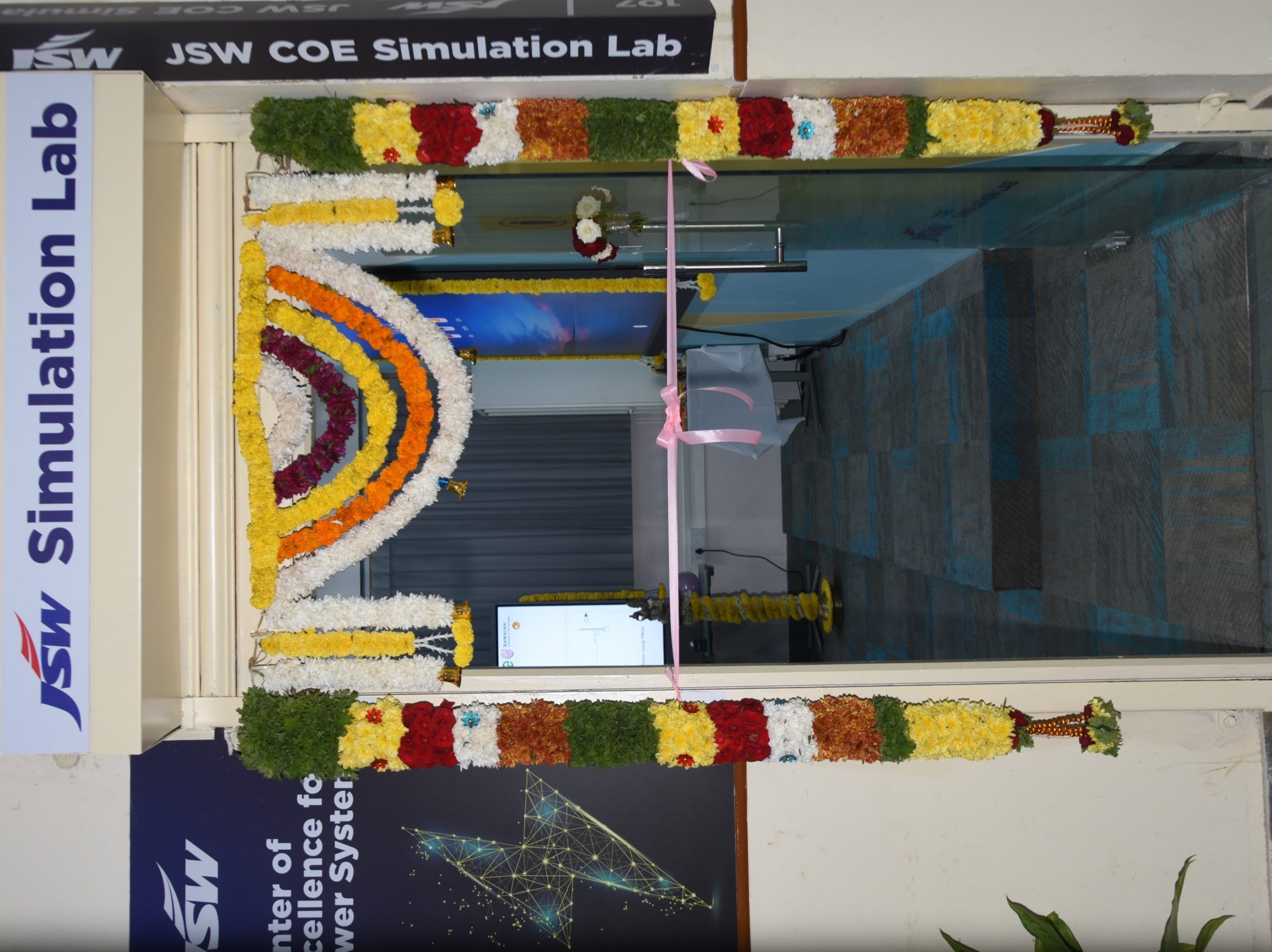
The JSW-CoE has been jointly established by JSW Group, Sharika Enterprises and MSRIT to address one of the most pressing challenges in the power sector today-maintaining grid stability amid the rapid growth of renewable energy.
India has made remarkable progress in adding solar, wind and Battery Storage Systems (BeSS). However, renewable energy brings variability and uncertainty that traditional grid systems were not originally designed to handle. This has created a gap between renewable energy generation, grid stability and market participation. The JSW-CoE has been set up with a clear purpose to bridge this gap through advanced system modelling, automation, analytics and real-time simulation.
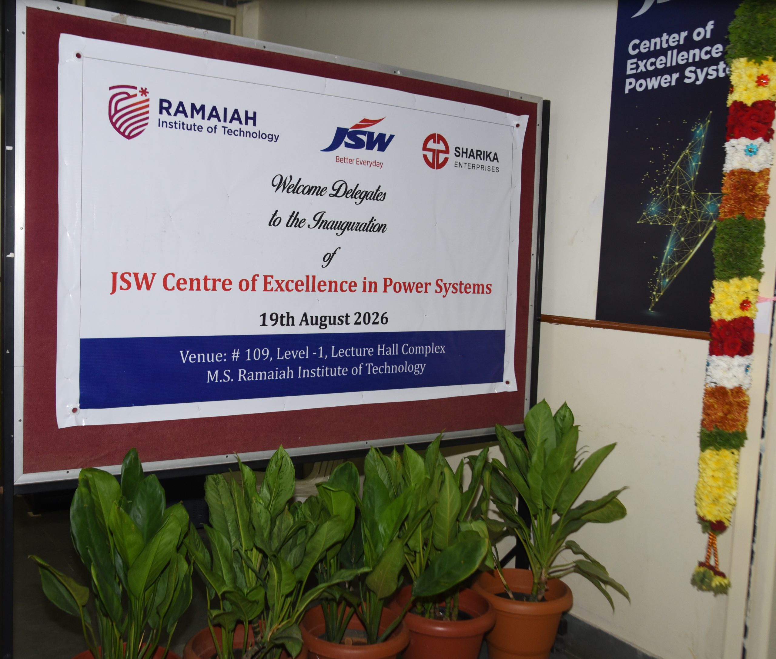
As per National smart grid mission under RDSS GOI has to establish several Centre of excellence in flexible power system across country to enhance capabilities in advanced power management practices to enhance operational efficiency and sustainability across our RE aggregation ecosystems. This Centre of Excellence in Power Systems reflects the commitment to strengthening the national grid infrastructure at a critical time. As renewable energy capacity grows, grid systems must become smarter, more stable and more market-ready. This initiative aims to support innovation, industry collaboration and the development of skilled professionals who can manage the complex power systems of the future.
The JSW-CoE operates on a unique Lab-as-a-Service model. JSW Group has funded the capital investment required to establish the advanced laboratory infrastructure. Sharika Enterprises has designed, set up and will manage the operations of the lab, drawing on its deep expertise in power automation, protection systems, Supervisory Control and Data Acquisition (SCADA) and international communication protocols such as IEC 61850 and IEC 60870. MSRIT hosts the JSW-CoE and provides the academic ecosystem to support research, certification and long-term skill development. The JSW-CoE has been structured as a non-profit entity, with a clear focus on capability building rather than commercial returns.
Mr. Rajinder Kaul, Chairman and Managing Director, Sharika Enterprises, said, “The power sector is undergoing a structural transformation. Utilities, renewable developers and system operators need access to real-world testing environments before deploying solutions in the field. This Centre has a capability to simulate a complete power system within a controlled lab environment, enabling stakeholders to simulate grid conditions, test automation solutions and prepare for market participation. Our goal is to build both technology readiness and human capability for the smart grids of tomorrow.”
The facility is designed to replicate generation, transmission and distribution systems in an integrated setup. It includes SCADA and dispatcher systems, renewable energy management platforms, PMU-based protection and wide-area monitoring and tools for real-time load flow studies, contingency analysis and energy market simulations. Industry players, startups, utilities and researchers can access the lab at a reasonable cost to test systems, validate solutions and prepare for deployment.
Convergence of academia and industry:
Beyond technology development, the Centre will focus strongly on skill building. Engineers of the future must understand power systems, communication protocols, real-time data management, automation, artificial intelligence and energy trading mechanisms. Through masters, certification courses and industry-linked projects, the JSW-CoE aims to create a pipeline of professionals equipped for India’s evolving power landscape.
Lauding the JSW-CoE, Dr. N V R Naidu, Principal, MS Ramaiah Institute of Technology, said, “The launch of the JSW-CoE at MSRIT represents a powerful convergence of academia and industry. As the power sector evolves with renewable integration and digital technologies, it is essential that our students and researchers gain hands-on exposure to real-world grid systems, automation platforms and advanced simulation environments. This collaboration will enable MSRIT to nurture the next generation of engineers who can contribute meaningfully to India’s smart grid and energy transition journey.”
The launch of the JSW-CoE positions Bengaluru as a growing hub for smart grid innovation and advanced power system research. By bringing together industry investment, academic strength and technical expertise, the initiative seeks to support India’s long-term power transition and ensure that renewable growth is matched by grid intelligence and market readiness.
The post JSW Centre of Excellence in Smart Grid and Automation Launched at MSRIT appeared first on ELE Times.
Ground broken on Alcoa-Sojitz Gallium Recovery Project in Western Australia
The Steam Deck has 3 PCBs per trackpad
 | submitted by /u/K0eg [link] [comments] |
Quintessent raises $40m in oversubscribed Series A funding round
Mouser website now blocks Linux users
 | Really baffling decision, my last order from them was only a few months ago. Apparently Linux is no longer a "standard" operating system! [link] [comments] |
🎥 У КПІ ім. Ігоря Сікорського урочисто відзначили День Державного Прапора України та День Незалежності України

🇺🇦 Сьогодні спільнота КПІ зібралася на площі Знань під синьо-жовтим прапором — одним із головних символів української державності.
TP-Link’s Tapo P125: A smart plug with an Apple HomeKit vibe

Does the addition of Apple smart home protocol support necessitate hardware augmentation and upgrade, or do firmware-delivered feature updates suffice?
After pausing my TP-Link smart plug teardown publication cadence in May, I temporarily paused again in July (although the company’s products weren’t completely overlooked last month, mind you). It’s August, and I’m back on the treadmill, this time with a look at the Tapo P125, which adds Apple HomeKit support to the Tapo P105 foundation I dissected at the beginning of June.

I’d bought a Tapo P125 two-pack from Amazon’s Resale website area last November during a 30%-off holiday promo sale, for $12.59. Here’s a stock shot of the Tapo P105 four-pack acquired at the same time, for comparison’s sake.

The two products are dimensionally identical (2.4 × 1.5 × 1.3 in, 60 × 38 × 33 mm) and more broadly visually similar, save for the Tapo P105’s front panel status LED, whose illumination-related information has been relocated to the side-located switch on the Tapo P125 (non-illuminated in the Tapo P105 predecessor).
A history revisitAs a reminder, as it’s been a while since I started this particular teardown-coverage sequence, my basic aspiration with this project is to ascertain to what degree (if any) differences in the company’s various smart plug products’ feature sets, broadly between the Kasa and Tapo product lines as well as between products within a given line, are due to hardware variability versus (or in addition to) software-implemented inconsistency.
Here’s the so-far published dissection list:
- TP-Link’s Kasa HS103: A smart plug with solid network connectivity
- TP-Link’s Kasa EP10: If at first it doesn’t connect, buy, buy again
- TP-Link’s Kasa EP25: Energy monitoring for a hoped-for utility bill nose-dive
- TP-Link’s Tapo P105: A Kasa EP10 clone, or evolutionarily derived?
Note that hardware changes can, of course, be developer-motivated not only by evolving feature set requirements but also by the phaseout and replacement of building block components inside these devices. Such supply chain impermanence also helps explain the multiple to-date hardware versions of each product as documented on TP-Link’s support site.
In the Kasa past, I made a two-notable-feature teardown jump from the EP10 to the EP25: not only added energy monitoring capabilities but also support for Apple HomeKit (and Siri, for that matter). In the more recent and ongoing Tapo era, the product feature iterations are more modest. As already noted, today’s Tapo P125 augments the baseline Tapo P105 with Apple HomeKit cognizance, while the Tapo P115 (dissection to come next month) instead adds energy monitoring capabilities.
And I’ll close out, hopefully before year end, with a teardown of the Tapo P110M: slightly wider albeit no taller (or shorter) or deeper (or shallower) than the Tapo 115 and also with energy monitoring support, but additionally offering Matter smart home ecosystem cognizance.
Enough of the background; let’s get to Tapo P125 tearing down. I’ll start with the remainder of the Amazon-hosted stock images, which for some unknown reason tend to be higher-resolution and otherwise higher quality than those on TP-Link’s own company and Tapo product sites.


This last one, always a pre-dissection favorite and in this case solely published on TP-Link’s own site, is the “conceptual teardown”.

Assuming it’s correct, it suggests a relocation of the mini-PCB containing digital circuitry from the upper corner of the device (seen below with the Tapo P105) back to the more common side locale.

As well as the re-integration of the LED onto that mini-PCB versus standalone and soldered to the main board in the Tapo P105 situation.

Let’s definitively confirm-or-deny the conceptual tease. Here are some box shots to start, as usual accompanied by a 0.75′′ (19.1 mm) diameter U.S. penny for size comparison purposes.


Per the obscured-but-still-faintly-visible box-bottom marking, the devices inside are based on v1.26 hardware (the initial release, per TP-Link’s support page, along with v1.6 and v1.8 successor versions). And what’s obscuring it is the as-usual additional sticker suggestive of, per its formerly-Warehouse origins, an initial customer return followed by an Amazon resale to me.

Often, albeit not always, such products were opened by their previous owners prior to being sent back (for various reasons, including malicious ones) for refund. So too was seemingly the case here, although the top of the box was still sealed (albeit damaged). When I instead initially opened it from the bottom, the cardboard around the then-left (normally right when upright) device’s plug was comparatively sullied versus that of its packaged companion.

Turning the box back over, cutting the clear plastic seal, and opening it revealed more evidence of the right-side device’s prior-owner disturbance.

So, I went with that one for the dissection.


Cute, huh?

Here’s our patient.


The bottom side perspective was as-usual the most informative from FCC ID (2AXJ4P125) and other info perspectives.


Time to dive inside, starting with the previously seen backside screw.


I’ve now done a few of these similar-form-factor dissections, and they seemingly get easier (for my body, if for no other reason) each time, since the first time.

This one was no exception to the trend…and yes, I realize I’ve just jinxed myself for future project(s) by typing those words.


Here comes the series of shots I know you’re all most interested in.


That blue-colored (this time) relay on the right, a common component (for…y’know…power switching reasons…) in all smart plugs I’ve taken apart to date as well as presumably also in the future, is this time a Churod A16-V-105DA2F, which we also found inside the Tapo P105.
Now for the smarts-packed mini-PCB on the left side.

Remove the foam square, zoom in, and:

That’s (once again) Realtek’s RTL8720, also previously found inside the Tapo P105, as well as in the Kasa EP25. Which might lead you to decide that although the mini-PCB and LED have been relocated (note the switch in the lower left corner this time, with the LED just to its right), the digital hardware is exactly the same as the Tapo P105. And which in fact seems to be a reasonable deduction, it turns out, although I’d initially thought otherwise.
The nexus of my initial confusion (putting aside my ever-present confusion about most if not all things) are the ICs you can’t see (clearly, at least) in my shots, on the mini-PCB backside, which was previously bare in the Tapo P105 case. Head back over to the FCC site, click on the Internal photograph link, and you’ll be able to see them for yourself.
The larger eight-lead chip, for example, is the exact same Eon Silicon Solution EN25Q32B 32 Mbit serial flash memory (marked QH32b-104HIP) as before. And the other, smaller, five-lead (two on one side, three on the other) SOT-packaged IC, marked FE1RYE and not noted (albeit still there) before, is function-unknown to me. On the Tapo P105, it (assuming my commonality assumption is correct) was marked ACeN2. Ideas, readers?
In closing, I as usual was unable to gain access to the PCB backside, although as you might be able to discern from these shots, there’s not much there to write home about, anyway.


If you really care, the FCC site is always there to alternatively satiate your solder-blob appetites. With that, I’ll wrap up for today. Reader thoughts are as-always welcome in the comments!
—Brian Dipert is the associate editor, as well as a contributing editor, at EDN.
Related Content
- TP-Link’s Tapo P105: A Kasa EP10 clone, or evolutionarily derived?
- Tapo or Kasa: Which TP-Link ecosystem best suits ya?
- TP-Link’s Kasa EP10: If at first it doesn’t connect, buy, buy again
- TP-Link’s Kasa HS103: A smart plug with solid network connectivity
- TP-Link’s Kasa EP25: Energy monitoring for a hoped-for utility bill nose-dive
The post TP-Link’s Tapo P125: A smart plug with an Apple HomeKit vibe appeared first on EDN.
US Rapid-Tracks ‘Containerised Laser’ Weapons for Drones and Missiles
The United States finalized two Joint High Energy Laser Weapon System contracts with nLIGHT Defence and Lockheed Martin Aculight on 9 th July 2026. This programme’s first contract awards are worth around $86 million, and its potential value is $847 million. With the help of this experimental display to be production-ready to oppose drone technologies along with travelling defence systems. High-energy lasers should be operating at the power range between 150 kilowatts for current designs and between 300 and 500 kilowatts required for advanced cruising defence engagement targets. Another incorporated system to operate at 500 kilowatts would be designed with the aid of tech established by the High Energy Laser Scaling Initiative.
Unlike interceptors, laser-powered weapons fire with no projectiles, travelling at the speed of light, and don’t need to launch missiles with every shot. So long as you have electricity for power, and a way to cool it down, a laser can have almost an effectively infinite capacity, and relatively low per-shot costs, perfect for swarms of large drones. The laser weapons will be relatively large and come in a modular, containerised format for placement on top of ground-based vehicles and for warships. The major hurdles to overcome include the effects of intervening air on the beam, focusing the weapons, getting it to cool down effectively, and consistently generating enough electricity.
The post US Rapid-Tracks ‘Containerised Laser’ Weapons for Drones and Missiles appeared first on ELE Times.
Сторінки




![[link]](https://i.redd.it/aq9khnvndklh1.png)
![[link]](https://i.redd.it/3zdj7yhz7clh1.jpeg)