
Збирач потоків
Mission Microwave to design and deliver solid-state power block upconverters for Telesat Lightspeed
EDA Tools for Robust RFICs and Mixed-Signal ICs
Courtesy: Keysight Technologies
In radio frequency integrated circuits (RFICs), the high-frequency signals create unique phenomena that are not typically observed in regular digital and low-frequency analogue ICs. Even seemingly trivial design changes to an RFIC can degrade its behaviour and overall performance. As a result, rigorous simulations and verifications are essential after every modification without affecting team productivity and time-to-market.
If regular integrated circuit (IC) design itself is complex, imagine a niche that is an order of magnitude more complex. Even a tiny design change can drastically degrade their functionality and performance. The industry often uses terms like black magic and wizardry for them.
Yes, we’re talking about the esoteric art of designing radio frequency ICs (RFICs) and their even more sensitive cousins in the microwave and millimetre wave (mmWave) bands. In this post, we explain the specialised EDA tools that provide the rigorous simulations and validations required for designing RFICs, monolithic microwave ICs (MMICs), and mixed-signal ICs.
What are EDA tools for RF and mixed-signal IC design?
 Figure 1. Stability analysis using EDA tools
EDA tools for RF and mixed-signal IC design accelerate the design of RF and mixed-signal semiconductor devices using in-depth knowledge of all the complex phenomena and effects that occur in these high-frequency analogue circuits. These circuits are typically composed of wafer-level power amplifiers, oscillators, filters, mixers, modulators, demodulators, antennas, transmission lines, and impedance-matching networks.
Some of the common phenomena that engineers must design for are signal degradation, electromagnetic interference (EMI), crosstalk, parasitic effects, and antenna effects due to the high-frequency signals used in RF, microwave, and mmWave use cases.
In this context, RF conventionally ranges from tens of megahertz (MHz) up to 3 gigahertz (GHz), covering most wireless communications (like Wi-Fi, 2G/3G/4G telecom, and Bluetooth), satellite communications, and global positioning systems. The microwave band of 3-30 GHz is used by radars and Wi-Fi 5/6/7. The mmWave 30-300 GHz band is used for 5G/6G telecom, 802.11ad gigabit Wi-Fi, radars, and automotive vehicle-to-everything.
To predict high-frequency behaviours and mitigate their effects, these specialised computer-aided design and automation software provide features like:
- simulating all the high-frequency effects of various alternating and direct current waveforms
- predicting scattering parameters (S-parameters) from circuit schematics
- modelling RF-relevant aspects of the physical layouts of chips, such as the antenna effects of interconnects and bonding wires
- predicting parasitic behaviours from the physical layouts of chips
Why are EDA tools essential for RF and mixed-signal IC design?
 Figure 2. RFIC design flow
F and mixed-signal IC design is very different — typically even more rigorous and cautious — compared to regular IC design, which is an already rigorous workflow. The sections below outline these differences.
Careful analysis of every design change
Everything in RFIC design is much more sensitive to even trivial changes. At high frequencies, every interconnect and bonded wire is a radiating antenna that adds noise. Every capacitor exhibits inductance, and every inductor has capacitance. Even a small change in component specification, layout, or packaging can drastically attenuate a signal.
So, predictive simulations after every change are essential, starting from the schematic stage itself through the physical layout right up to tape-out. In fact, even the post-packaging stages are simulated because the packaging, as well as printed circuit board components around an RFIC, can affect its RF performance.
Different metrics
Since mixed-signal ICs process digitally modulated signals, they require metrics like error vector magnitude (EVM) instead of the traditional P1dB or third-order intercept point (IP3) analogue specifications. EDA tools must facilitate the tuning and optimisation of EVM at the circuit level.
More complex fabrication
RFIC fabrication is different in every way.
First, the semiconductor materials are different, which requires unique device models. For example, regular digital ICs use silicon with simple complementary metal oxide semiconductor (CMOS) processes. In contrast, RFICs use silicon germanium in BiCMOS configurations, and MMICs prefer III-V materials like gallium arsenide, indium phosphide, and gallium nitride.
Second, there are no simple standardised cell libraries like in digital ICs. Miniaturisation of passive components is unique to every RFIC design. Resistors are typically implemented as diffused regions in the semiconductor substrate and adjusted by changing dimensions and material properties. Capacitors are formed using overlapping metal layers with an insulating dielectric layer in between or metal-insulator-metal structures. Inductors are created using spiral metal traces on the die.
For these reasons, RFIC fabrication is offered by foundries that specialise in RFICs, MMICs, and III-V semiconductors. When designing an RFIC, EDA tools must consider how these components will interact, their parasitic effects, and other high-frequency phenomena.
System design budgets
Most of the systems that RFICs and mixed-signal ICs go into often involve stringent regulations and standards. So the system-level specifications impose budgets on parameters like the noise figure, power, phase noise, harmonics, linearity, and more. These budget constraints are passed down to the RF designers.
To satisfy these complex constraints without affecting signal integrity and performance, EDA tools are essential.
How are EDA tools used in the design of RFIC and mixed-signal ICs?
EDA tools are typically used as follows:
- Circuit simulations: These are computational techniques to model and predict the behaviour of electronic circuits based on their schematics. Mathematical equations or models describe the behaviour of each component under different operating conditions. After modelling the circuit, simulation software is used to solve the equations and predict key characteristics of the circuit’s behaviour. The increasingly complex and dense designs of modern RFICs require complex simulators capable of handling large, intricate circuits.
- Stability analysis: High-frequency transistors complicate the design flow for stable circuits. Instability problems can emerge at lower frequencies due to significant increases in gain. EDA tools allow stability analysis of amplifiers.
- EM co-simulation: These simulations allow the EM characterisation for every component of the design. The circuit designer can perform 3D EM analysis and EM-circuit co-simulations iteratively throughout the design phase.
What are the differences between digital and mixed-signal IC EDA tools for simulation, synthesis, and verification?
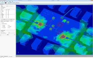 Figure 3. EM visualization
The design workflows for RFICs and mixed-signal ICs are very different from digital IC workflows, as outlined below.
Synthesis
Digital circuits consist of a small number of well-defined logic gates (like NAND). The circuit schematic is converted to a gate-level netlist expressed in a hardware description language like Verilog or very high-speed integrated circuit hardware description language (VHDL). During routing and placement, these gate-level constructs are then converted to on-wafer cells defined by the cell libraries in the selected fab’s process development kit (PDK).
In contrast, RF and mixed-signal ICs are analogue circuits with unique custom designs. The arrangements of resistors, inductors, capacitors, and active components into amplifiers, mixers, or other subsystems are often unique to each IC. They are not readily distillable into standard cells like digital gates are.
Instead, each subsystem is individually converted into on-wafer structures and interconnects. For example, an oscillator may utilise a complex configuration of transistors in feedback loops. The foundry PDKs for RFICs do provide process information, design rules, and models for active and passive components, but they are not as simple or standardised as digital ICs.
Simulation
In digital chip design, the digital nature of signals makes simulations relatively simpler. Digital IC simulations include various digital inputs and timing analyses.
In contrast, RFICs must contend with an infinite set of continuous high-frequency waveforms. Noise, parasitic effects, electromagnetic interference (EMI), and antenna effects emerge from the circuit arrangements as well as the physical on-wafer structures. So, realistic simulations are required at every step throughout the design cycle.
Verification
Design-rule checks (DRC) and implementation using a field-programmable gate array (FPGA) are common in digital IC design.
DRC verification tools are used in RFIC and mixed-signal semiconductor design as well. However, prototyping an RFIC with an FPGA is rare because its RF characteristics will be totally different. FPGAs are still used to verify the digital portions of mixed-signal ICs.
How do you choose the right EDA tool for a wireless electronic design project?
In addition to accurate RF and EM modelling and simulations, an essential feature is the ability to test the designs against wireless standards (like 5G and 802.11ad) right from the start.
This is possible using design tools that include virtual test benches (VTBs) for all the major wireless standards. VTBs ensure that the designs stay within the thresholds that standards place on signal power, noise, interference, and more.
What are the main challenges faced when using EDA tools in complex 3D circuit design?
Some of the main challenges in 3D RF circuit design include:
- modelling electromagnetic behaviours in 3D
- impedance matching
- noise
- linearity
- stability
- power consumption
- electromagnetic interference
- problems caused by increasing densification, like integrating different materials, 3D integration, and advanced packaging
What are the key features to look for in EDA tools for effective RFIC Design?
For effective design of RFICs and mixed-signal ICs, look for these key features:
- Advanced simulation algorithms developed for Keysight RF instrumentation and Keysight RF EDA software ensure equivalent results between virtual simulations and physical measurements.
- Fast-envelope techniques, compact test signals, and distortion EVM make simulation run times practical for RFIC designs in data-intensive, high-bandwidth mmWave or sub-THz applications, including 5G/6G, electric vehicles, and AI-enabled systems.
- Authentic waveforms and VTBs incorporate system context when simulating designs, enabling teams to optimise RFIC designs for their intended system applications sooner and successfully integrate first-pass into physical devices and systems.
Keysight RFIC EDA tools
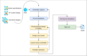 Figure 4. Keysight RFIC EDA tools
Keysight’s ecosystem of EDA tools streamlines RFIC and mixed-signal IC design, simulation, and verification. For large design teams looking for high productivity, the Keysight designcloud enables offloading RF and EM simulations to high-performance cloud platforms for rapid results and quick design cycles. The main design and simulation tools for RFICs and mixed-signal ICs are outlined below.
Keysight Advanced Design System (ADS)
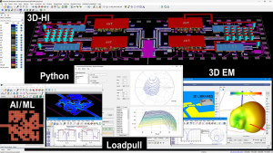 Figure 5. Keysight ADS
The Advanced Design System is tailored for high-frequency RFIC and mixed-signal IC design and simulation. It achieves 3D heterogeneous integration (3DHI) of RFICs, MMICs, packaging, PCBs, and antennas using multi-technology modules. Key features are listed below.
- Multi-technology integration: ADS enables comprehensive 3D integration of chips, packaging, interconnects, and boards, facilitating realistic simulations of assembled products.
- Superior simulation capabilities: The platform’s advanced circuit-level RF simulations and EVM optimisations for mixed-signal ICs produce predictions that are close to real-world measurements.
- Comprehensive component libraries: The platform offers vendor component libraries and PDKs that include symbols and layout footprints, as well as high-accuracy RF and microwave models.
- Standards compliance: ADS enables verification against wireless standards like 5G, automotive radar, and 802.11ad.
- Flexible automation: ADS supports Python scripting for automation and integration with external applications like artificial intelligence (AI) and machine learning (ML) to streamline design and verification workflows.
RFIC Design (RFPro Circuit)
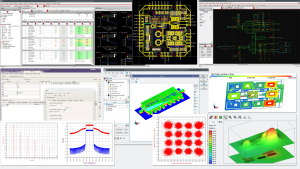 Figure 6. RFPro Circuit
RFPro Circuit is a specialised software for RFIC design. It can:
- model components on silicon chips accurately
- optimise designs with sweeps and load-pull analysis
- simulate RF designs in the Cadence Virtuoso and Synopsys Custom Compiler environments
- increase performance using Monte Carlo and yield analysis
- Assess error vector magnitude (EVM) for the latest communication standards early in the design phase
- Use the latest foundry technology immediately
Keysight RFPro
 Figure 7. RFPro
RFPro enables RFIC and MMIC designers to run interactive electromagnetic-circuit co-simulation for tuning and optimising their circuits. It includes 3D planar and full 3D finite element method EM simulators.
How are AI and ML algorithms integrated into Keysight RFIC EDA tools?
PathWave ADS provides Python application programming interface (API) endpoints for integrating AI frameworks like TensorFlow and PyTorch. This enables the use of advanced artificial neural network models in the design, modelling and simulation workflows.
How is Python integrated with Keysight EDA tools?
Keysight EDA tools provide Python API endpoints that expand custom features and improve usability.
For example, Python scripts can be used to control data analysis, simulators, and processes.
Python scripts enable the training of custom AI-based simulation models that are trained on measured or published data.
The post EDA Tools for Robust RFICs and Mixed-Signal ICs appeared first on ELE Times.
Newbie fixing newbie mistakes.
 | Hey everyone. Just wanted to kinda quickly introduce myself. My dad was always fixing radios, and was a generally great with electronics but he never thought about teaching me (probably because I was always more into art and music idk). Now I'm in my 40's and I decided to get into it, as a kind of connection to my late father, whom I really miss. Last Saturday I fixed my instrument and I bought a DYI tetris handheld and I will teach my son.. or rather we'll learn together. [link] [comments] |
India’s Vision for 6G: Use-Case Driven Innovation and AI-Enabled Networks
Courtesy: Jessy Cavazos, 6G Solutions Expert, Keysight Technology

As the world prepares for the next leap in wireless technology, India is shaping a bold and inclusive vision for 6G, one that goes beyond speed and latency to address real-world challenges. In a recent interview, Mohmedsaeed Mombasawala, Keysight’s General Manager for Industry Solutions in India, and a key contributor to 6G research efforts in India, shared insights into how the country is approaching 6G with a unique blend of pragmatism, innovation, and social impact.
A Use-Case First Philosophy
India’s 6G strategy is fundamentally use-case driven, a departure from traditional infrastructure-first rollouts. Rather than focusing solely on technical specifications or spectrum availability, the country is prioritising solutions that address societal needs, especially in sectors like agriculture, healthcare, and logistics.
This approach is particularly relevant for India’s vast and diverse population, where connectivity gaps persist in rural and remote areas. Mombasawala emphasised that 6G must be more than a technological upgrade: it must be a platform for transformation.
“We’re not just building networks. We’re building solutions for farmers, doctors, and supply chain operators,” he explained.
By anchoring 6G development in real-world applications, India aims to ensure that the technology delivers tangible benefits to communities that have historically been underserved by previous generations of wireless infrastructure.
AI-Native Networks: Intelligence at the Core
One of the most exciting aspects of India’s 6G vision is the emphasis on AI-native radio access networks (RAN). In this model, artificial intelligence isn’t just a tool; it’s a foundational design element. AI will be embedded throughout the network, enabling dynamic spectrum allocation, predictive maintenance, and real-time optimisation of resources.
This shift reflects India’s strength in software and data science, positioning the country to play a key role in intelligent network design. It also aligns with global trends toward more autonomous and adaptive systems, where networks can learn, evolve, and respond to changing conditions without human intervention.
“AI will be central to how we manage, scale, and secure 6G networks,” Mombasawala noted. “It’s not just about efficiency, it’s about enabling new capabilities.”
Spectrum Strategy: Balancing Reach and Performance
While many countries are exploring high-frequency bands for ultra-fast data rates, India is taking a pragmatic approach to spectrum. The focus is on frequency range 3 (FR3) bands, which offer a balance between performance and coverage. These midband frequencies are well-suited for India’s geographic and demographic diversity, allowing for a broader reach without the need for dense infrastructure.
This strategy reflects a deep understanding of India’s connectivity landscape, where rural access remains a critical challenge. By prioritising spectrum that supports ubiquitous coverage, India is ensuring that 6G can serve both urban innovation hubs and remote villages.
Collaborative R&D and Global Engagement
India’s 6G efforts are deeply collaborative, involving academia, startups, industry leaders, and government agencies. Mombasawala highlighted the importance of cross-sector partnerships in driving innovation and ensuring that 6G solutions are both technically robust and socially relevant.
At the same time, India is actively participating in global standardisation efforts, contributing to international dialogues while tailoring its approach to local needs. This dual strategy—global alignment with local customisation—is key to building a 6G ecosystem that is both interoperable and inclusive.
A Blueprint for Inclusive Innovation
India’s vision for 6G offers a compelling blueprint for countries seeking to balance technology innovation with social impact. By focusing on use cases, AI-native design, and inclusive spectrum planning, India is not just preparing for 6G; it’s redefining what 6G can be.
This approach challenges the notion that next-generation technology must be exclusive or elite. Instead, it positions 6G as a tool for empowerment, capable of transforming lives and industries across the socioeconomic spectrum.
“We want 6G to be a catalyst for change,” Mombasawala concluded. “Not just in how we connect, but in how we live, work, and grow.”
The post India’s Vision for 6G: Use-Case Driven Innovation and AI-Enabled Networks appeared first on ELE Times.
Introduction – hardware engineer from China, sharing a custom pulse signal generator
 | Hi everyone, [link] [comments] |
When Silicon Meets the Human Nervous System: A Deep Dive Into Neural Interfaces
Before examining the challenges and opportunities in bioelectronics, it is essential to understand how electronics and the human body converge. The human body—intrinsically organic and biological—can now interact with silicon-based systems through chips, interfaces, and digital extensions that do more than observe; they actively influence physiological function and enable measurable outcomes.
At its core, the human nervous system is among the most sophisticated electrical networks known. Every sensation, movement, and cognitive process originates as an electrical impulse transmitted across billions of neurons. Bioelectronics builds on this foundation by developing electronic systems capable of reading, interpreting, and modulating these neural signals with high precision.
At the centre of this convergence lies neural interface technology—where electronics, materials science, neuroscience, and computation intersect. What began as experimental neural signal recording has evolved into intelligent, closed-loop systems designed to interact with the nervous system in clinically and functionally meaningful ways.
The Nervous System: An Electrical Network
To call the human nervous system an electrical network is to acknowledge the fact that neurons communicate via action potentials—brief voltage changes produced by ionic movement across cell membranes. These electrical impulses propagate along nerve fibres and form the basis of basic human senses, including perception, motion, and cognition.
However, from an engineering standpoint, neural activity resembles a signal source but with certain riders. The biological signals that the neurons communicate through are characterized distinctly from conventional electronic systems in the following ways:
- Extremely low amplitude (microvolt range)
- Highly variable across individuals
- Sensitive to physiological and environmental conditions
- Embedded in a noisy, living medium
These complexities change the entire course of the environment and approach, which is a crucial aspect of the electronics system design, and that’s why bioelectronics is not simply applied electronics—it is fundamentally a new class of system design.
The Neural Interface Challenge
A neural interface is the physical and electrical bridge between living tissue and electronic systems. Basically, it is a technological innovation that enables a direct communication pathway between the brain (nervous system) and an external device, allowing thoughts/neural signals to control machines, and machines to send sensory data back to the brain. Its primary functions are twofold:
- Reading neural signals
- Delivering electrical stimulation
This makes the landscape more challenging, owing to the complex mix of an artificial arrangement to be balanced with a natural or organic system, and making it perform efficiently and adaptively. To this effect, the challenge lies at the interface level itself. Electronics are rigid and static; biological tissue is soft, adaptive, and reactive. Any long-term interface must balance electrical performance with biocompatibility.
Key Challenges in such an arrangement include:
- Mechanical mismatch between electrodes and tissue
- Immune responses that degrade signal quality
- Corrosion in ionic biological environments
- Stability over years, not months
Dr. Ben Rapoport, Co-founder and Chief Science Officer of Precision Neuroscience- the rival of Neuralink, notes that innovation is increasingly focused on minimising invasiveness: “That’s a big misconception, he said. People often incorrectly assume that ‘you need electrodes that penetrate deep inside the brain to get that information out.”
He further adds that Precision lies in developing a thin film that sits on the brain and records the brain activity. This reflects a broader industry trend toward surface-level and flexible neural interfaces rather than deep, rigid implants.
Neural Interfaces Making Gradual Emergence
Industry experts increasingly emphasise that neural interfaces are no longer speculative technologies. Yet these are gradually making space in our lives, making them more common in overall human behavior.
According to Kevin Hughes, Information Scientist of the Chemical Abstracts Service (CAS), which tracks emerging science and engineering domains, “With the recent news that Neuralink is approved to begin human trials, it’s clear that bioelectronics like brain-computer interfaces (BCIs) are moving out of the realm of science fiction and into reality.”
In the very same continuity, he also points out the difference that the industry is witnessing between the number of journals and the number of patents filed in the biotechnology landscape. The following graph shows the starkly lower number of commercial patents, while academic research has outpaced the same in the last 5 years. He writes, “his suggests that large-scale commercialization of these technologies faces fundamental scientific challenges that are being studied at the academic level and may be years away.”
Capturing Neural Signals: An Analog Problem
Neural signal acquisition is fundamentally constrained by analog design challenges. Electrical signals captured at neural electrodes typically exist in the microvolt range, making them highly susceptible to corruption from noise sources such as muscle activity, motion-induced artefacts, electrode impedance variability, and external electromagnetic interference. Unlike many conventional sensing environments, the biological interface itself is dynamic, lossy, and electrically unstable.
To this effect, the front-end electronics gets to play the most decisive role. These must provide:
- Ultra-low-noise amplification
- High input impedance
- Strong common-mode rejection
- Extremely low power operation
Unlike conventional sensors, neural interfaces cannot rely on static calibration. Signal properties drift over time due to biological adaptation and tissue response, demanding adaptive hardware and software co-design. Consequently, effective neural signal acquisition increasingly relies on adaptive architectures, where analog hardware, digital signal processing, and software algorithms are co-designed to track signal drift, compensate for variability, and maintain reliable performance over extended operational lifetimes.
From Signals to Interpretation
Raw neural signals carry no explicit meaning. Interpretation requires computational models capable of identifying patterns associated with intention, perception, or pathology. This has made way for Machine learning, hence making it central to modern bioelectronics. Models must continuously adapt as neural signals evolve, making on-device intelligence essential and timely.
According to BIOS Health, a company focused on AI-driven neural interfaces, this represents a new data modality in medicine:
“At BIOS, we’re developing AI-powered neural interfaces to allow us to read and write neural signals as a new data modality in healthcare… we can decode it, use biomarkers to see how a disease is progressing, and we can change those electrical signals. In doing so, we’ve delivered a therapeutic—we’ve treated a disease.”
This highlights a shift from monitoring systems to active bioelectronic therapies.
Writing to the Nervous System: Electrical Stimulation
Neural interfaces are not limited to passively observing neural activity; they are equally defined by their ability to actively influence the nervous system. This capability is most clearly demonstrated in modern bioelectronic devices that deliver precisely controlled electrical stimulation to targeted neural pathways. By injecting carefully shaped electrical pulses, these systems can alter neural firing patterns in ways that restore, suppress, or modulate biological function.
Electrical stimulation underpins a wide range of therapeutic and functional outcomes, including:
- Restoration of sensory input
- Modulation of dysfunctional neural circuits
- Enablement of motor control
- Suppression of chronic pain signals
From an engineering standpoint, effective neural stimulation demands precise control over parameters such as pulse amplitude, width, frequency, and waveform shape. These parameters must be tailored not only to the targeted neural population but also to long-term safety constraints, including charge balancing and tissue compatibility. Overstimulation risks tissue damage or neural fatigue, making precision and reliability non-negotiable design requirements.
Increasingly, neural stimulation systems are evolving into closed-loop architectures, where real-time sensing, on-device computation, and adaptive stimulation form a continuous feedback cycle. Instead of delivering fixed stimulation patterns, these systems dynamically adjust outputs based on measured neural responses, enabling more personalised, efficient, and clinically effective interventions. This shift from open-loop to closed-loop control represents a critical step toward truly intelligent bioelectronic systems.
Case Study: Cochlear Implants
Cochlear implants remain one of the most successful examples of bioelectronics in practice. Rather than amplifying sound acoustically, cochlear implants convert audio signals into electrical stimulation patterns delivered directly to the auditory nerve. Frequency components are mapped spatially along an electrode array implanted in the cochlea.
Despite delivering a simplified representation of sound, cochlear implants exploit the brain’s neural plasticity. Over time, users learn to interpret these electrical patterns as meaningful auditory experiences. From an engineering perspective, cochlear implants demonstrate:
- Long-term biocompatibility
- Ultra-low-power embedded processing
- Robust signal mapping
- Effective closed-loop adaptation
They validate the principle that bioelectronics succeeds when it works with biology rather than attempting to replicate it perfectly.
Power, Reliability, and Longevity
Implanted bioelectronic systems must operate reliably for years without failure. Power consumption, heat dissipation, and battery safety are critical constraints.
Unlike consumer electronics, failure carries direct clinical risk. As a result, bioelectronic design prioritises stability, redundancy, and conservative validation over rapid iteration.
Conclusion
The future of bioelectronics lies in deeper integration and softer interfaces—flexible electronics, bio-compatible materials, and adaptive systems that learn continuously. As silicon systems become more biologically aware, neural interfaces are evolving from experimental tools into foundational technologies for healthcare and human–machine interaction.
Bioelectronics does not aim to replace the nervous system. It aims to understand it—and, where possible, support it—using electronics designed to operate on biology’s terms.
The post When Silicon Meets the Human Nervous System: A Deep Dive Into Neural Interfaces appeared first on ELE Times.
[OC] CircuiTikZ Visual Editor - Build LaTeX circuits visually in your browser
![[OC] CircuiTikZ Visual Editor - Build LaTeX circuits visually in your browser](https://preview.redd.it/ff4mrezzkdbg1.png?width=640&crop=smart&auto=webp&s=51eca235a4597bcceed580e9f71eb6c86ac3b6a2 "[OC] CircuiTikZ Visual Editor - Build LaTeX circuits visually in your browser") | Hi everyone! I've just uploaded a project I've been working on to GitHub: CircuiTikZ Visual Editor. Link: https://github.com/mangel21/CircuiTikZ-Editor What it doesIt’s a web-based tool designed to make drawing circuits for LaTeX much faster. Instead of typing out coordinates, you can:
Please note that this is a very early version. It's still premature and there are many things to improve (more components, better wire routing, etc.). I am not a developer either, I'm just an electronics engineer who wants to build circuits faster. I would love for you to try it out and see if it helps your workflow. Also, please help improve it. If you are a developer, feel free to contribute or suggest features on GitHub! Let me know what you think! [link] [comments] |
Пам'яті Євгенія Володимировича Кривоногова

26 листопада 2025 року загинув випускник Навчально-наукового машинобудівного інституту 2018 року (кафедра лазерної техніки та фізико-технічних технологій, наразі в складі НН ІМЗ), старший лейтенант Євгеній Володимирович Кривоногов.
LoRaHunt - Monitoring live traps for invasive species
 | Invasive species pose a serious threat to native wildlife and ecosystems. LoRaHunt enables efficient monitoring of live traps, supporting responsible management and relocation efforts. Powered by an ESP32-based Heltec WiFi LoRa 32 (V3), the device primarily operates in deep sleep mode to maximize battery life, achieving up to three months of operation on four 18650 batteries. When a trap is triggered, a reed switch wakes the ESP32 to transmit the event and wait for acknowledgment. Twice-daily heartbeat signals confirm system status, eliminating the need for mandatory manual inspections. [link] [comments] |
Weekly discussion, complaint, and rant thread
Open to anything, including discussions, complaints, and rants.
Sub rules do not apply, so don't bother reporting incivility, off-topic, or spam.
Reddit-wide rules do apply.
To see the newest posts, sort the comments by "new" (instead of "best" or "top").
[link] [comments]
I can't believe this thing actually works
 | submitted by /u/ILike_Bread17 [link] [comments] |
Researchers shrink ferroelectric memory stacks

Researchers in Japan have developed ultrathin ferroelectric capacitors that maintain strong polarization at a stack thickness of just 30 nm, including top and bottom electrodes. Using scandium-doped aluminum nitride films sandwiched between platinum electrodes, the team achieved high remanent polarization, demonstrating the potential for high-density, energy-efficient memory in compact electronic devices.

The work, led by Professor Hiroshi Funakubo of Science Tokyo in collaboration with Canon ANELVA, marks a departure from previous approaches that only thinned the ferroelectric layer. By optimizing the full capacitor stack—5-nm platinum bottom electrode, 20-nm (Al0.9Sc0.1)N ferroelectric layer, and 5-nm platinum top electrode—the researchers maintained robust ferroelectric performance while drastically reducing device size.
Key to the success was a post-heat treatment of the bottom platinum electrode at 840°C, which improved its crystal orientation and enhanced polarization switching in the ultrathin films. This process ensures that the scaled-down capacitors remain compatible with semiconductor integration, enabling on-chip embedding alongside logic circuits.
The breakthrough lays the groundwork for compact ferroelectric memories, such as FeRAM and ferroelectric tunnel junctions, for future IoT and mobile electronics. By further exploring alternative electrode materials and processing techniques, the team aims to create even more durable, energy-efficient, and miniaturized on-chip memory devices.
Full details on the research are available here.
The post Researchers shrink ferroelectric memory stacks appeared first on EDN.
Inturai launches quantum-safe ESP32 security

Inturai Ventures, in partnership with cybersecurity firm PQStation, has unveiled quantum-safe encryption for connected devices across the defense, aged care, and home security sectors. Under the agreement, Inturai holds exclusive rights to deploy PQStation’s technology in these markets. The collaboration focused on securing MQTT traffic using post-quantum cryptography (PQC) on the ESP32 platform. Billions of devices worldwide run on the ESP32, a dual-core microcontroller SoC with integrated Wi-Fi and Bluetooth.
 Example ESP-32 device that can now run Post Quantum Secure. (CNW Group/Inturai Ventures Corp.)
The encryption was tested in two configurations: one using only post-quantum cryptography and another combining PQC with conventional security. Both approaches maintained strong performance, with low latency and minimal power impact, demonstrating that even small, low-power devices can operate securely against future quantum threats.
Governments across the United States, Canada, Australia, and the European Union are requiring post-quantum security upgrades to begin by 2026. In some jurisdictions, including Australia and the EU, critical sectors such as defense and healthcare must complete the transition as early as 2028.
This joint development with PQStation is central to Inturai’s mission to protect critical data in real-time sensor networks and positions the company to deploy quantum-safe protocols across critical sectors worldwide. Inturai expects significant benefits across its healthcare, drone, and military pipeline from this breakthrough, as the global ESP32 module market is projected to reach $4.6 billion by 2032 (Dataintelo).
The post Inturai launches quantum-safe ESP32 security appeared first on EDN.
OWC rolls out 2-meter Thunderbolt 5 cable

Other World Computing (OWC) offers a fully certified 2-meter Thunderbolt 5 (USB-C) cable for both Macs and PCs. Engineered with signal amplification, precision shielding, and end-to-end signal integrity, the cable delivers a long-length solution for workflows that require maximum speed, display performance, and power delivery—along with the full capabilities of Thunderbolt 5.

This extended-length cable joins the company’s lineup of 0.3-meter, 0.8-meter, and 1-meter Thunderbolt 5 cables. It is Thunderbolt-certified and validated by multiple independent testing labs to meet the complete Thunderbolt 5 specification, including:
- Up to 80-Gbps bidirectional data throughput
- Up to 120-Gbps video bandwidth for multi-display, high-performance workflows
- Up to 240-W power delivery
- Supports up to three 8K displays
- Fully compatible with Thunderbolt 5, 4, and 3, as well as USB4 and USB-C devices—universal for virtually any USB-C host or power/charging connection
The 2-meter Thunderbolt 5 cable costs $79.99 and is now available for pre-order, with delivery expected in early January 2026.
The post OWC rolls out 2-meter Thunderbolt 5 cable appeared first on EDN.
PicoScope 7.2 enables smarter waveform analysis

Pico Technology has released a major upgrade to its PicoScope software, improving waveform capture, analysis, and measurement. Version 7.2 adds built-in features like waveform overlays and advanced serial filtering, enabling faster, clearer, and more efficient control of PicoScope PC-based instruments.

Waveform Overlays is a visualization tool that displays multiple waveform captures stacked in a single view. This feature makes it easier to spot intermittent glitches, jitter, and anomalies often missed in single-shot captures.
New serial decoding filters make it easy to pinpoint specific packets, data types, or date ranges without combing through long serial captures. These advanced filters work seamlessly across all 40 serial protocols supported by PicoScope 7.
To learn more about what’s new in PicoScope 7.2, click here. It is available as a free update for all existing and new PicoScope users on Windows, Mac, and Linux operating systems.
The post PicoScope 7.2 enables smarter waveform analysis appeared first on EDN.
Compute modules are built for industrial AI

Based on Qualcomm’s Dragonwing IQ-X platform, Advantech’s three edge AI compute boards deliver up to 45 TOPS of AI acceleration for industrial applications. The AOM-6731 AI module, AIMB-293 mini-ITX motherboard, and SOM-6820 COM Express Type 6 module offer powerful processing alongside robust 5G and Wi-Fi 7 connectivity.

Leveraging Oryon CPUs with up to 12 cores running as fast as 3.4 GHz, Dragonwing IQ-X enables rapid data handling and seamless multitasking while consuming up to three times less power than competing solutions. Single- and multithreaded compute performance is further enhanced by on-device Hexagon NPUs, bolstering AI capabilities. Integrated Adreno VPUs and GPUs support multimedia-intensive applications.
Onboard LPDDR5x memory achieves a 1.3× speed boost—from 6,400 MT/s to 8,533 MT/s—while reducing power consumption by 20% versus standard LPDDR5. UFS 3.1 Gear 4 storage increases data transfer speeds from 1,000 Mbps (PCIe Gen3 NVMe) to 16,000 Mbps. UFS 4.0 is also available for optimal performance in harsh industrial environments.
Samples of the AOM-6731 AI module and SOM-6820 COM Express module are now available, while the AIMB-293 motherboard will be offered for engineering evaluations starting March 2026.
The post Compute modules are built for industrial AI appeared first on EDN.
An intimidating vacuum tube

Older table-top AC-DC radios used a classic line-up of tubes. Think 12SA7, 12SK7,12SQ7, 35Z5GT, and 50L6GT. As I grew into my teens, I got interested in how these radios worked and soon discovered that their vacuum tubes could get very hot, especially the last two, the half-wave rectifier (35Z5GT) and the beam power tetrode audio output stage (50L6GT).
One day, I carelessly allowed a window curtain to brush against a hot 50L6GT, and the fabric of that curtain actually melted. Mom was not thrilled.
With that history still fresh in mind, I later came across another vacuum tube called the 117L7/M7GT whose data sheet looked much like this:
 Figure 1 A datasheet for the 117L7/M7GT with the two hottest tube functions from previously studied radios in a single unit.
This thing was scary!
The two hottest tube functions from the radios I’d been studying were combined into one device. Both functions were placed within a single glass envelope vacuum tube.
Take a look at these guys:

Figure 2 Two 117L7/M7GT tubes combining the heat of the beam power tube and the rectifier tube within a single glass envelope.
Imagine the combined heat of the beam power tube and the rectifier tube within a single glass envelope. If the one tube that damaged Mom’s window curtain was thermally dangerous, I cringe to think how hot these tubes could get and what damage they might be capable of causing.
I still shudder at the thought.
John Dunn is an electronics consultant and a graduate of The Polytechnic Institute of Brooklyn (BSEE) and of New York University (MSEE).
Related Content
- Vacuum tubes are dead; long live vacuum tubes
- Unique vacuum tube benefits from additive manufacturing
- Vacuum tube technology resurrected
- The Mystery of the Vanishing Vacuum Tube
- Is There Still a Vacuum Tube in Your Future?
The post An intimidating vacuum tube appeared first on EDN.
Government’s Green Signal to 22 projects under ECMS
The Ministry of Electronics and IT has supposedly approved 22 new projects under the Electronics Components’ Manufacturing Scheme on January 02, 2026, with a projected investment of ₹41,863 crore and production of ₹2,58,152 crore.
The said proposals include those from Dixon, Samsung Display Noida Pvt Ltd, Foxconn (Yuzhan Technology India Pvt Ltd), and Hindalco Industries. These are expected to provide nearly 33,791 direct employment opportunities. This approval comes after the Ministry approved 24 proposals under the ECMS earlier.
The approval letters were handed directly by Union Minister Ashwini Vaishnav to those part of the above 22 projects on Friday.
As per a background note circulated by the Ministry on the third tranche of approvals, the nod includes the manufacturing of 11 target segment products that have cross-sectoral applications, such as mobile manufacturing, telecom, consumer electronics, strategic electronics, automotive, and IT hardware.
Of 11 products, 5 are bare components such as PCBs, Capacitors, Connectors, Enclosures, and Li-ion Cells; 3 pertain to sub-assemblies such as Camera Modules, Display Modules, and Optical Transceivers; and 3 are supply chain items such as Aluminium Extrusion, Anode Material, and Laminate.
The background note said the approvals aim to significantly strengthen domestic supply chains, reduce import dependence for critical electronic components, and support the growth of high-value manufacturing capabilities in India.
The post Government’s Green Signal to 22 projects under ECMS appeared first on ELE Times.
Beyond technology: ST’s commitment to educating and inspiring next generation
ST is well known as a global company creating technology and driving innovation. But it’s not just that. Its role extends beyond manufacturing products: the company is committed to inspiring and educating future generations by supporting scientific research, STEM initiatives, and engaging in talent development. This article provides an overview of ST’s recent and ongoing educational activities across key regions, including Italy, France, Singapore, and the United States.
Activities Across STEM, university relations and talent developmentST maintains a strong presence in the communities where it operates, participating in local and national events. Through various initiatives, the company connects with a broad spectrum of audiences, from primary and secondary school students and university graduates to experienced researchers. This commitment is further amplified through the ST Foundation, which leverages technology and education to drive social progress, promoting digital inclusion for disadvantaged communities globally. Regardless of the audience’s level of expertise, ST’s goal remains the same: promoting scientific culture and making the complex processes that lead to the production of our chips understandable.
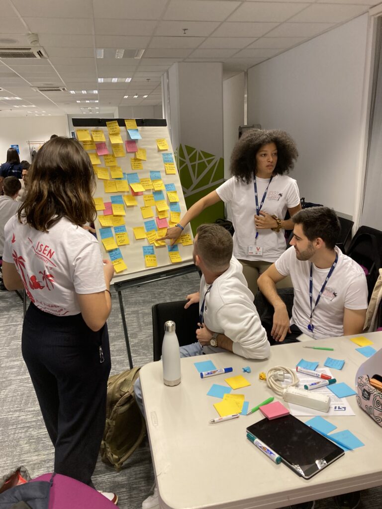
Recent educational events in ItalyIn Italy, ST organises more than 200 events annually, reaching approximately 18,000 students ranging from preschool to high school and university. Below are some of the key initiatives we’ve recently organised.
Neapolis Innovation Summer Campus Participants at Neapolis Innovation Summer Campus
Between late August and early September, the ST site in Arzano (Naples) hosted the twelfth edition of the Neapolis Innovation Summer Campus in collaboration with five universities in Campania. This annual ten-day training program is intended for bachelor’s and master’s degree students who want to explore the use of 32-bit microcontroller platforms and seek an opportunity to interact with industry experts. The initiative offered intensive, hands-on seminars at the ST site and provided a kit of components for the project work that students presented at the end of the event. Additionally, the event hosted small and medium enterprises and start-ups throughout its entire duration, allowing them to present themselves and build connections with young talent.
Researchers’ Night in MilanIn September 2025, ST took part in the Researchers’ Night in Milan, an event promoted by the European Commission as part of the Marie Skłodowska-Curie Actions, hosting research centres, institutions, universities, and organisations engaged in scientific dissemination. ST showcased its Edge AI technology: one of the demos included the LSM6DSV80X sensor with the STEVAL-MKI247A board, connected to the SensorTile.box PRO, and demonstrated how to monitor high-impact activities in soccer (for example, between the player’s shoe and the ball) and collect valuable information for game analysis.
Maker Faire Rome – European Edition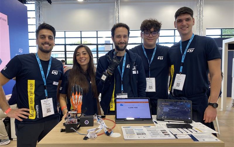 The STEM student winners of the 12th edition of the Neapolis Innovation Summer Campus 2025 with the smart glove “Hermes’ Hand”.
We also participated in Maker Faire Rome – European edition. This annual event has a varied audience, from school to university students, to startups, companies, and government institutions. Visitors could interact with demos in different fields, such as electronics, augmented reality, artificial intelligence, robotics, gaming, music and art. ST organised workshops covering Edge AI, robotics, and the STM32 Open Development Environment. A highlight was the “Hermes’ Hand”, a smart glove developed by a STEM student of the 12th edition of the Neapolis Innovation Summer Campus 2025. This project uses the STM32G474RE, X-NUCLEO-IKS4A1, and custom-made MEMS sensors to translate one’s voice into sign language in real time, breaking down communication barriers.
Science Festival in Genoa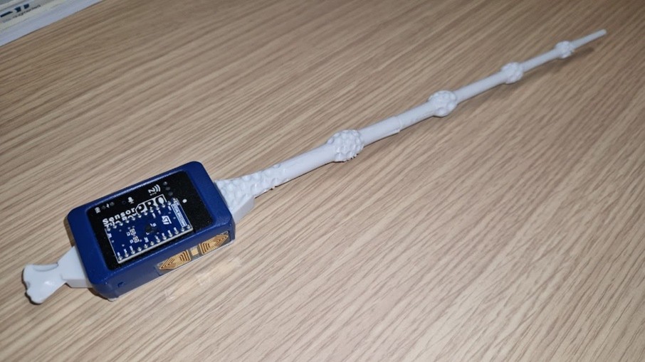 The “magic” wand demo
Another event held at the end of 2025 and aimed primarily at young students and families was the Science Festival in Genoa. ST presented “AI in your hands”: a magic wand, waved by visitors, demonstrated how the Integrated Signal Processing Unit (ISPU) in MEMS sensors can process movement locally (at the edge). Limited dependence on the cloud ensures high response speed, low power consumption, and greater security. Behind the playfulness and the visitors’ amazement, therefore, there was not magic but rather powerful local data processing.
Agreement with Polytechnic University of Turin
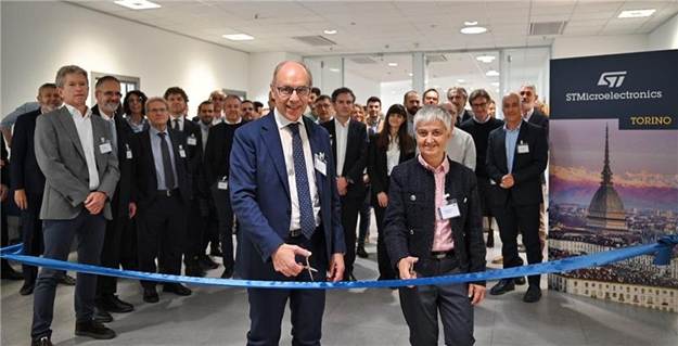 Inauguration of ST’s new design centre at the Polytechnic University of Turin. In the picture, Pro-Rector Elena Baralis and CEO of STMicroelectronics Italy Alberto Della Chiesa
To strengthen its ties with universities, in October, ST and the Polytechnic University of Turin renewed their framework agreement for the next four years and celebrated the inauguration of a new ST design centre space. The collaboration focuses on research and training of undergraduate and graduate students, particularly in fast-evolving fields such as cybersecurity, AI, and energy efficiency. Since 2019, STMicroelectronics has hired over 200 graduates (bachelor’s, master’s, and doctoral degrees) from the Polytechnic University of Turin. Many undergraduate and graduate students also work on their theses with the help of ST employees at the Turin centre.
Educational initiatives in FranceIn France, there is a virtuous example showing how recruitment needs in the field of microelectronics can favour high-level training for students and professionals. ST is one of the actors in the I-NOVMICRO program, a consortium of different companies that promotes microelectronics and electronics careers and provides advanced training in the Southern French Region (Rousset, Toulon, Sophia-Antipolis).
 Participants at I-NOVGAME
Launched in 2019, this initiative directly addresses recruitment needs by offering specialised training that qualifies people for technical sectors, particularly manufacturing jobs. Since the beginning of the project, more than 15,000 people have been trained, from secondary schools to baccalaureate level. This program allows students to learn semiconductor manufacturing processes in real-world conditions: facilities include an educational clean room and an educational grey room dedicated to maintenance training. The program also finances and leads a network of 12 Fab Labs in local high schools, coordinated by ST Rousset, and promotes STEM disciplines through school visits. The project’s ambition is to reach out all the whole of France and then expand on a European scale.
I-NOVMICRO also includes:
- I-NOVGAMES, an STM32 engineering and application challenge involving six engineering schools.
- INNOV ISLAND, a dynamic Metaverse offering a digital and 3D environment for training, educational materials, conferences, and job dating for students and employees.
Beyond direct training, ST supports education through donations of unused laboratory equipment, computers and STM32 microcontroller boards every year to schools and partners. Our company also offers career guidance through diverse programs and initiatives, primarily focused on engaging young people and supporting students with disabilities:
- For industrie, l’Univers Extraordinaire is a digital educational event which presents industry professions to young people through video game formats. ST participation includes virtual tours of ST facilities, video interviews with Rousset employees, and live presentations by industry professionals.
- Programs for students with disabilities at the Rousset site. Voyage au cœur de l’entreprise (VACLE) allows eight pupils to explore a dozen different professions over the course of a week, while Mentorat au coeur de l’entreprise (MACLE) is a mentorship program for high school students, where volunteer employees support students throughout their academic career, helping them plan their future, understand corporate culture, and develop their soft skills.
 On the left, participants at For industrie. On the right, a videogame screenshot.
Open-source and hands-on education with universities and partners in the US
On the left, participants at For industrie. On the right, a videogame screenshot.
Open-source and hands-on education with universities and partners in the US
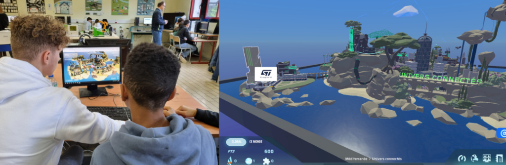
ST products and solutions can be useful for developing open-source programs. In the United States, for example, ST contributes to research and education by developing open-source curricula with a strong emphasis on hands-on learning. Professors at the universities we collaborate with (including MIT, UCLA, UC Berkeley, Rensselaer Polytechnic Institute, UC Santa Cruz, and Santa Clara University) use ST development tools, such as the popular STM32 microcontroller platform, in their courses, which are then publicly available on our website. One main area of development now is to adapt the existing curricula to the AI era, which is strongly affecting the job market and how students interact with hardware and firmware programming. For this reason, ST is working with organisations like the MIT CSAIL Alliances (Computer Science and Artificial Intelligence Laboratory) on research, particularly regarding AI computing on devices at the edge and applications in robotics.
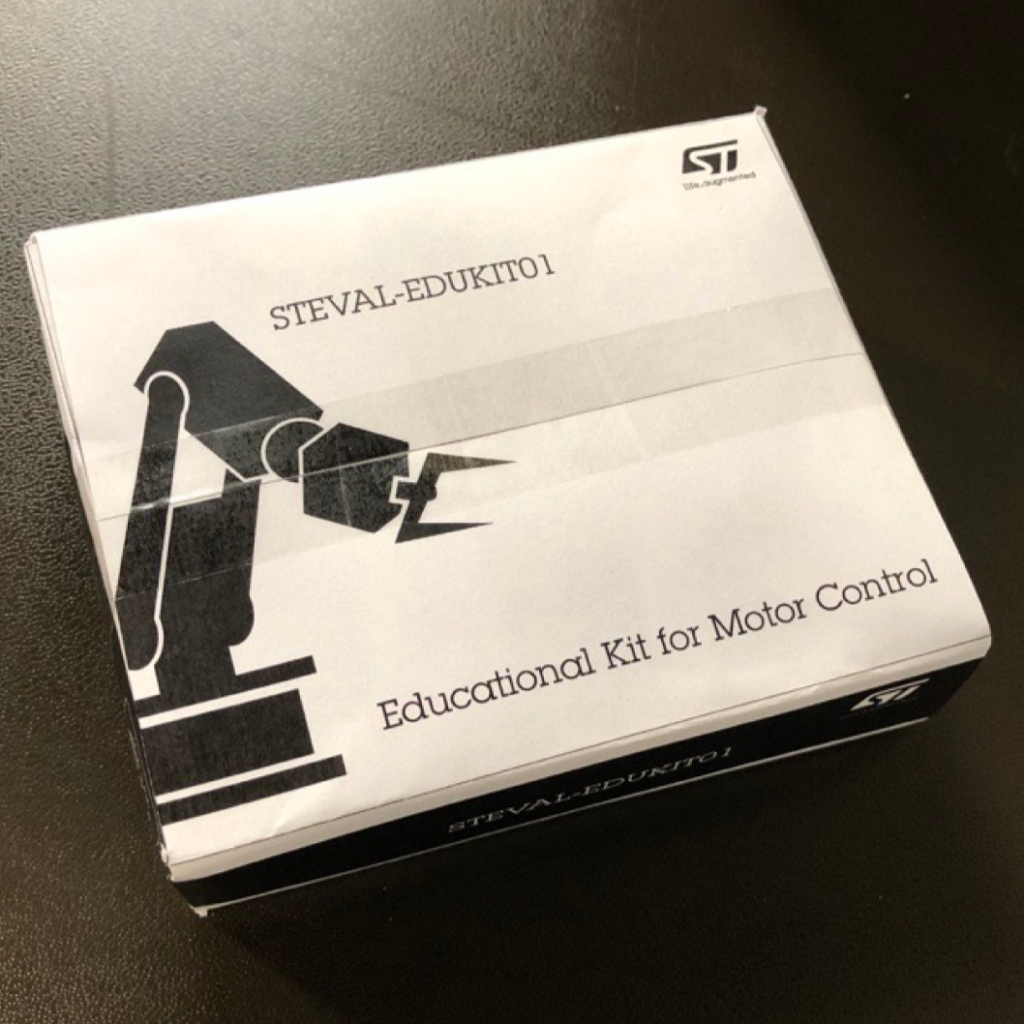 The STEVAL-EDUKIT01
Furthermore, we collaborate with partners who share our vision. With ARM, we have formed an Educational Alliance to support new curricula that will help students gain the necessary skills to become the professionals of the future. Some of these programs were developed in collaboration with the university and published on EdX, reaching over 40,000 enrollments over a four-year period. ST, SparkFun (member of ST Partner Program), DEKA and the Worcester Institute of Technology developed the Experiential Robotics Platform (XRP), an open-source platform for STEM education. Among other things, the XRP is the main provider of educational kits for the FIRST Robotics Competition, the largest STEM competition in the world, which targets primary and secondary schools and registered 785,000 participants in the 2024-25 school year.
Educational initiatives have helped ST products become among the most popular educational products in the United States. The STEVAL-EDUKIT01, developed in collaboration with UCLA, is the first ST development kit designed specifically for education and offers teaching materials for motor control and control systems.
Skills development and positive social impact in Singapore Participants at the STEM Fest organised by United Women Singapore
In Singapore, ST is adopting an educational approach that spans the entire learning journey, from primary schools to higher education. The goal is to drive a positive social impact and bridge the skills gap in semiconductor manufacturing by aligning education with industry needs. This comprehensive approach also focuses on inclusion addressing gender imbalance in the industry. To this end, ST partners with the United Women Singapore (UWS) to implement STEM initiatives for girls, such as the UWS STEM Fest. These initiatives provide mentorship, coaching, and networking to encourage more women to pursue STEM careers. Furthermore, ST fosters creativity and social responsibility in partnership with the Singapore Institute of Technology through the SIT Community Challenge. This program challenges students to develop sustainable technology solutions addressing real-world community issues such as urban mobility and environmental sustainability, directly supporting Singapore’s Smart Nation goals.
ST collaborates with Universities like the Singapore Institute of Technology (SIT) and the Institute of Technical Education (ITE). Our company develops and reviews curricula in microelectronics and semiconductor manufacturing through faculty exchange programs, ST guest lectures and participation in academic advisory committees to ensure relevance to industry demands. Additionally, ST provides practical experience through extensive vocational training, including the Integrated Work-Study Program (IWSP) in collaboration with SIT and Work-Study Diplomas (WSDip) offered by ITE, which provide students with up to 12 months and two years, respectively, of internship experience alongside ST professionals.
ST also invests in future talents through scholarships, including the Singapore Industry Scholarships (SgIS) and the Engineering and Tech Programme Scholarship (ETPS), which support students from pre-university through tertiary education. The flagship STICan (ST I Can) Work Experience Program (WEP) offers students aged 15 to 22 internships across the semiconductor value chain, from R&D and chip design to wafer fabrication and marketing. The program provides technical exposure and personal development courses to prepare students for university and careers.
ConclusionST’s engagement in educational and STEM activities serves a dual purpose: cultivating the next generation of talent while contributing to societal progress. From university partnerships to global outreach events, these initiatives form the foundation of ST’s commitment to driving innovation and developing technology responsibly for the future.
The post Beyond technology: ST’s commitment to educating and inspiring next generation appeared first on ELE Times.
Сторінки


![[link]](https://i.redd.it/djpnf0nbahbg1.jpeg)
![[link]](https://i.redd.it/ff4mrezzkdbg1.png)