


Збирач потоків
A comparison of traditional and DSP-enabled ADCs in radio receivers

In a radio receiver, the analog-to-digital converter (ADC) sampling rate and the complexity of the analog anti-alias filter in front of it are not independent choices. A sampled system can uniquely represent signals only over a bandwidth of Fs/2, so any content falling outside the chosen Nyquist zone must be removed before it reaches the converter. The closer the sampling rate sits to the theoretical minimum, the narrower the filter’s transition band becomes, and the higher the filter order required to reach a given attenuation.
Sampling faster relaxes that filter. The reason designers do not simply sample much faster is the cost on the other side: a higher sampling rate means a more expensive converter and more data for the downstream FPGA or ASIC to process. The optimum sits wherever those two costs balance, and in a conventional signal chain, it’s the digital side that limits how far the balance can move.
That constraint changes when the converter itself performs the processing. ADCs are now available that integrate a DSP block alongside the ADC cores, providing decimation, digital downconversion (DDC), and IQ mismatch correction on chip.
Because the decimator reduces the output data rate, sampling faster no longer adds to the downstream burden; in fact, it can reduce it. The optimum moves toward higher sampling rates with relaxed analog filtering, and a significant portion of the digital front-end moves off the FPGA at the same time.
This article works through three radio receiver designs: a direct conversion receiver, a direct conversion receiver with digital channel selection, and an IF sampling receiver. These are each built around a 14-bit dual-channel ADC with an embedded DSP block from Silanna’s SD1148 family, which offers sample rates from 40 to 250 MS/s.
- Direct conversion receiver
The direct conversion, or zero-IF, receiver architecture shown in Figure 1 uses a quadrature RF mixer that converts the RF signal directly to baseband. The signal chain starts with a band-select filter followed by a low noise amplifier (LNA), and the local oscillator (LO) is centered on the RF signal band.

Figure 1 Here is a simplified architecture of a direct conversion receiver. Source: Silanna
The mixer has two paths, one producing the in-phase (I) output and the other the quadrature (Q) output. So, a quadrature LO signal with sine and cosine components is required.
The baseband IQ signal path following the mixer typically consists of a programmable gain stage, an anti-alias filter, and finally the ADC. Many implementations include additional filtering along the signal chain and some amount of RF gain control. Channel selection can be either analog (by changing the LO frequency) or digital, in which case the LO frequency is fixed.
The entire band of interest is digitized by the ADC, and digital downconversion plus filtering are used to select the desired channel. Even with analog channel selection, channel-select filtering is often performed partially in the digital domain.
Implementation challenges
The direct conversion architecture does not have to deal with image rejection, as the signal is its own image. Its implementation challenges lie in LO feedthrough, 1/f noise, and gain transients. In the baseband, these issues are concentrated in the vicinity of DC and are most severe for systems using narrow channel widths, measured in kHz.
They are easier to deal with when using wider channel widths and modulations that are less sensitive to low-frequency content. When digital channel selection is used, placing the LO between channels largely solves them.
Another challenge is IQ mismatch: amplitude and phase mismatch between the I and Q components, which results in leakage between the I and Q signal paths. All baseband blocks, the mixer, and the LO contribute to this mismatch.
Differential gain errors between the I and Q paths in the mixer, amplifiers, and ADCs, together with the filter passband gain, contribute to gain mismatch. Phase mismatch is caused primarily by phase error between the LO sine and cosine components, by mismatch in the filter frequency response, and, to a lesser degree, by clock phase mismatch between the two ADCs.
Using dual devices for the amplifier and the ADC that are specifically designed for IQ applications significantly reduces the contribution from these blocks. Calibration is commonly required to suppress the remaining mismatch to a tolerable level. For signals with modest bandwidths, a frequency-independent calibration is typically sufficient.
Sampling rate and anti-alias filtering
ADC sampling-rate selection and baseband filtering are tightly coupled. Sampled systems, including ADCs, can uniquely represent signals only over a bandwidth of Fs/2, where Fs is the ADC sampling frequency. This condition is known as the Nyquist criterion.
If the ADC input contains spectral content in both the region from 0 to Fs/2 (the first Nyquist zone) and the region from Fs/2 to Fs (the second Nyquist zone), the sampling process folds frequency components from these regions onto one another. This effect is called aliasing and must be avoided. Either region can be used to place the signal of interest, but not both simultaneously.
The anti-alias filter is an analog filter placed in front of the ADC to suppress unwanted signal and noise content outside the selected Nyquist zone prior to sampling. When the signal band extends to Fs/2 − Δf, the frequencies that must be fully rejected by the filter begin at Fs/2 + Δf, giving a transition band 2Δf wide.
The narrower the transition band, the higher the filter order required to achieve a given attenuation. For this reason, it’s advantageous to increase the ADC sampling rate beyond the theoretical minimum stated by the Nyquist criterion in order to relax the filter specification. This margin is typically at least 30% and is often higher.
The trade-off is higher ADC cost and increased digital signal-processing requirements versus the cost and complexity of analog filtering. An ADC with an embedded DSP block offsets the digital processing burden, which shifts the optimum toward higher sampling rates with relaxed analog filtering.
Design example
The first example uses the dual ADC in a direct conversion receiver. The RF signal is a 26 MHz-wide band centered at 915 MHz. After downconversion, the baseband I and Q signals extend from 0 to 13 MHz. The ADC sampling rate is set to 65 MS/s, which provides a relaxed anti-alias filter transition band from 13 MHz to 52 MHz.

Figure 2 The above configuration represents a direct conversion receiver application. Source: Silanna
As shown in Figure 2, the DSP block offers adders and multipliers that can be programmed to correct the DC offset and the IQ gain mismatch. Hardware for IQ phase correction is also present. The user provides the control values for these blocks.
The DSP block includes a decimator that can be programmed for rates of two and four; in this case the rate is set to two. The decimation process includes a digital finite impulse response (FIR) low-pass filter whose passband is 40% of the output sampling rate, which here is 0.4 × 65 MHz/2 = 13 MHz, matching the requirement.
When a low-pass filter is applied to the I and Q paths separately, the combined effect produces a symmetric band-pass response centered at 0 Hz, resulting in a passband from −13 MHz to +13 MHz. Figure 3 shows the frequency-domain signals at each step of this direct conversion receive chain.

Figure 3 Here is how frequency domain signals look like in a direct conversion receiver. Source: Silanna
The decimator has reduced the output sampling rate to 32.5 MS/s. The combination of oversampling and digital filtering improves the signal-to-noise ratio by about 3 dB for every decimation factor of two.
One consequence is worth noting. Because the decimation filter suppresses signals in its stop band, it can affect the gain control loop of the system. If a strong signal is present at the ADC input, but is filtered out of the digital output, a loop that monitors the output might not detect that the ADC is starting to clip. This can be avoided by incorporating the overrange bit provided by the ADC into the gain control algorithm.
- Direct conversion receiver with digital channel selection
The second example operates on the same 26 MHz RF band, now divided into four 6.5-MHz channels. The application receives one channel at a time, occasionally switching between channels.


Figure 4 The radio receiver design uses a built-in DDC to perform channel selection within the digitized band. Source: Silanna
The RF and analog portion of the receiver remains the same as in the first example. We enable the digital downconverter built into the ADC, shown in Figure 4, and tune the numerically controlled oscillator (NCO), which provides the digital LO to the center frequency of the desired channel. This shifts the selected channel to 0 Hz, as shown in Figure 5. The decimation factor can then be programmed to four, reducing the output sampling rate to 16.25 MS/s.


Figure 5 Frequency domain signals are shown in a direct conversion receiver using digital channel selection within the digitized band. Source: Silanna
We can also consider reducing the ADC sampling rate from 65 MS/s to the 50–55 MS/s range, which maintains reasonable anti-alias filter requirements while further reducing the output data rate. Using these DSP blocks offloads a significant amount of digital signal processing from the FPGA to the ADC, providing both cost and power savings.
- IF sampling receiver
The third example uses an IF sampling radio architecture, which is essentially a superheterodyne receiver in which the second downconversion stage is implemented digitally. A simplified block diagram is shown in Figure 6. The RF signal is converted to baseband in two steps: first to an IF, where it is digitized, and then to baseband using a digital mixer.

Figure 6 IF sampling receiver converts RF signal to baseband in two steps. Source: Silanna
This architecture eliminates the IQ matching issues and the challenges in the vicinity of DC associated with direct conversion receivers. The improvement comes at a cost: the system must achieve image rejection, which typically requires more analog filtering.
In addition, the ADC input is at a higher frequency, which demands a higher-performance ADC and places tighter requirements on sampling-clock jitter. A common way to keep the ADC sampling rate reasonable is to locate the input signal in the second (or third) Nyquist zone. In the IF sampling receiver, the ADC input signal is real, requiring only a single ADC per receive chain instead of a dual-channel device.

Figure 7 IF sampling receiver is show with DSP’s DDC and decimation functions enabled. Source: Silanna
In this example, we process a 40 MHz RF signal in the 2.4 GHz ISM band. This requires an increased sampling rate than in previous examples, and the 210-MHz device from the same family was selected. The IF is chosen as 150 MHz, which places the image 300 MHz away from the desired signal at RF.
The ADC sampling rate is chosen as 200 MS/s, which centers the IF in the second Nyquist zone. Operating in higher Nyquist zones requires band-pass anti-alias filtering; in this case the lower stopband is from DC to 70 MHz, the passband is from 130 MHz to 170 MHz, and the upper stopband is from 230 MHz and above.

Figure 8 See the frequency domain signals in IF sampling receiver. Source: Silanna
The aliasing effect, which in this case is a useful feature of the sampling process, is used to bring the signal to a 50 MHz center frequency. It’s worth noting that a signal sampled from the second Nyquist zone appears spectrally inverted, so the alias that lands in the first Nyquist zone is flipped relative to the original. Figure 8 shows the spectrum of the signal throughout the signal chain.
Negative frequencies are typically omitted when dealing with real signals, as they are a mirror image of the positive frequencies. Here, however, it’s useful to note that the signal image in the negative frequencies is not flipped relative to the original analog signal. With this insight, we can enable the DDC and program the digital LO to −50 MHz. This rotates the spectrum by 50 MHz toward the positive frequencies, bringing the band to a 0-Hz center frequency with the proper orientation.
The image originally in the positive frequencies is now shifted toward Fs/2 and partially appears in the negative frequencies around −Fs/2. To remove this unwanted image and reduce excess bandwidth, the decimator must be enabled with a decimation factor of two or more. The 40-MHz signal bandwidth permits additional decimation, so the decimator is set to decimate-by-four.
This reduces the output sampling rate to 50 MS/s. Because we have translated a real signal into a complex one, we now have both I and Q components, which together carry the same data rate as a real 100 MS/s signal. The 40% decimator filter bandwidth results in a passband from −20 MHz to +20 MHz, a good fit for the 40-MHz signal band.
Common pattern in three RF architectures
The same pattern holds across all three architectures: moving decimation, digital downconversion, and IQ correction into the converter relaxes the analog filtering in front of it while reducing, rather than increasing, the data rate behind it.
In the direct conversion example, raising the sampling rate from 40 MS/s to 65 MS/s widened the anti-alias transition band by 2.8×, added 2.1 dB of oversampling gain, and still lowered the output data rate by 19%. In the channel-selection example, the output rate fell to 16.25 MS/s and the channel filter moved off the FPGA entirely. In the IF sampling example, a real 200-MS/s input became a complex 50 MS/s output with the unwanted image removed on chip.
The practical consequence is that the sampling-rate-versus-filter-order trade-off no longer must be settled in the analog domain alone. Where the digital front-end processing is effectively free, because it happens inside the converter, the optimum moves toward faster sampling and simpler analog filters, and a meaningful portion of the FPGA workload moves with it.
Mikko Waltari is director of data converter designs at Silanna.
Related Content
- Radio Architectures: ADCs and Receivers
- RF-sampling ADCs for multiband receivers
- A checklist for designing RF-sampling receivers
- Analyzing ADC Noise Impacts on Wireless System Performance
- ADC Parameters for Your Wideband Telecommunications Receiver
The post A comparison of traditional and DSP-enabled ADCs in radio receivers appeared first on EDN.
Mouser will stop selling and representing ADI
 | I was asking Mouser costumer support because I could not find some ADI chips in stock in their webpage and after some emails, they answered me with the image attached. English translation: "As for ADI's distribution, we will no longer be distributors; it's not that certain ADI products will be restricted, but rather that we will no longer represent them." So this confirms what has been talked several times about online sellers suddenly requiring identification for ADI purchases and stopping the B2C sells. --- For the mods: I know this is not a component level circuit question, but perhaps the topic is important enough to be posted. -- The black bars are there to hide personal names. [link] [comments] |
Fun with third-order active filters

Butterworth response circuits come in both low- and high-pass versions, as well as ideal, Sallen-Key, emitter follower and DC accurate variants.
Many decades ago, I published a Design Idea about using equal value resistors and capacitors to implement a third-order active filter with the classic Butterworth response. This topology required two or three unity gain op-amps, depending on where the first-order RC section was located. And by swapping the positions of the resistors and capacitors, you could switch from a low-pass to a high-pass Butterworth response, while the 3 dB corner response remains the same at 1/(2*pi*R*C).
Wow the engineering world with your unique design: Design Ideas Submission Guide
The normalized Butterworth polynomial of S^3 + 2*S^2 + 2*S +1 can be factored into (S + 1)*( S^2 + S + 1), thereby revealing a multiplied first-order and second-order quadratic. In the original filter, the first-order section could be placed either ahead of or behind the second-order section, with the later yielding a two op-amp version; the op-amps are unity gain and provide isolation between the sections. These are the Type I versions.
A while back, I began working with different active filter topologies, including a revisit of the original Sallen-Key Type I version with an emitter follower implementation used much earlier in a car radar application. In the process, I discovered another filter version, where the factored Butterworth polynomial is directly implemented with a single op-amp. This approach, which also works with equal-value resistors and capacitors as well as an op-amp configured with a gain of 2, is called a Sallen-Key Type II. This particular configuration has a pass band gain of 2, while the Type I has a gain of 1.
The emitter follower version was implemented by replacing the unity gain op-amps in the Sallen-Key Type I with an emitter follower, and can use either two or three emitter followers similar to the op-amp version Type I. With both versions, the emitter followers can be complementary (NPN and PNP, or visa versa) which achieves a better effective input-to-output DC offset voltage, since the VBEs cancel. Since the emitter follower has a voltage gain of slightly less than unity, this characteristic causes the amplitude response to fall between Butterworth and Bessel regions, although the phase response follows the classic Butterworth.
While continuing my investigation of various active filters, another topology popped up that apparently dates way back to early 70s Fluke DMMs (digital multimeters). Known as the DC accurate second-order low-pass filter, it was utilized as a voltage reference noise filter. This filter is quite interesting in that the filtering is achieved by shunt capacitors working against an input series resistance; the active op-amp has no resistive connection to the input or output and therefore contributes no offset voltage or bias current.
It’s also interesting (to me, at least!) that if the op-amp 2*R resistor feedback resistance is implemented with two separate series resistors of value R, along with a shunt capacitor to ground installed between them, this configuration transforms into a third-order Butterworth low-pass filter with equal-value resistors and capacitors. If the shunt capacitor to ground is then removed, the filter reverts back to a second-order Butterworth, albeit with a lower corner frequency by a factor of 2/pi. I found it quite amazing that removing a shunt capacitor to ground actually lowers the corner frequency of a low-pass filter!
Figure 1 shows the various forms of these low-pass filters for simulations, including an ideal filter version with the Butterworth transfer function.

Figure 1 The various third-order active Butterworth response low-pass filters discussed in this Design Idea include ideal, Sallen-Key Type I and II, emitter follower and DC accurate variants.
Figure 2 shows LTspice AC simulation results, illustrating the limitations of the op-amp output impedance on the stop-band rejection. Note that the emitter follower version has slightly less than unity gain and a slight deviation from the ideal response, as expected.

Figure 2 In these LTspice linear AC low-pass filter simulations, note the stop band attenuation limits due to op-amp model finite output impedance.
Figures 3a and 3b show actual lab measurements performed with a DSO (digital storage oscilloscope)/AWG (arbitrary waveform generator) combination, utilizing the built-in Bode feature, for various low-pass filters. Compare them with the previous simulations shown in Figure 2, and note the stop band limitations due to the finite op-amp output impedance.
 |
 |
Figure 3 Low-pass filter Bode measurements in the lab show stop band effects due to physical op-amp output impedance limitations (a, left). In the emitter follower version’s Bode plot, note that the DC gain is -0.6 dBV (b, right).
So far so good; this is getting increasingly fun for me as I move through these various active filter topologies, and hopefully you agree! The detailed analysis for each of these filter topologies, left as an exercise for the reader, is an interesting adventure that helps illustrate what’s going on. For now, there’s more exploration to come!
Now, lets swap the resistors and capacitors in each filter topology, thereby transforming each filter from a low-pass to a high-pass version (Figure 4). The only filter to complete this transformation with any negative effects whatsoever is the DC accurate version. With this particular filter, the DC isolation due to the shunt capacitors is now replaced with shunt resistors, which obviously couple the op-amp input and output offset to the filter output. Otherwise, this filter, like its peers, behaves as expected in its high-pass form.

Figure 4 Swapping resistors and capacitors results in high-pass versions of the circuits previously seen in Figure 1.
Figure 5 illustrates the simulation results with the resistor and capacitor swaps made to each previous filter type, thereby transforming it from a low-pass to a high-pass filter with the same characteristic (i.e., Butterworth) and 3dB corner of 1/(2*pi*R*C).

Figure 5 Shown here are simulations of the high-pass filter derivations of Figure 1’s circuits, i.e., the circuits shown in Figure 4, in each case achieved by swapping resistors (R) and capacitors (C).
Figure 6a and 6b are actual lab measurements which reveal some of the measurement setup and equipment limitations in dynamic range at the low-frequency end.
 |
 |
Figure 6 In these lab-based Bode high-pass filter measurements (again, a at left, b at right), note the dynamic range limitations at lower frequencies.
I hope that the Bode Plot lab measurements on actual hardware for both the various low-pass and high-pass filters, for comparisons with the simulation results, are helpful for you. The circuit were built using 1% tolerance resistors and 10% tolerance film capacitors, on plug-in protoboards. You can judge for yourselves as to whether the lab measurements and simulations are in reasonable agreement; reader thoughts on this topic or anything else regarding this Design Idea are welcomed in the comments. More generally, have fun with these active filters!
Michael A Wyatt is a life member with the IEEE and has continued to enjoy electronics ever since his childhood. Mike has a long career spanning Honeywell, Northrop Grumman, Insyte/ITT/Ex-elis/Harris, ViaSat and retiring (semi) with Wyatt Labs. During his career he accumulated 32 US Patents and in the past published a few EDN articles including Best Idea of the Year in 1989.
Related Content
- Dual amplifier active filters
- Toward better behaved Sallen-Key low pass filters
- Component tolerance sensitivities of single op-amp filter sections
The post Fun with third-order active filters appeared first on EDN.
GaN Power transistors: What 700 V and 100 V PowerGaN Bring to Power-Supply Design
Power designs now face the same demands at the same time: higher efficiency, smaller size, lower cost, and more power from the same space. For years, silicon has supported these designs. However, in a growing number of applications, it is close to its practical limits, and further optimisation increases losses and heat.
For this reason, gallium nitride (GaN) power transistors are receiving significant attention. ST has added a new 700 V and 100 V PowerGaN family to its portfolio and brings these advantages to mainstream power conversion. This article explains what the technology offers power designs and why it matters now.
Why Use GaN Power TransistorsGallium nitride is a wide-bandgap semiconductor and, in a power converter, its main advantage is speed. Gallium nitride (GaN) power transistors, also called gallium nitride high electron mobility transistors (GaN HEMTs), switch much faster than silicon devices and lose less energy each time they turn on and off. Two effects follow from this behaviour. Less energy is wasted as heat, and the converter can operate at a higher switching frequency without losses increasing as they do with silicon.
Almost every benefit of GaN results from these two effects. Until recently, the technology appeared mainly in specialised, high-end products where the cost was justified. With a broad 700 V to 100 V family now in production, GaN has become a practical choice for everyday power conversion across a wide range of designs.
Improved EfficiencyThe clearest benefit is efficiency. Because GaN has low conduction and switching losses, more of the input power reaches the load, and less of the power turns into heat. In ST reference designs, PowerGaN has achieved power-supply efficiency of up to 98.6%. Higher efficiency affects the entire design: lower operating costs, less energy consumption over the product life cycle, and lower demand on the cooling system.
For equipment that operates continuously, such as power supplies, lighting, and energy systems, even a small efficiency gain accumulates over thousands of operating hours. Efficiency is usually the first reason that a design team considers GaN, and it leads directly to the next two benefits.
Increased Power DensityThe second benefit is size. A higher switching frequency allows the bulky magnetic components and filters in a converter to shrink, and the rest of the design shrinks with them. That creates two options for a design team: deliver the same power in a smaller, lighter product, or fit more power into an existing enclosure.
Gallium nitride (GaN)-based designs have reached an average size reduction of around 50%, compared with earlier silicon equivalents, at power densities above 100 watts per cubic inch. For products with tight space and weight constraints, such as compact adapters, chargers, and on-board systems, that extra headroom can determine whether a design fits at all. Increased power density is where the move to GaN becomes visible in the finished product.
Reduced System CostThe third pillar is lower system cost. It results as much from the design around the transistor as from the device itself. A gallium nitride (GaN)-based converter uses smaller passive components and fewer passive components and often requires little or no heat sink. As a result, the overall system cost decreases, and the design is simpler.
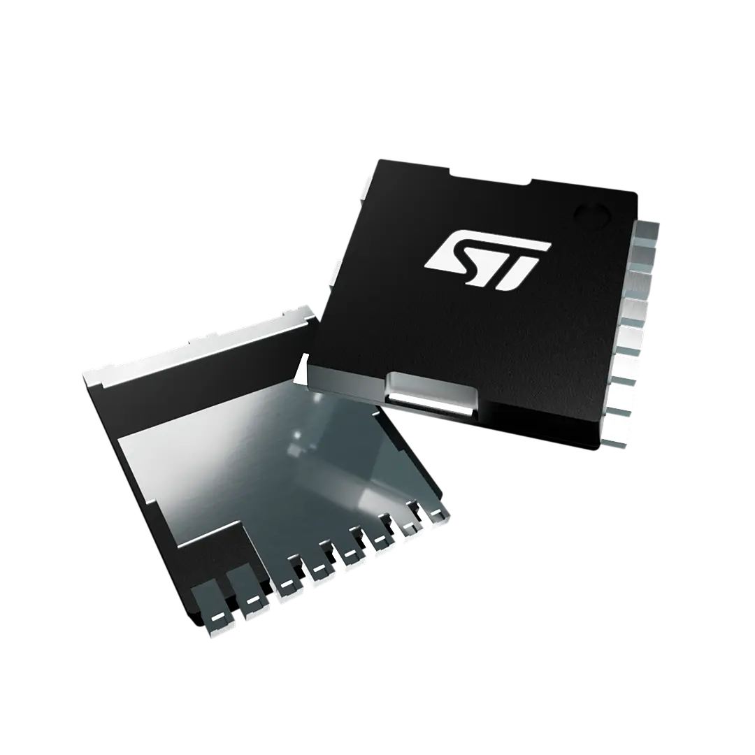
Cooler operation also improves reliability and life cycle, which means that the system tends to last longer and requires less servicing. Lower energy consumption over the product life cycle adds to the savings. Together, these effects reduce the cost of building and operating the system, and they are a large part of why GaN deserves its place in a design.
Where 700 V & 100V PowerGaN FitsThese benefits are not tied to a single product type. The same value higher efficiency, greater density, and lower total cost) extends across a broad range of designs, including AC-DC and DC-DC power supplies, USB Type-C adapters and chargers, LED lighting, motor control, AI servers, robotics, industrial systems, and advanced consumer applications such as home appliances, as well as power and energy systems such as solar and storage. The same value also supports the growing power demands of computing and electrification.
Across these areas, priorities differ, but the same three advantages apply. A choice of package options allows a design team to match the device to the power level and board layout of each application. Because the 700 V & 100V PowerGaN family is already in production and available, these benefits can already be built into designs today.
Backed by a Broad PortfolioAdopting a new switching technology is a decision about support as much as about the device itself. Alongside the 700 V and 100 V family, ST brings decades of power semiconductor experience, a broad product portfolio, a reliable supply chain, and strong technical support. For a team that works with GaN for the first time, that combination reduces the risk of the transition and shortens the path from an idea to a working design. It is part of what makes the value of PowerGaN practical rather than theoretical.
Why GaN, And Why NowGaN power transistors provide higher efficiency, greater power density, and lower system cost for power conversion. The new 700 V and 100 V PowerGaN family makes these benefits available to mainstream designs. For a design team that is considering the move to GaN, the technology has reached the point at which its advantages are practical today rather than promised for tomorrow.
The post GaN Power transistors: What 700 V and 100 V PowerGaN Bring to Power-Supply Design appeared first on ELE Times.
Q2 smartphone production down just 8% year-on-year, to 275 million units
From Silicon to Scale: Aheesa Signs Packaging MoU with Optilink Networks
Aheesa Digital Innovations, a DLI-scheme backed fabless semiconductor company headquartered in Chennai, has signed a Memorandum of Understanding (MoU) with Optilink Networks Pvt. Ltd., onboarding the company as its packaging partner for VIHAAN-I, Aheesa’s indigenous RISC-V broadband networking System-on-Chip (SoC). The partnership marks another step towards commercialising VIHAAN-I, strengthening the pathway from indigenous chip design and silicon validation to packaging, distribution and market deployment.
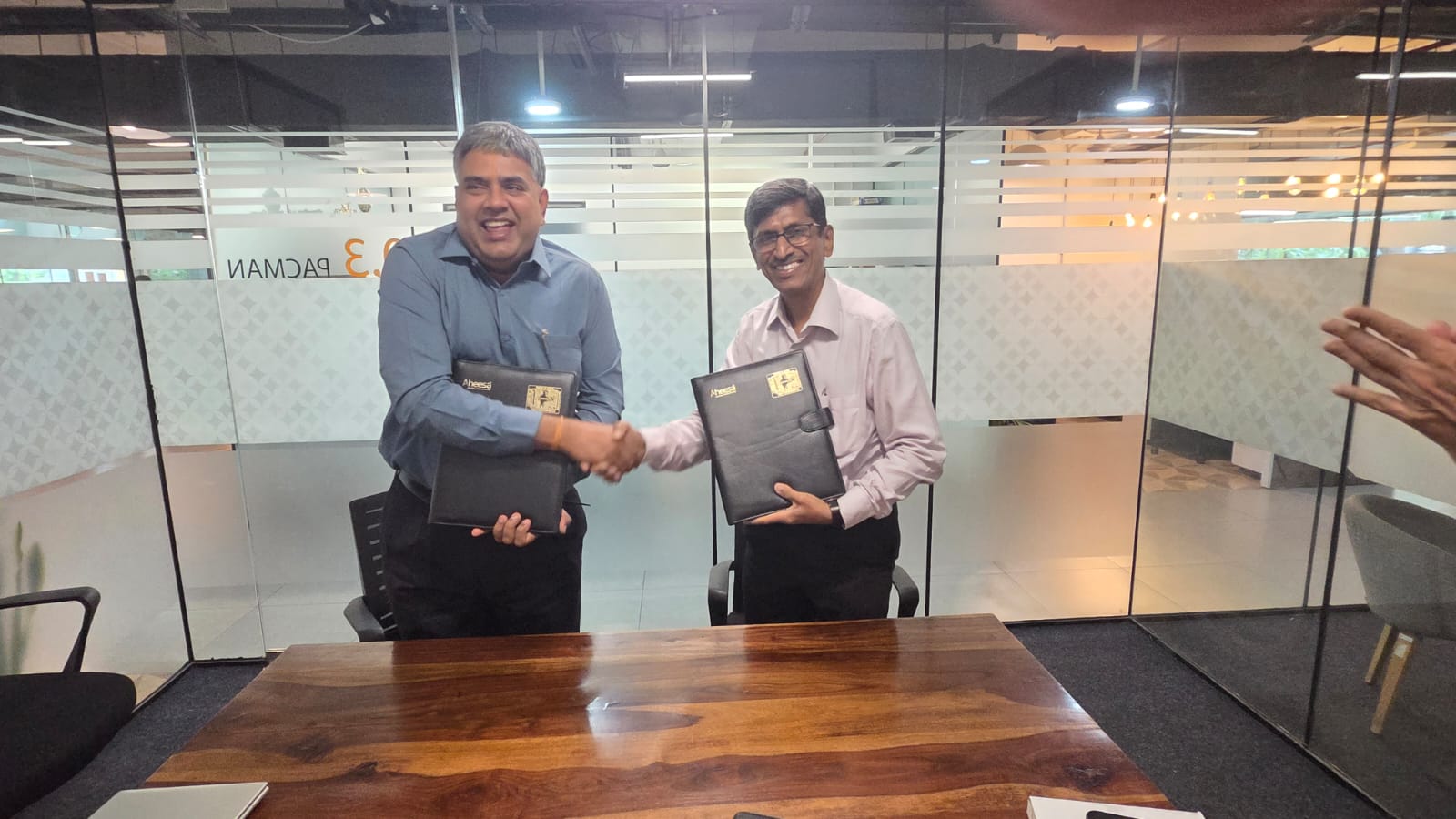
The partnership brings together two complementary parts of the broadband technology ecosystem. Optilink has supported the VIHAAN-I journey through testing, validation and engineering support, with its in-house capabilities across product design, firmware development and hardware integration. Under the MoU, Optilink will support end-to-end product development from prototyping to packaging, while the companies work towards developing, qualifying and commercialising ONT/CPE products based on the VIHAAN-I chipset. The collaboration is aimed at delivering solutions that are cost-efficient and comply with Indian and global standards, while accelerating commercialisation through Optilink’s engineering and manufacturing expertise.
This further advances Aheesa’s ambition to establish itself as a semiconductor design house with a portfolio of Indian-designed chips serving both domestic and global markets. With design, silicon validation, packaging and distribution capabilities progressively coming together, Aheesa is now leaping towards commercial deployment in early 2027.
The partnership comes in a landmark year for Aheesa. VIHAAN-I achieved tape-out on Republic Day 2026, followed by Aheesa securing investment from the Tamil Nadu Infrastructure Fund Management Corporation (TNIFMC) through the Tamil Nadu Emerging Sector Seed Fund. On this Independence Day, the chip achieved first-pass silicon success on its very first attempt.
Commenting on the partnership, Sridharan Mani, Founder and CEO, Aheesa Digital Innovations, said, “Building a chip is only half the journey as the real test is turning that silicon into a product people can use. No semiconductor ecosystem thrives on the strength of one player alone; it takes multiple partners, each doing their part, to carry a design to the consumer and make this sector succeed. With Optilink joining us for packaging, VIHAAN-I takes a step closer to that reality. We have spent years estabilishing that world-class semiconductor design can happen in India. Now with Optilink, we’re building the pathway to take it from systems to scale.”
Devchand Haria, Managing Director, Optilink Networks Pvt. Ltd said, “At Optilink, we’ve spent close to two decades building the networking hardware that connects Indian homes from fiber access to broadband CPE. Partnering with Aheesa for VIHAAN-I lets us bring that same experience to an Indian-designed chip, taking it from silicon to the products that will actually sit in Indian households. This is exactly the kind of collaboration our sector needs, that is Indian design and Indian manufacturing expertise working together to put homegrown silicon inside the devices people use every day.”
Founded in 2005 and headquartered in Mumbai, Optilink Networks Pvt. Ltd. is an Indian Original Equipment Manufacturer (OEM) that designs, manufactures and distributes IP-based networking hardware, Fiber-to-the-Home (FTTH) solutions and IP Television (IPTV) technologies. Serving ISPs, telecom operators, cable and MSO networks, enterprises and government customers, Optilink has built a strong B2B presence through its channel partners, distributors and system integrators across India.
Aheesa’s work spans indigenous semiconductor and networking technologies across telecom, broadband, cybersecurity and edge computing. This partnership now reflects the wider momentum in India’s semiconductor design ecosystem, now scaling under Semicon 2.0 — the ₹1,27,500 crore programme approved in July 2026 to build a globally competitive supply chain across chip design, manufacturing, packaging and materials. As indigenous designs move from validation towards commercial adoption, it is partnerships like this, pairing Indian chip design with the reach to deploy it, that will help define how homegrown silicon scales.
The post From Silicon to Scale: Aheesa Signs Packaging MoU with Optilink Networks appeared first on ELE Times.
Infineon Sets New Power Benchmark for AI accelerators and Vertical Power Delivery with 2 A/mm² Dual-Phase Smart Power Stages
Infineon Technologies AG introduces the TDA235E5 and TDA235E0, a dual-phase smart power stage family designed to meet the rapidly growing power density requirements of next-generation AI accelerators and vertical power delivery modules. Integrating Infineon’s OptiMOS 6 MOSFETs and a dual-phase driver IC in a compact 6 x 6 x 0.8 mm³ package, the new family delivers benchmark power density exceeding 2 A/mm², setting a new reference point for power stage performance in high current AI processor applications. As hyperscalers and datacenter operators continue to scale AI infrastructure, the demand for power delivery solutions that combine higher current capability with shrinking physical footprints is becoming a critical bottleneck.
“Infineon customers are designing AI systems that will define the next decade of computing infrastructure,” said Rakesh Renganathan, Vice President Power ICs at Infineon. “The TDA235E5 and TDA235E0 power stages give designers the power density, thermal performance, and design flexibility to move faster and build with confidence, backed by Infineon’s full AI server power delivery ecosystem.”
The two devices support up to 300 A peak current and 120 A total design current (TDC), making them well suited for next generation AI xPU accelerators as well as conventional server CPUs in datacenter environments. Both lateral and vertical power delivery configurations are supported, providing the design flexibility required as the industry transitions toward vertical power module architectures in advanced AI processor packages. Superior thermal impedance from junction to top side enables efficient liquid cooling integration, a characteristic that is increasingly important as power levels per processor socket continue to rise and traditional air-cooled thermal budgets are exhausted. Combined with Infineon’s digital multiphase controllers, the power stages support flexible, scalable multi-rail architectures that reduce time to deployment in fast-evolving AI server platforms.
The TDA235E5 and TDA235E0 integrate into Infineon’s end-to-end AI server power delivery ecosystem, spanning the full power chain from grid interface to processor core rails. By combining the complementary strengths of silicon, silicon carbide, and gallium nitride, Infineon provides datacenter customers with a proven, scalable path to the highest efficiency, robustness, and power density available for AI-optimized infrastructure. The datacenter power delivery market is one of the semiconductor industry’s fastest-growing demand segments, driving Infineon’s continued product investment to serve this opportunity at the component level where power density requirements are most critical.
The post Infineon Sets New Power Benchmark for AI accelerators and Vertical Power Delivery with 2 A/mm² Dual-Phase Smart Power Stages appeared first on ELE Times.
AWG
 | Hello everyone, Six months ago I set upon the journey of making my own AWG, with frequencies of up to 1MHz. 6 months later I present you my very own awg. I set out to build my own function generator after finding commercial units both too expensive and more general-purpose than I needed, and it looked like a good excuse to work through analog synthesis, filtering, and mixed-signal PCB design end to end. The sine path is an 8-bit R-2R ladder driven by a Raspberry Pi Pico W (overclocked to 225MHz) generating samples via a DDS phase accumulator; the square wave comes from the same chip’s PIO hardware. I started off with a breadboard and tried sallen key filters for noise but they amplified the noise aswell. I also tried discrete components for the sauare wave before replacing it outright with a TC4427 gate driver. The sine chain settled on a 5th-order doubly-terminated LC Butterworth reconstruction filter, replacing an earlier cascaded-RC design that was capping amplitude, followed by LM318 gain and buffer stages. Three PCBs went out; two came back dead. V1.0 was completely non-functional because a BOM matcher substituted 2.21Ω resistors for 2.21kΩ across the entire R-2R ladder. V1.1 moved to an all-SMD board with the LC Butterworth filter but came up dead silent; testing the square path first (it worked) narrowed the fault to the sine chain, which traced to a KiCad-to-Altium migration that had silently shorted two LM318 input pins onto one net. V1.2 fixed that short, soldered the Pico directly to the board in place of a socket, and came up working: sine characterised from 0Hz to 1MHz and square to 2MHz, with AM, FM, and noise modes added on top in firmware, all controllable from a Python desktop UI over USB. Looking at it now, a redesign with some improvements (better op-amps and also fewer) would be better but I also want to work on other stuff, so for now this is it. To be clear, I made every schematic and protoype and thought up everything myself. As such this may not be the best way to do this. My main goal, was experience after all. [link] [comments] |
As AI models scale 100x every two years, Yole maps shift from compute to communication
Заслужений професор КПІ Юрій Лукач. До 100-річчя від дня народження

Національний технічний університет України "Київський політехнічний інститут імені Ігоря Сікорського" відомий у країні і світі багатьма науковими школами, серед яких помітне місце займають започатковані на факультеті хімічного машинобудування (з 1999 року інженерно-хімічний факультет, а з 2025 – факультет автоматизації, промислової інженерії та екології) перші у країні школи процесів та апаратів хімічних виробництв, а також процесів та обладнання перероблення полімерних матеріалів. Неоціненний внесок у становлення й розвиток цих двох наукових шкіл зробив учасник Другої світової війни, доктор технічних наук, заслужений професор нашого університету, професор кафедри машин та апаратів хімічних і нафтопереробних виробництв, завідувач цієї кафедри впродовж 1973-1999 років Юрій Юхимович Лукач.
EEVblog 1770 - Rigol RSA800 Real Time Spectrum Analyser TEARDOWN + Reverse Engineering
Openai Astra really can do electronics design now
 | Here is my project repo https://github.com/fredriknk/chatgpt_astra_test2 I saw the Chatgpt Astra kicad demo, and wanted to try it out myself and im pretty damn impressed...! I only have a openai 20$/mo plus subscription so i had to use the lowest setting, but i got this design in 3 hours with 5 prompts in total and ate up my 3 usage resets. My only contributions to the design was to create the empty kicad template project, and the initial prompt: "Lets test a esp32 design with a 24v input voltage which can output and read 4-20ma signals. Lets start planning!"All design choices, component choices, design, schematics and, layout and documentation was done by the chatgpt astra 6 low through codex cli. So final verdict? Its actually pretty damn usable.... Like, its not perfect by any means. some examples: There are a quite a few routing decisions i dont agree with, especially the USB routing and unneccesarry internal layer routing. The schematics are very hard to read as it doesnt use GND/Power symbols, and only use global labels instead of wires. But as far as i can tell from the schematic, this is a working design and i do agree with a lot of its component choices. I feel it is pretty much where AI coding was in around 2024 (on its lowest setting), so im wondering where this will be in a year or two..! [link] [comments] |
Occam’s Razor and a USB-C to HDMI adapter

The simplest explanation is likely the best, even if its validity isn’t always intuitively obvious in advance.
Speaking of USB-C, and the cables (including splitters) that connect to it to other things…
My long-in-the-tooth Intel-based 2018 Apple Mac mini is still sitting on my desk, humming to my right, even though its M2 Pro Apple Silicon-based successor has been sitting downstairs in storage awaiting its turn in the spotlight for going on three years now. The legacy hardware is no longer a candidate for new Apple operating system releases, but it’s still receiving bug fixes and security patches, until sometime in the second half of next year, if past-history trends remain valid. And as the saying goes, “if it works, don’t touch it” (I’d also be tempted to haul out the “a penny saved is a penny earned” quote, but since I’ve already bought its replacement…).


In conjunction with my transition to it from its 2014-era Mac mini predecessor roughly 2.5 years ago, I upgraded the two-display suite above it to a set of Dell P2415Q 4K LCDs.

The Mac mini leverages the displays’ HDMI inputs; a “Project Volterra” Windows-on-Arm dev kit 2023 stacked above it connects to those same LCDs over their DisplayPort connections, and front panel buttons toggle the displays between the two systems when running concurrently.

Look back at that 2018 Mac mini rear panel “stock” photo a couple of paragraphs ago, however, and you’ll only see one HDMI output, into which I’ve plugged a “straight” HDMI cable running directly to one of the LCDs. How, then, did I connect the system to the other display’s HDMI input? That’s where today’s teardown victim enters the picture.
It’s an Anker A8730 6’ USB-C to HDMI adapter cable; I’d bought and pressed it into immediate service way back in mid-2021. I sourced from Anker’s outlet store on eBay, where it cost $25.90 as a refurb. So, you can say I’ve gotten my money’s worth out of it! Speaking of fiscal topics, there’s a 0.75′′ (19.1 mm) diameter U.S. penny alongside in the second (and non-stock) image that follows, along with subsequent others, for size comparison purposes.


How it works is (at least to me) an interesting story in and of itself. It fundamentally leverages a DisplayPort technology called “Alt Mode”, which repurposes USB 3.x’s “SuperSpeed” data and Configuration Channel (CC) lines to transport dedicated audio and video streams sourced from the graphics and sound subsystems. The CC leverage explains why, among other implementation reasons, it’s only applicable to USB-C, not also to prior-generation USB physical connector standards.
Macs don’t additionally support DisplayPort’s Multi-stream Transport (MST) mode, either in the operating system (generally) or in hardware (for newer Apple Silicon-based systems). If MST support had existed, it would have conceivable enabled me to extended-mode tether both displays to a single USB-C (or Thunderbolt 3, aka TB3, in this case) system connector, in combination with a separate inter-display connection. But again, per the system back panel photo, I had plenty of spare connector candidates available, not even counting those on the separate expansion hubs (the latter added subsequent to the snap of the earlier “stack” picture).


But what’s with all this DisplayPort talk? I thought we were discussing connecting the computer to a display’s HDMI input! We are, and that’s where the bulge surrounding the adapter cable’s HDMI connector end comes in. Conceptually, and I hope to definitively confirm today, inside is likely a DisplayPort to HDMI protocol-converting bidirectional transceiver; a particularly robust one, it seems, since the Anker A8730 touts 4K 60 Hz specs. HDMI once also had an “Alt” mode for USB-C, at least on specification paper, although actual products never made it to market.
Erratic function = dissection rationalizationSince the adapter cable had been operational in my abode since mid-2021 (and, considering it was a refurb, maybe even earlier than that with its original owner), why’d I decide to take it apart? Curiosity was as always one motivation, although I generally hold that particular urge at bay for as long as the gear remains operational. But this one had eventually failed, in another story-in-and-of-itself, through whose telling I aspire to also rationalize the “Occam’s Razor” title reference.
As previously mentioned, the 2018 Mac mini is still receiving periodic patches for its last-supported MacOS 15 “Sequoia” operating system release. A few updates ago, the left-side display of the pair (the one leveraging the Anker adapter) was no longer recognized by the system after the upgrade and subsequent reboot. Online research revealed that mine wasn’t a unique post-update quirk, and swapping the adapter cable to a different TB3 system connector got the display going again.
So, I figured that an obscure “Alt Mode” bug (specifically, since the first TB3 port still worked fine for generic data) introduced along with the upgrade had made it through Apple’s pre-release QA checks. This purported scenario was unsurprising albeit still disappointing, given that Intel-based Macs in general, and this system in particular, were on their “last legs” and likely no longer receiving their fair share of QA attention. Why my surmised bug only affected one TB3 port but not another wasn’t clear, but…
The next time I did an update, however, the exact same thing happened, this time to the second TB3 connector. Swapping the cable adapter back to the first TB3 connector didn’t resurrect the display. And I no longer had any other spare TB3 ports on the system available to try. At this point, I began to fear I had a fundamental system hardware degradation issue on my hands.
But after unplugging the cable adapter from the Mac mini and trying it with the “Project Volterra” system instead, where it also didn’t work, I was reassured by the now-nonfunctional repetition across multiple systems (and O/Ss) that a dead cable adapter was the likely culprit. An “Amazon Basics” cable adapter replacement fired up fine, sealing the Anker A8730’s fate.
What was behind the cable adapter’s initial failure, temporary resurrection, and eventual permanent demise? I hoped the pending teardown might provide visual Achilles’ Heel evidence (hold that thought). But I suspect it has something to do with MacOS’s use of display-supplied Extended Display Identification Data (EDID) information for software interface purposes versus Windows’ leverage of (when available) display-specific drivers.
My guess is that EDID (re-) enumeration in MacOS happens both when a display is first-time plugged into a new system connector and after each sufficiently impactful operating system update. In this particular case, the aforementioned DisplayPort HDMI bidirectional protocol translator in-between the system and display initially began operating erratically and eventually failed completely. But that’s just my conjecture; reader theories in the comments are as-always also welcomed!
Speaking of tearing down, let’s dispense with further abstract chit-chat and get to dissecting, shall we? Here are a few more real-life device photos as prep. Packaging is long gone at this point, along with any potential originally accompanying literature. The USB-C end, to start.

With a product-code sticker behind it.

Intermediary cable markings next.


And now the bulge-augmented HDMI other end, starting with the seam-less cable-intro side.

The connector side conversely does have a visible seam at its circumference.

But attempts to surmount it with hair dryers and heat guns, along with spungers and such, were for naught. So, I escalated my attack by breaking out the hacksaw with hopeful deft technique.


That’s what I’m talking about!


For anyone following in my footsteps who prefers a less Neanderthal-reminiscent dissection approach, here’s the HDMI connector-surrounding piece I was unsuccessfully trying to extract earlier. Note specifically the locations of the retention tabs.

Finally, what you’re all most interested in, the PCB. As I’ve mentioned before, “top”, “bottom” and other orientation terms are particularly nebulous where HDMI is concerned. So instead, here’s the side corresponding to the wider HDMI connector edge.

Now zooming in for a closer look.

I was admittedly surprised to encounter a preponderance of passives, given that the most common adapter-usage orientation would have put this side on top, with the remaining (and proportionally higher heat-generating) stuff you’ll see next on the other side and below it. Given that heat rises (don’cha know), and that there’s no passive ventilation venting available, that’s a seeming premature failure-inducing decision. But not in my case, since the HDMI connector points downward with this display, not horizontally straight out the back as with many others.

Components of particular note include a five-lead SOT23-packaged step-down (buck) DC-DC converter at lower left, marked as follows.
JWA5J
91D5T
There’s also a “2R2” (2.2 µH) inductor to its immediate left, and a 27 MHz oscillator to its right. And what does that clock chip likely drive? Let’s flip the PCB over to the other side.

Now that’s more like it (unless you’re into passives, that is). Again, we zoom in for a closer look.

At lower left is Via Labs’ VL100, a (surprise, surprise…not…) DisplayPort USB-C Alt-mode controller. To its right is (surprise, surprise…truly, this time, at least a bit…) another oscillator, 24 MHz this time. Continuing to the right is, I’m guessing (readers?), a serial interface nonvolatile memory for code and data storage purposes, marked as follows.
125S40
BG17K8
P19030
In the lower right corner is another JWA5J DC/DC converter. Above it is (once again, no surprise) Paradise Technologies’ PS176 DisplayPort to HDMI video interface converter. And again for the passives fans among you, there are plenty more examples to see on this side of the PCB, too!
That’s a “wrap” for today, folks. Share your thoughts with me and your fellow readers in the comments, please!
—Brian Dipert is the associate editor, as well as a contributing editor, at EDN.
Related Content
- USB-C’s lingering incompatibilities and other complexities, part 1: Direct-connect complications
- USB-C’s lingering incompatibilities and complexities, part 2: Splitter issues
- The 2025 WWDC: From Intel, Apple’s Nearly Free, and the New Interfaces Are…More Shiny?
- Connecting systems to displays with DVI, HDMI, DisplayPort: What we got here is failure to communicate
- USB: Deciphering the signaling, connector, and power delivery differences
The post Occam’s Razor and a USB-C to HDMI adapter appeared first on EDN.
Synopsys, COEP Tech University and CADFEM Establish Digital Twin and Multiphysics Lab in Pune
Synopsys, COEP Technological University and CADFEM India have setup the “Ansys Digital Twin & Multiphysics Lab” on the COEP campus, Pune to support advanced engineering education, research, and strengthen the industry-academia partnerships. This program holds huge significance in an ecosystem for automotive and electrical vehicle industry which utilizes the technologies for vehicle system’s product development and validation processes.
The laboratory was established as a part of Memorandum of Understanding (MoU) signed during the 2026 Symposium. It will provide students, researchers, and faculty members access to Ansys digital-twin technologies and advanced high-end multiphysics simulation tool that have been acquired by Synopsis. The lab will host industry training and certification, technical seminars and research.
Multiphysics simulation has a potential role in analysis of different physics domains in development process of the vehicle or component within EV industry. Engineers are able to investigate on battery thermals, electric motor efficiencies, power electronics functionality, structural strength, electromagnetic phenomenon and thermal management by simulation work-flows prior build physical prototype. Digital-twin methodology can create bridge between physics-based models and actual data taken from sensors and operation data so to monitor and predict system behaviours.
The post Synopsys, COEP Tech University and CADFEM Establish Digital Twin and Multiphysics Lab in Pune appeared first on ELE Times.
«Драйвова осінь» 2026

⛺️ У сквері "Сосновий" КПІ ім. Ігоря Сікорського відбувся традиційний фестиваль «Драйвова осінь» від туристичного клубу КПІ «Глобус».
India’s EV Component Industry Faces Technology Capability Gap as Imports Rise
India’s rapidly growing EV industry faces a capability gap in developing and producing high-technology components that can meet modern technology demands because about 80% of component manufacturers are small businesses built for traditional mechanical parts rather than advanced electronics and software. The capability gap involves areas such as batteries, power electronics, embedded software, advanced electronics, and system integration.
India is shifting more towards electric vehicles as its automotive supply chain expands. Original Equipment Manufacturer (OEM) sourcing of auto-components is expected to increase by 16% to 6.6 lakh crore by FY26 against components’ exports valued at around 2.1 lakh crore. However, import charges rise at a greater rate, with China covering about 36% of all the auto component imports India uses.
The capability challenge is particularly significant for small and medium-scale enterprises (MSMEs), which constitute almost 80% of Indian auto-parts producers. Though electronics, embedded software, advanced engineering, and system integration are key factors for competitiveness, a lesser than half the small and medium scale enterprises lack the capabilities required to develop and manufacture components as per the modern industry demands. Embedded software capability is estimated to be found in only 10% of domestic suppliers, whereas system integration, and product-development capabilities are around 14%.
The post India’s EV Component Industry Faces Technology Capability Gap as Imports Rise appeared first on ELE Times.
Indian Electronics Makers Turn to Aluminium as Rising Copper Costs Squeeze Margins
There is growing demand from Indian electronics manufacturers for alternatives to expensive copper such as aluminium, and a more widespread adoption of other cheaper materials due to increased cost pressure and lower profit margins as copper prices rocket. Companies are also encouraged to boost domestic procurement and re-engineer product and component designs to reduce dependence on these raw materials.
Copper is widely used across the electronics industry because of its electrical conductivity, robustness, and reliability. Due to recent surge in copper prices has increased manufacturing costs, creating challenges for companies especially those already facing a competitive market that might not be able to fully pass the rising input costs to consumers.
A recent report stated that the copper price has risen by around 45%, thereby decreasing manufacturers’ profit. Because of this, some Indian electronics manufacturers are now considering aluminium as an alternative to copper in applications whether it’s electrical, mechanical, and thermal properties are highly required to meet product specifications. Aluminium is being considered as a substitute of copper because it is lighter and cheaper.
The product design needs modification when using aluminium as a substitute to achieve performance comparable to that of copper. Using aluminium as a substitute for copper is not easy to practically implemented across all electronics applications. It is important for manufacturers to consider properties like electrical conductivity, thermal performance, resistance to corrosion, joining techniques, and product lifespan before adopting alternate materials.
The post Indian Electronics Makers Turn to Aluminium as Rising Copper Costs Squeeze Margins appeared first on ELE Times.
Pi-Ener-lite: Compact UPS with Fuel Gauge and RTC for Raspberry Pi Zero
Automotive Electronics Could Account for 50–55% of Car Cost by 2030, Enhancing Localisation Opportunities
Electronics will make up 50% to 55% of a car’s total manufacturing cost by 2030, growing significantly from 30% to 35% in 2020, creating a growth opportunity for Indian automotive component manufacturers in high-value electronic systems, according to a recent report by the Boston Consulting Group (BCG) and the Automotive Component Manufacturers Association of India (ACMA).
As per the report, increasing adoption of ADAS, infotainment, connected vehicle technologies, sensors, and ECUs in both ICE and EV vehicles are driving higher content of electronics.
However, India’s electrical and electronics segment was expected to be around 12% of domestic component supply in FY2025, highlighting significant scope for localization. Indian suppliers could capture a share of this emerging value pool, while also developing new capabilities in automotive electronics and other associated technologies.
Some technologies such as sensors, Electronic Control Units (ECUs), power electronics, connectivity systems, and Battery Management Systems (BMS) are gaining more consumer attraction as cars evolve into software-defined and highly connected products.
To capture this localisation opportunity, Indian component manufacturers need to move beyond traditional mechanical and manufacturing capabilities. They need to invest more in engineering, research and development, electronics design, software, testing, and technology development to compete in advanced technology that can be easily adopted by consumer mature automotive supply chains.
The post Automotive Electronics Could Account for 50–55% of Car Cost by 2030, Enhancing Localisation Opportunities appeared first on ELE Times.
India Approves Industry Production of DRDO-Developed Missile Systems
The defence minister, Rajnath Singh, has authorized the transfer of technologies, including conventional missile systems developed by DRDO, to eligible Indian defence manufacturers to set up indigenous production. In this process, mature and proven missile technologies are being moved from development to industrial-level mass production. The manufacturers will need to have applicable technical qualifications, certification levels, and regulatory requirements in place.
The scope for wider participation in the missile production chain would occur to some extent also due to technology transfer, where state-owned manufacturers, private firms, MSMEs & specialized manufacturers could develop expertise and participate in components and sub-components, electronics, propellants, guidance systems and associated mechanisms, launch systems and integration with greater depth.
There is scope for increased industrial involvement, which could bring about a higher level of domestic production and value addition, thereby lowering defence imports reliance. Increased industrial involvement could enable DRDO labs to focus more on research in newer and advanced technologies, while existing and developed systems may be produced industrially. A drastic policy shift, as it marks a change in treating private Indian companies as long-term technology and production partners in defence manufacturing. Its success hinges on technological absorption capability, quality testing procedures, test facilities, and orders.
The post India Approves Industry Production of DRDO-Developed Missile Systems appeared first on ELE Times.
Сторінки




![[link]](https://i.redd.it/w8u7wjxupaoh1.png)