
Збирач потоків
Silicon MOS quantum dot spin qubits: Roads to upscaling

Using quantum states for processing information has the potential to swiftly address complex problems that are beyond the reach of classical computers. Over the past decades, tremendous progress has been made in developing the critical building blocks of the underlying quantum computing technology.
In its quest to develop useful quantum computers, the quantum community focuses on two basic pillars: developing ‘better’ qubits and enabling ‘more’ qubits. Both need to be simultaneously addressed to obtain useful quantum computing technology.
The main metrics for quantifying ‘better’ qubits are their long coherence time—reflecting their ability to store quantum information for a sufficient period, as a quantum memory—and the high qubit control fidelity, which is linked to the ‘errors’ in controlling the qubits: sufficiently low control errors are a prerequisite for successfully performing a quantum error correction protocol.
The demand for ‘more’ qubits is driven by practical quantum computation algorithms, which require the number of (interconnected) physical qubits to be in the millions, and even beyond. Similarly, quantum error correction protocols only work when the errors are sufficiently low: otherwise, the error correction mechanism actually ‘increases’ error, and the protocols diverge.
Of the various quantum computing platforms that are being investigated, one stands out: silicon (Si) quantum dot spin qubit-based architectures for quantum processors, the ‘heart’ of a future quantum computer. In these architectures, nanoscale electrodes define quantum dot structures that trap a single electron (or hole), its spin states encoding the qubit.
Si spin qubits with long coherence times and high-fidelity quantum gate operations have been repeatedly demonstrated in lab environments and are therefore a well-established technology with realistic prospects. In addition, the underlying technology is intimately linked with CMOS manufacturing technologies, offering the possibility of wafer-scale uniformity and yield, an important stepping stone toward realizing ‘more’ qubits.
A sub-class of Si spin qubits uses metal-oxide-semiconductor (MOS) quantum dots to confine the electrons, a structure that closely resembles a traditional MOS transistor. The small size of the Si MOS quantum dot structure (~100 nm) offers an additional advantage to upscaling.
Low qubit charge noise: A critical requirement to scale up
In the race toward upscaling, Si spin qubit technology can potentially leverage advanced 300-mm CMOS equipment and processes that are known for offering a high yield, high uniformity, high accuracy, high reproducibility and high-volume manufacturing—the result of more than 50 years of down selection and optimization. However, the processes developed for CMOS may not be the most suitable for fabricating Si spin quantum dot structures.
Si spin qubits are extremely sensitive to noise coming from their environment. Charge noise, arising from the quantum dot gate stack and the direct qubit environment, is one of the most widely identified causes of reduced fidelity and coherence. Two-qubit ‘hero’ devices with low charge noise have been repeatedly demonstrated in the lab using academic-style techniques such as ‘lift off’ to pattern the quantum dot gate structures.
This technique is ‘gentle’ enough to preserve a good quality Si/SiO2 interface near the quantum dot qubits. But this well-controlled fabrication technique cannot offer the required large-scale uniformity needed for large-scale systems with millions of qubits.
On the other hand, industrial fabrication techniques like subtractive etch in plasma chambers filled with charged ions or lithography-based patterning based on such etching processes easily degrade the device and interface quality, enhancing the charge noise of Si/SiO2-based quantum dot structures.
First steps in the lab-to-fab transition: Low-charge noise and high-fidelity qubit operations achieved on an optimized 300–mm CMOS platform
Imec’s journey toward upscaling Si spin qubit devices began about seven years ago, with the aim of developing a customized 300-mm platform for Si quantum dot structures. Seminal work led to a publication in npj Quantum Information in 2024, highlighting the maturity of imec’s 300-mm fab-based qubit processes toward large-scale quantum computers.
Through careful optimization and engineering of the Si/SiO2-based MOS gate stack with a poly-Si gate, charge noise levels of 0.6 µeV/ÖHz at 1Hz were demonstrated, the lowest values achieved on a fab-compatible platform at the time of publication. The values could be demonstrated repeatedly and reproducibly.

Figure 1 These Si MOS quantum dot structures are fabricated using imec’s optimized 300-mm fab-compatible integration flow. Source: imec
More recently, in partnership with the quantum computing company Diraq, the potential of imec’s 300mm platform was further validated. The collaborative work, published in Nature, showed high-fidelity control of all elementary qubit operations in imec’s Si quantum dot spin qubit devices. Fidelities above 99.9% were reproducibly achieved for qubit preparation and measurement operations.
Fidelity values systematically exceeding 99% were shown for one- and two-qubit gate operations, which are the operations performed on the qubits to control their state and entangle them. These values are not arbitrarily chosen. In fact, whether quantum error correction ‘converges’ (net error reduction) or ‘diverges’ (the net error introduced by the quantum error correction machinery increases) is crucially dependent on a so-called threshold value of about 99%. Hence, fidelity values over 99% are required for large scale quantum computers to work.

Figure 2 Schematic of a two-qubit Diraq device on a 300-mm wafer shows the full-wafer, single-die, and single-device level. Source: imec
Charge noise was also measured to be very low, in line with the previous results from the npj Quantum Information paper. Gate set tomography (GST) measurements shed light on the residual errors; the low charge noise values, the coupling between the qubit, and the few remaining residual nuclear-spin-carrying Si isotopes (29Si) turned out to be the main factor in limiting the fidelity for these devices. These insights show that even higher fidelities can be achieved through further isotopic enrichment of the Si layer with 28Si.
In the above studies, the 300-mm processes were optimized for spin qubit devices in an overlapping gate device architecture. Following this scheme, three layers of gates are patterned in an overlapping and more or less self-aligned configuration to isolate and confine an electron. This multilayer gate architecture, extensively studied and optimized within the quantum community, offers a useful vehicle to study individual qubit metrics and small-scale arrays.

Figure 3 Illustration of a triple quantum dot design uses overlapping gates; electrons are shown as yellow dots. The gates reside in three different layers: GL1, GL2, and GL3, as presented at IEDM 2025. Source: imec
The next step in upscaling: Using EUV for gate patterning to provide higher yield, process control, and overlay accuracy
Thus far, imec used a wafer-scale, 300-mm e-beam writer to print the three gate layers that are central to the overlapping gate architecture. Although this 300-mm-compatible technique facilitates greater design flexibility and small pitches between quantum dots, it comes with a downside: its slow writing time does not allow printing full 300-mm wafers in a reasonable process time.
At IEDM 2025, imec for the first time demonstrated the use of single-print 0.33 NA EUV lithography to pattern the three gate layers of the overlapping gate architecture. EUV lithography has by now become the mainstay for industrial CMOS fabrication of advanced (classical) technology nodes; imec’s work demonstrates that it can be equally used to define and fabricate good quantum dot qubits. This means a significant leap forward in upscaling Si spin qubit technology.
Full 300-mm wafers can now be printed with high yield and process control—thereby fully exploiting the reproducibility of the high-quality qubits shown in previous works. EUV lithography brings an additional advantage: it allows the different gates to be printed with higher overlay accuracy than with the e-beam tools. That benefits the quality of the qubits and allows being more aggressive in the dot-to-dot pitches.

Figure 4 TEM and SEM images, after patterning the gate layers with EUV, highlight critical dimensions, as presented at IEDM 2025. Source: imec
The imec researchers demonstrated robust reproducibility, full-wafer room temperature functionality, and good quantum dot and qubit metrics at 10 mK. Charge noise values were also comparable to measurements on similar ‘ebeam-lithography’ devices.
Inflection point: Moving to scalable quantum dot arrays to address the wiring bottleneck
The overlapping gate architecture, however, is not scalable to the large quantum dot arrays that will be needed to build a quantum processor. The main bottleneck is connectivity: each qubit needs individual control and readout wiring, making the interconnect requirements very different from those of classical electronic circuits. In the case of overlapping gates, wiring fanout is provided by the different gate layers, and this imposes serious limitations on the number of qubits the system can have.
Several years ago, a research group at HRL Laboratories in the United States came up with a more scalable approach to gate integration: the single-layer gate device architecture. In this architecture, the gates that are needed to isolate the electrons—the so-called barrier and plunger gates—are fabricated in one and the same layer, more closely resembling how classical CMOS transistors are built and interconnected using a multilayer back end of line (BEOL).
Today, research groups worldwide are investigating how large quantum dot arrays can be implemented in such a single-layer gate architecture, while ensuring that each qubit can be accessed by external circuits. At first sight, the most obvious way is a 2D lattice, similar to integrating large memory arrays in classic CMOS systems.
But eventually, this approach will hit a wiring scaling wall as well. The NxN quantum dot array requires a large number of BEOL layers for interconnecting the quantum dots. Additionally, ensuring good access for reading and controlling qubits that are farther away from the peripheral charge sensors becomes challenging.
A trilinear quantum dot architecture: An imec approach
At IEDM 2021, imec therefore proposed an alternative, smart way of interconnecting neighboring silicon qubits: the bilinear array. The design is based on topologically mapping a 2D square lattice to form a bilinear design, where alternating rows of the lattice are shifted into two rows (or 1D arrays).
While the odd rows of the 2D lattice are placed into an upper 1D array, the even rows are moved to a lower 1D array. In this configuration, all qubits remain addressable while maintaining the target connectivity of four in the equivalent 2D square lattice array. These arrays are conceptually scalable as they can further grow in one dimension, along the rows.
Recently, the imec researchers expanded this idea toward a trilinear quantum dot device architecture that is compatible with the single-layer gate integration approach. With this trilinear architecture, a third linear array of (empty) quantum dots is introduced between the upper and lower rows. This extra layer of quantum dots now serves as a shuttling array, enabling qubit connectivity via the principle of qubit shuttling.

Figure 5 View the concept of mapping a 2D lattice onto a bilinear design and expanding that design to a trilinear architecture. The image illustrates the principle of qubit shuttling for the interaction between qubits 6 and 12. Source: imec

Figure 6 Top view of a 3×5 trilinear single gate array is shown with plunger (P) and barrier (B) gates placed in a single layer, as presented at IEDM 2025. Source: imec
The video below explains how that works. In the trilinear array, single and some of the two-qubit interactions can happen directly between nearest neighbors, the same way as in the bilinear architecture. For others, two-qubit interactions can be performed through the ‘shuttle bus’ that is composed of empty quantum dots. Take a non-nearest neighbor interaction between two qubits as an example.
The video shows schematics, conceptual operation, and manufacturing of trilinear quantum dot architecture. Source: imec
The first qubit is moved to the middle array, shuttled along this array to the desired site to perform the two-qubit operation with a second, target qubit, and shuttled back. These ‘all-to-all’ qubit interactions were not possible using the bilinear approach. Note that these interactions can only be reliably performed with high-fidelity quantum operations to ensure that no information is lost during the shuttling operation.
But how can this trilinear quantum dot architecture address the wiring bottleneck? The reason is the simplified BEOL structure: only two metal layers are needed to interconnect all the quantum dots. For the upper and lower 1D arrays, barrier and plunger gates can connect to one and the same metal layer (M1); the middle ‘shuttle’ array can partly connect to the same M1 layer, partly to a second metal layer (M2). Alongside the linear array, charge sensors can be integrated to measure the state of the quantum dots for qubit readout.
The architecture is also scalable in terms of number of qubits, as the array can further grow along the rows. If that approach at some point hits a scaling wall, it can potentially be expanded to four, five or even more linear arrays, ‘simply’ by adding more BEOL layers.
Using EUV lithography to process the trilinear quantum dot architecture: A world first
At IEDM 2025, imec showed the feasibility of using EUV lithography for patterning the critical layers of this trilinear quantum dot architecture. Single-print 0.33 NA EUV lithography was used to print the single-layer gate, the gate contacts, and the two BEOL metal layers and vias.

Figure 7 Single-layer gate trilinear array is shown after EUV lithography and gate etch with TEM cross sections in X and Y directions, as presented at IEDM 2025. Source: imec
One of the main challenges was achieving a very tight pitch across all the different layers without pitch relaxation. The gate layer was patterned with a bidirectional gate pitch of 40 nm. It was the first time ever that such an ‘unconventional’ gate structure was printed using EUV lithography, since EUV lithography for classical CMOS applications mostly focuses on unidirectional patterns. Next, 22-nm contact holes were printed with <2.5 nm (mean + 3 sigma) contact-to-gate overlay in both directions. The two metal layers M1 and M2 were patterned with metal pitch in the order of 50 nm.


Figure 8 From top to bottom, see the trilinear array (a-c) after M1 and (d-f) after M2 patterning, as presented at IEDM 2025. Source: imec
In the race for upscaling, the use of EUV lithography allows full 300-mm wafers to be processed with high yield, uniformity, and overlay accuracy between the critical structures. First measurements already revealed a room temperature yield of 90% across the wafer, and BEOL functionality was confirmed using dedicated test structures.
The use of single-patterning EUV lithography additionally contributes to cost reduction by avoiding complex multi-patterning schemes and to the overall resolution of the printed features. Moreover, the complexity and asymmetry of the 2D structure cannot be achieved with double patterning techniques.
The outlook: Upscaling and further learnings
In pursuit of enabling quantum systems with increasingly more qubits, imec made major strides: first, reproducibly achieving high-fidelity unit cells on two-qubit devices; second, transitioning from ebeam to EUV lithography for patterning critical layers; and third, moving from overlapping gate architectures to a single-layer gate configuration.
Adding EUV to imec’s 300-mm fab-compatible Si spin qubit platform will enable printing high-quality quantum dot structures across a full 300-mm wafer with high yield, uniformity, and alignment accuracy.
The trilinear quantum dot architecture, compliant with the single-layer gate approach, will allow upscaling the number of qubits by addressing the wiring bottleneck. Currently, work is ongoing to electrically characterize the trilinear array, and to study the impact of both the single-layer gate approach and the use of EUV lithography on the qubit fidelities.
The trilinear quantum dot architecture is a stepping stone toward truly large-scale quantum processors based on silicon quantum dot qubits. It may eventually not be the most optimal architecture for quantum operations involving millions of qubits, and clear bottlenecks remain.
But it’s a step in the learning process toward scalability and allows de-risking the technology around it. It will enhance our understanding of large-scale qubit operations, qubit shuttling, and BEOL integration. And it will allow exploring the expandability of the architecture toward a larger number of arrays.
In parallel, imec will continue working on the overlapping gate structure which can offer very high qubit fidelities. These high-quality qubits can be used as a probe to further study and optimize the qubit’s gate stack, understand the limiting noise mechanisms, tweak and optimize the control modules, and develop the measurement capability for larger scale systems in a systematic, step-by-step approach—leveraging the process flexibility offered by imec’s 300-mm infrastructure.
It’s a viable research vehicle in the quest for better qubits, providing learnings much faster than any large-scale quantum dot architecture. It can help increase our fundamental knowledge of two-qubit systems, an area in which there is still much to learn.
Sofie Beyne, project manager for quantum computing at imec, started her career at Intel, working as an R&D reliability engineer on advanced nodes in the Logic Technology Development department. She rejoined imec in 2023 to focus on bilateral projects around spin qubits.
Clement Godfrin, device engineer at imec, specializes in the dynamics of single nuclear high spin, also called qudit, either to implement quantum algorithm proof of principle on single nuclear spin of a molecular magnet system, or quantum error correction protocol on single donor nuclear spin.
Stefan Kubicek, integration engineer at imec, has been involved in CMOS front-end integration development from 130-nm CMOS node to 14-nm FinFET node. He joined imec in 1998, and since 2016, he has been working on the integration of spin qubits.
Kristiaan De Ggreve, imec fellow and program director for quantum computing at imec, is also Proximus Chair at Quantum Science and Technology and professor of electrical engineering at KU Leuven. He moved to imec in 2019 from Harvard University, where he was a fellow in the physics department and where he retains a visiting position.
Related Content
- Quantum Computers Explained
- The Basics Of Quantum Computing
- Race to Find the Next Nvidia in Quantum Computing
- Silicon Spin Qubits: Scaling Toward the Million-Qubit Era
- Impact of Quantum Computing on Next-Generation Chip Development
The post Silicon MOS quantum dot spin qubits: Roads to upscaling appeared first on EDN.
Gartner Forecasts Having 116 Million EVs on the Road in 2026
Gartner, Inc., a business and technology insights company predicts to have 116 million electric vehicles (EVs), including cars, buses, vans and heavy trucks on the road in 2026.
According to the research by the company, battery electric vehicles (BEVs) are forecast to continue to account for well over half of EV installed base, but there is an increasing proportion of customers choosing PHEVs (see Table 1).
Table 1. Electric Vehicle Installed Base by Vehicle Type, Worldwide, 2025-2026 (Single Units)
|
2025 Installed Base |
2026 Installed Base |
|
|
Battery Electric Vehicles (BEV) |
59,480,370 | 76,344,452 |
| Plug-in Hybrid Electric Vehicles (PHEV) | 30,074,582 | 39,835,111 |
| Total | 89,554,951 | 116,179,563 |
Source: Gartner (December 2025)
Expert Take:
“Despite the U.S. government introducing tariffs on vehicle imports and many governments removing the subsidies and incentives for purchasing EVs, the number of EVs on the road is forecast to increase 30% in 2026,” said Jonathan Davenport, Sr Director Analyst at Gartner. “In 2026, China is projected to account for 61% of total EV installed base, and global ownership of plug-in hybrid EVs (PHEVs) is expected to rise 32% year-over-year as customers value the reassurance of a back-up petrol engine for use, should they need it.”
The post Gartner Forecasts Having 116 Million EVs on the Road in 2026 appeared first on ELE Times.
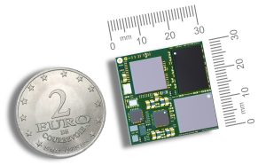
Toradex Launches Two New Computer on Module Families for Ultra-Compact Industrial and IoT Applications
Toradex has expanded its embedded computing portfolio with four new modules powered by NXP i.MX 93 and i.MX 91 processors: OSM iMX93, OSM iMX91, and Lino iMX93, Lino iMX91 by launching two entirely new Computer on Module (CoM) families, OSM and Lino.
The OSM and Lino families deliver cost-optimized, industrial-grade reliability, offering ultra-compact form factors, and long-term software support, designed for high-volume, space-constrained industrial IoT devices, like industrial controllers, gateways, smart sensors, and handheld systems, among others. For AI at the Edge, Industrial IoT applications, the NXP i.MX 93 offers a 0.5 TOPS NPU, enabling entry-level HW accelerated on-device machine learning for smart sensing, analytics, and industrial intelligence. Designed for extreme temperatures from -40°C to +85°C, both the OSM and Lino families deliver industrial-grade reliability and availability through 2038, providing a future-proof foundation for next-generation IoT and edge devices.
Both families deliver new compact, reliable, industrial Edge AI compute platforms”, said Samuel Imgrueth, CEO at Toradex. “While OSM adds a solderable standard form factor, Lino provides connector-based ease of use for rapid integration and serviceability. This empowers customers to design next generation, intelligent, space-constrained devices with confidence, scalability, and long-term support.
The OSM family adheres to the Open Standard Module (OSM) Size-S specification, providing a 30 × 30mm solderable, connector-less design optimized for automated assembly, rugged operation, and cost-effective scaling. It’s an ideal choice for high-volume applications up to several hundred thousand devices a year.

The Lino family provides a cost-optimized, connector-based entry point for space-constrained devices. Its easy-to-use connector interface simplifies integration, serviceability, and speeds up development, while rich connectivity options support a wide range of scalable industrial and IoT applications.

Toradex is also introducing the Verdin-Lino Adapter, allowing any Lino module to be mounted onto any Verdin-compatible carrier board. This gives customers immediate access to the powerful Verdin ecosystem and enables testing and validation using both the Verdin Development Board and existing Verdin-based custom designs.

All modules come with full Toradex Software support, including a Yocto Reference Image and Torizon support, a Yocto-based, long-term-supported Linux platform that provides secure OTA remote updates, device monitoring, remote access, and simplified EU CRA (Cyber Resilience Act) compliance. Its integration with Visual Studio Code and rich ecosystem accelerates development while ensuring production reliability and operational security. Torizon is also the ideal starting point for your own Linux Distribution.
The post Toradex Launches Two New Computer on Module Families for Ultra-Compact Industrial and IoT Applications appeared first on ELE Times.
Global IP dynamics highlight surging GaN innovation activity in Q3/2025, says KnowMade
🏰 Запрошуємо на екскурсію «Місто корупційних таємниць: відкрийте правду, яка ховається за фасадами»

14 грудня о 12:00 запрошуємо всіх охочих на екскурсію, яка змінить ваше уявлення про Київ.
Ми пройдемо маршрутами, які зберігають більше, ніж здається на перший погляд, повз будівлі, що могли б розповісти не одну цікаву історію.
The Great Leap: How AI is Reshaping Cybersecurity from Pilot Projects to Predictive Defense
Imagine your cybersecurity team as a group of highly-trained detectives. For decades, they’ve been running through digital crime scenes with magnifying glasses, reacting to the broken window or the missing safe after the fact. Now, suddenly, they have been handed a crystal ball—one that not only detects the threat but forecasts the modus operandi of the attacker before they even step onto the property. That crystal ball is Artificial Intelligence, and the transformation it’s bringing to cyber defense is less a technological upgrade and more a fundamental re-engineering of the entire security operation.
Palo Alto Networks, in partnership with the Data Security Council of India (DSCI), released the State of AI Adoption for Cybersecurity in India report. The report found that only 24% of CXOs consider their organizations fully prepared for AI-driven threats, underscoring a significant gap between adoption intent and operational readiness. The report sets a clear baseline for India Inc., examining where AI adoption stands, what organizations are investing in next, and how the threat landscape is changing. It also surfaces capability and talent gaps, outlines governance, and details preferred deployment models.
While the intent to leverage AI for enhanced cyber defense is almost universal, its operational reality is still maturing. The data reveals a clear gap between strategic ambition and deployed scale.
The report underscores the dual reality of AI: it is a potent defense mechanism but also a primary source of emerging threat vectors. Key findings include:
- Adoption intent is high, maturity is low: 79% of organizations plan to integrate AI/ML towards AI-enabled cybersecurity, but 40% remain in the pilot stage. The main goal is operational speed, prioritizing the reduction of Mean Time to Detect and Respond (MTTD/MTTR).
- Investments are Strategic: 64% of organizations are now proactively investing through multi-year risk-management roadmaps.
- Threats are AI-Accelerated: 23% of the organizations are resetting priorities due to new AI-enabled attack paradigms. The top threats are coordinated multi-vector attacks and AI-poisoned supply chains.
- Biggest Barriers: Financial overhead (19%) and the skill/talent deficit (17%) are the leading roadblocks to adoption.
- Future Defense Model: 31% of organizations consider Human-AI Hybrid Defense Teams as an AI transforming cybersecurity approach and 33% of organizations require human approval for AI-enabled critical security decisions and actions.
“AI is at the heart of most serious security conversations in India, sometimes as the accelerator, sometimes as the adversary itself. This study, developed with DSCI, makes one thing clear: appetite and intent are high, but execution and operational discipline are lagging,” said Swapna Bapat, Vice President and Managing Director, India & SAARC, Palo Alto Networks. “Catching up means using AI to defend against AI, but success demands robustness. Given the dynamic nature of building and deploying AI apps, continuous red teaming of AI is an absolute must to achieve that robustness. It requires coherence: a platform that unifies signals across network, operations, and identity; Zero-Trust verification designed into every step; and humans in the loop for decisions that carry real risk. That’s how AI finally moves from shaky pilots to robust protection.”
Vinayak Godse, CEO, DSCI, said “India is at a critical juncture where AI is reshaping both the scale of cyber threats and the sophistication of our defenses. AI enabled attacker capabilities are rapidly increasing in scale and sophistication. Simultaneously, AI adoption for cyber security can strengthen security preparedness to navigate risk, governance, and operational readiness to predict, detect, and respond to threats in real time. This AI adoption study, supported by Palo Alto Networks, reflects DSCI’s efforts to provide organizations with insights to navigate the challenges emerging out of AI enabled attacks for offense while leveraging AI for security defense.
The report was based on a survey of 160+ organizations across BFSI, manufacturing, technology, government, education, and mid-market enterprises, covering CXOs, security leaders, business unit heads, and functional teams.
The post The Great Leap: How AI is Reshaping Cybersecurity from Pilot Projects to Predictive Defense appeared first on ELE Times.
I know it's nothing crazy but I built this little FM radio board from a kit and I'm proud because it works. I've never soldered before so please don't mind my ugly soldering skills
 | submitted by /u/Cold-Helicopter6534 [link] [comments] |
Just wanted to share the insides of this Securesync 1200 signal generator from 2000s and the option card i installed
 | submitted by /u/jacobson_engineering [link] [comments] |
Bringing up my rosco m68k
 | Hey folks! On my boards the official firmware boots cleanly, the memory checks pass, and UART I/O behaves exactly as it should. I’m using the official rosco tools to verify RAM/ROM mapping, decoding, and the overall bring-up process. I also managed to get a small “hello world” running over serial after sorting out the toolchain with their Docker setup. I’m also tinkering with a 6502 through-hole version — something simple for hands-on exploration of that architecture. Happy to answer any questions or discuss the bring-up process. [link] [comments] |
Weekly discussion, complaint, and rant thread
Open to anything, including discussions, complaints, and rants.
Sub rules do not apply, so don't bother reporting incivility, off-topic, or spam.
Reddit-wide rules do apply.
To see the newest posts, sort the comments by "new" (instead of "best" or "top").
[link] [comments]
My first Smart Socket :)
") | submitted by /u/udfsoft [link] [comments] |
eth industrial switch rx/tx
 | yet still one pair leads to nonexisting chip and second shows only diagnostics from mcu. Life is brutal. [link] [comments] |
Simple Electronic Dice
 | I had a free evening, so decided to make this in the shed/workshop. It uses a 555 to produce rapid pulses, and a 4017 decade counter to sequence 6 LEDs rapidly. in r/askelectronics I asked for advice about more chips I can use in the future, and got another 4000 series which will allow me to drive a seven segment display in the same fashion, as opposed to six individual LEDs. Once I was happy with how the circuit behaves on the breadboard I put it to stripboard. I decided to current limit the white LEDs with a 12KR resistor. I don't know if using an opto-isolator in the way I did is good practice or not. It works, and is simple enough. I found that for me, the best way to use a pulldown resistor for the 4017 trigger was to also connect a small .1uF ceramic capacitor in parallel to the pulldown resistor. I know that by no means is this groundbreaking, or advanced. It's probably akin to something that would have been made 30 or 40 years ago, but I only dabble as a hobby, and find soldering away, alone, for a few hours, whilst the rain hammers down outside quite therapeutic for me. [link] [comments] |
Nice work!
 | submitted by /u/Electro-nut [link] [comments] |
EEVblog 1723 - AlienTek DM40 Multimeter/Oscilloscope Review
Зустріч із данськими організаціями

🇺🇦🇩🇰 У КПІ ім.
onsemi releases EliteSiC MOSFETs in T2PAK top-cool package
Без київських політехніків Україна не була б повноправним членом Антарктичного клубу

Величезним досягненням української науки сьогодні, на думку професійної спільноти, є продовження антарктичних досліджень на станції "Академік Вернадський" та океанографічному судні "Ноосфера". З гордістю можемо сказати, що випускники і вчені КПІ є учасниками як отримання станції Україною майже 30 років тому, так і забезпечення її життєдіяльності та виконання програми спостережень нині.
My class AB amplifier
 | So, I'm developing a guitar amplifier for a friend, and I need a high power (as for my standards) amp to make it loud. So I made this one, the most powerful discrete amp to date, that can deliver 20Vpp to 8 ohm speaker without distortion at 24V supply. I had a problem with connecting everything for tests and idle current calibration because PCB is , so i had to improvise. I put a power diode into ground terminal of amp, connected a big clip of function generator ground, then connecred small clip of power supply ground, and scope ground to power supplu ground clip. The effect is this big tangle of wires and connectors, but it worked as intended. The design is a variation of amp from 70s record player but with changed voltage rating and conversion from class B to AB. It's suprisingly stable and silent when input is floating, so I like it. [link] [comments] |
The Big Allis generator sixty years ago

Think back to the 1965 electrical power blackout in the Northeast United States of just over sixty years ago. It was on November 9, 1965. There was a huge consequence for Consolidated Edison in New York City.
Their power-generating facility in Ravenswood had been equipped with a generator made by Allis-Chalmers, as shown in the following screenshots.

Figure 1 Ravenswood power generating facility and the Big Allis power generator.
That generator was the largest of its kind in the whole world at that time. Larger generators did get made in later years, but at that time, there were none bigger. It was so big that some experts opined that such a generator would not even work. Because of its size and its manufacturer’s name, that generator came to be called “Big Allis”.
Big Allis had a major design flaw. The bearings that supported the generator’s rotor were protected by oil pumps that were powered from the Big Allis generator itself.
When the power grid collapsed, Big Allis stopped delivering power, which then shut down the pumps delivering the oil pressure that had been protecting the rotor bearings.
With no oil pressure, the bearings were severely damaged as the rotor slowed down to a halt. One newspaper article described the bearings as having been ground to dust. It took months to replace those bearings and to provide their oil pumps with separate diesel generators devoted solely to maintaining the protective oil pressure.
So far as I know, Big Allis is still in service, even through the later 1977 and 2003 blackouts, so I guess that those 1965 revisions must have worked out.
John Dunn is an electronics consultant, and a graduate of The Polytechnic Institute of Brooklyn (BSEE) and of New York University (MSEE).
Related Content
- Modern Distribution Grid Technologies
- Power grid blackouts: Are they preventable and predictable?
- Teardown: The power inverter – from sunlight to power grid
- Inventions that were almost ahead of their time
The post The Big Allis generator sixty years ago appeared first on EDN.
Сторінки


![[link]](https://i.redd.it/uuukn3f0vw5g1.png)
![[link]](https://i.redd.it/cali7yzmcj5g1.jpeg)
![[link]](https://i.redd.it/u71wacfmwg5g1.jpeg)