
Збирач потоків
6G Development: Turning 5G’s Roadblocks into Future Opportunities
The global rollout of 5G was expected to be transformative, providing blazing-fast speeds with incredibly low latencies. Through quite visionary and futuristic applications, 5G would have helped in applications such as autonomous driving and telemedicine.
Having made some progress, the realization has often been short of early expectations. Many industries have yet to create palpable value, whilst those in the operator’s arena are facing the challenge of recovering massive investments made in 5G infrastructure.
Now, with accelerated 6G research, the telecom industry has undergone an unusual opportunity to address these shortfalls and, learning from the trials of 5G, set engineers and innovators on the path of designing a wireless future that is smarter, better, and more inclusive.
Key Lessons from 5G Adoption
- Too Much Promises, Not Enough Delivery
The hype around 5G had fueled expectations for revolutionary new applications. Mobile broadband speeds improved, yet many flagship applications-think massive IoT or mission-critical ultra-reliable low-latency communications (URLLC)-have not scaled in the way expected. Particularly hesitant are enterprises, leaving operators holding significant investments but slowly gaining returns.
- Deployment Complexity
Deployment from 4G to 5G was further complicated than expected. Small cell deployments for (mmWave) frequencies, spectrum allocation complications, and the very expensive upgrades to various parts of networks caused more delays in the commercial rollout. While the 5G core gave operators and enterprises a lot of flexibility, operational costs also increased, along with deployment time, to their aggravation.
- Ecosystem Gaps
Like in many solutions, 5G has been held back by its ecosystem. The smartphones were fast to adapt, while industrial IoT and other enterprise-critical devices took their own sweet time. Unable to muster an ecosystem of applications, services, and devices, industries were left unable to embrace 5G fully-or monetize it.
How 6G Aims to Deliver Where 5G Fell Short
Building on a Stronger Foundation
There is no point in going back to the drawing board for 6G. It is a natural evolution of the 5G capabilities. Enhancements to (eMBB), massive IoT, and URLLC will come alongside AI-native and machine-learning-driven networks, making such systems smarter, more reliable, and adaptable to the real world such as AR, industrial automation, and connected healthcare.
Simplifying Network Complexity
One of the intended goals of 6G is to ease all network operations. Simplifying the core architecture will make deployment much faster, cheaper, and easier to manage; operators and enterprises now have fewer barriers.
Expanding the Ecosystem
Taking note of the slow ecosystem development in 5G, 6G R&D now places device and application readiness alongside infrastructure. This, in turn, means that industries will have the hardware and software required to harness the capabilities of 6G from day one, thus speeding up adoption in manufacturing, logistics, healthcare, and transportation.
Smarter Spectrum Utilization
6G will scale spectrum efficiency on top of any mmWave operations into upper mid-band (7–24 GHz) and terahertz ranges. This means that it can deliver faster data throughput, lower latency, and wider coverage, higher on spectrum-sharing issues that made 5G under-perform in densely populated urban setups.
Sustainability and Equity
Of course, spacetime performance will identify markets on energy-efficient and global-inclusive standards. By limiting power usage and operational footprints, 6G will be geared towards sustainability. At the same time, they aim to extend reliable connectivity to underserved regions, narrowing the digital divide.
Testing’s Contribution to 6G Success
Testing that is precise, adaptable, and standards-based will be essential to the deployment of 6G. In addition to verifying 6G capabilities, tools must also guarantee 5G backward compatibility. More significantly, collaborations with skilled testing suppliers will contribute to ensuring seamless development cycles, adherence to regulations, and practical performance.
Conclusion:
In conclusion, 6G presents an opportunity to address 5G’s drawbacks by emphasising sustainability, ecosystem preparedness, and pragmatism. The upcoming ten years provide engineers, operators, and businesses the chance to transform wireless communication into something quicker, easier, and more significant for communities and industries around the globe.
(This article has been adapted and modified from content on Anritsu.)
The post 6G Development: Turning 5G’s Roadblocks into Future Opportunities appeared first on ELE Times.
Vishay Ametherm SL2220007 Inrush Current Limiting NTC Thermistor Receives UL Recognition
Certified by UL Solutions, Device Is Verified to Meet Stringent Safety and Performance Requirements
Vishay Intertechnology, Inc. announced that its Vishay Ametherm SL2220007 bigAMP inrush current limiting negative temperature coefficient (NTC) thermistor has received UL certification. The certification process—conducted by UL Solutions under File E209153, Volume 1—verified that the SL2220007 thermistor complies with the stringent UL Mark requirements for safety and performance.
“Achieving UL recognition for the SL2220007 is an important milestone that underscores our commitment to delivering high performance, safety-verified solutions,” said Eric Rauch, VP Vishay Ametherm at Vishay Intertechnology. “UL certification is a trusted benchmark worldwide. The UL Mark on the SL2220007 gives our customers added assurance that the thermistor meets the highest standards for quality, safety, and reliability for their most demanding power designs.”
The SL2220007 offers a steady-state current of 7 A while maintaining rugged reliability and long-term performance. Optimized for switching power supplies, AC motors, uninterruptible power supplies (UPS), industrial inverters, and variable frequency drives, the thermistor protects circuits by absorbing high inrush current when equipment is first powered on. It provides high initial resistance that quickly drops to a negligible level as steady-state current begins to flow, enabling the device to handle up to 125 J of energy and 265 VRMS of voltage with minimal power loss.
The post Vishay Ametherm SL2220007 Inrush Current Limiting NTC Thermistor Receives UL Recognition appeared first on ELE Times.
Infineon CoolGaN technology boosts power performance in network PoE applications of Universal Microelectronics
Infineon Technologies AG provides CoolGaN power transistors to Universal Microelectronics Co., Ltd. (UMEC) for the company’s new 250 W adapter for networking Power over Ethernet (PoE) applications. Infineon´s CoolGaN transistors enable reliable, high-performance solutions and help UMEC develop safer and energy-efficient technology to address modern power system challenges. These solutions are ideal for power electronics across various industries, including telecommunications, industrial electronics, medical technology, and consumer electronics.
GaN-based power devices provide higher efficiency, reducing heat generation and energy consumption. They can operate at higher frequencies and power densities, enabling more compact designs, maximizing rack space utilization, and improving cooling in AI data centers, for example. Furthermore, reducing system size allows for more hardware content and improved air flow, which results in less wasted heat and ultimately decreases operational costs and the overall carbon footprint.
“We are excited to see our CoolGaN technology powering UMEC’s new 250 W adapter for networking applications. This collaboration demonstrates the potential of GaN to revolutionize the data center industry, enabling smaller, more efficient, and reliable power solutions,” says Johannes Schoiswohl, Head of GaN Business Line at Infineon.
“Partnering with Infineon and utilizing their CoolGaN power transistors in our new 250 W adapter has allowed us to create a product that delivers exceptional efficiency and reliability,” says Richard Lin, Power Supply Product Manager at Universal Microelectronics. “This innovation aligns with our commitment to developing cutting-edge electronic solutions that meet the evolving demands of the networking industry.”
UMEC’s 250 W adapter offers excellent efficiency of 95 percent, a power density increase of around 39 percent. The CoolGaN transistors reduce power losses, enable switching at frequencies above 200 kHz, and improve thermal behavior, which is critical for compact and high-density power supplies. These are critical performance improvements in the global virtual networking market, which is expected to grow from $48.6 billion in 2024 to approximately $200 billion by 2030, at a CAGR of 26.5 percent.
Infineon’s gallium nitride power transistors are driving digitalization and decarbonization, while enabling high-frequency operation, increasing efficiency and reducing system size in a wide range of applications. They are available in voltage classes from 60 V to 700 V and in a broad variety of packages.
The post Infineon CoolGaN technology boosts power performance in network PoE applications of Universal Microelectronics appeared first on ELE Times.
EEVblog 1709 - Mailbag: Haasoscope Pro USB Oscilloscope
Infineon Debuts Pair of Rugged MEMS Microphones for Harsh Environments
Lumentum presenting at ECOC 2025
Видавничий дім КПІ ім. Ігоря Сікорського

Видавничий дім КПІ ім. Ігоря Сікорського – одне з осередь української та світової наукової думки.
AMD Aims New Embedded Processors at Low-Latency Edge Designs
RTX unveils APG-82(V)X radar enhanced with gallium nitride
PWM buck regulator interface generalized design equations

A while back, I published the Design Idea (DI) “Simple PWM interface can program regulators for Vout < Vsense.” It showed some simple circuits for PWM programming of standard bucking-type regulator chips, both linear and switching, including applications that need an output voltage span that can swing well below the regulator’s sense voltage.
Wow the engineering world with your unique design: Design Ideas Submission Guide
Recent reader comments have shown interest in applying those designs to different applications and regulators. So, here’s a step-by-step procedure to make that process easier.
Note that it only works if Vx > 2Vs and Vl > Vs.
 Figure 1 Ten discrete parts comprise a circuit for linear regulator programming with PWM.
The steps are:
- Vs = U1 sense voltage from U1 datasheet (typically 0.5 to 1.25 V)
- Vl = available logic rail (typically 3 to 5 V)
- Vx = desired maximum output voltage at PWM duty factor = 100%
- Vpp = PWM peak to peak amplitude, typically Vl
- Fp = PWM rep rate
- N = PWM bits of resolution, N > 4
- R1 = recommended value from U1 datasheet example application
- R2 = R1(Vx/Vs – 1)
- R4 = R2Vl/Vs – R1 – R2
- R5 = (Vl – Q2vbe)Q2minbeta(R4 + R1 + R2)/Vl
- R3 = Vpp/(Vs/R1 + (Vl – Vs)/(R1 + R4))
- R3C3 = R2C2 = 2((N-2)/2)Fp-1
- C1 = C2R2/R1
Now, taking the inexpensive XLsemi XL4016 asynch buck converter as an example case for U1, and turning the crank for these givens gives you:
- Vs = 1.25 V
- Vl = 3.3 V
- Vx = 30 V
- Vpp = 3.3 V
- Fp = 10 kHz
- N = 8
- R1 = recommended value from U1 datasheet figure 4 = 3.3 kΩ
- R2 = 75 kΩ
- R4 = 120 kΩ
- R5 = 15 MΩ
- R3 = 8.2 kΩ
- C3 = 0.1 µF, C2 = 0.011 µF
- C2 = 0.27 µF
This yields Figure 2.

Figure 2 General design-accommodating parameters listed above. Note that U1-specific parts (e.g., inductor, capacitors, and power diode) are not shown.
Note that if the microamps and millivolts of residual zero offset that persist on the unloaded supply output at PWM = zero duty factor aren’t objectionable, then the Q2 R5 current sink is irrelevant and can be omitted.
Stephen Woodward’s relationship with EDN’s DI column goes back quite a long way. Over 100 submissions have been accepted since his first contribution back in 1974.
Related Content
- Simple PWM interface can program regulators for Vout < Vsense
- Revisited: Three discretes suffice to interface PWM to switching regulators
- Three discretes suffice to interface PWM to switching regulators
- Cancel PWM DAC ripple with analog subtraction
- Add one resistor to allow DAC control of switching regulator output
The post PWM buck regulator interface generalized design equations appeared first on EDN.
Aixtron ships its 100th G10-SiC system
Handling Signal Swings: Wide Common Mode Range in Action
Communication between devices must be reliable in modern industrial, automotive, and energy applications. Yet, engineers often encounter strange situations where everything seems to be connected well but the networks start acting strange out there in the field. Intermittent loss of communication and unexpected breakdown of nodes become tremendously expensive issues-a major reason for frustration, for such problems hardly pop their heads in the lab.
After more research, it is discovered that the sneaky evil is common mode voltage swings brought on by external circumstances. The swings push the signal outside the limits set in the original RS-485 standard, thereby maring the data exchange. Today’s extended CM range RS-485 transceivers are meant to protect networks against such eventualities.
When Noise Invades the Network

Figure 1: Scope Trace
A plain scope probe can narrate a grand story. At 500 kHz, it is not unusual to observe differential signals severely distorted due to external coupling. The transceiver receives data swathed in extraneous noise, and communication becomes unstable.
The 1983 EIA-485 standard provided for such situations by specifying a large common mode voltage range of -7 V to +12 V. Theoretically, this would be safe for signals. Practically, long cable lengths, wire resistance, and common mode external interference can move common mode levels far beyond that range.
Sources of Common Mode Swings:
A number of real-world conditions can inject interference currents into RS-485 networks:
- Motors and High-Voltage Power Supplies

Figure 2: Common Mode Swing Sources – Motors and High Voltage Power Supplies
Motors used in industry and switching power supplies produce powerful electromagnetic fields. These fields tend to couple readily into surrounding cabling, inducing unwanted RF interference on the data lines.
- Power and Data Bundled Together
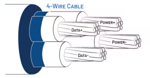
Figure 3: Common Mode Swing Sources – Cables with Power and Data Bundled Together
Running AC power cables alongside RS-485 data cables within the same cable causes capacitive coupling, which injects currents directly into the communication network.
- Ground Potential Differences Between Buildings

Figure 4: Common Mode Swing Sources – Ground Potential Differences Between Buildings

Figure 5: Ground Voltage Differences Explained
When networking across buildings, ground potential differences can create large voltage shifts. Leakage currents from safety grounds or neutral wiring often raise the common mode voltage, pushing it outside the RS-485 tolerance.
Why Extended Common Mode Range Transceivers Help
Rather than depend solely on costly shielded cables, a better solution is to implement RS-485 transceivers that have wider common mode ranges. These chips are designed to maintain reliable data transfer even when external noise forces voltages well outside the legacy standard.
Examples include:
MAX33070E – MAX33074E: Half-duplex, 3.3 V to 5 V products with ±40 V common mode tolerance
LTC2862A and LTC2863: Half- or full-duplex products with improved noise immunity
Through the implementation of these resilient solutions, engineers are able to safeguard networks against downtime, minimize field failures, and lengthen the lifespan of industrial systems.
Conclusion:
Installing and operating RS-485 networks under regulated settings is nearly impossible. Motors, power supplies, bundled cables-if anything-shift voltages around in ways that disrupt communication.
With that said, the way to go will be to design with extended common mode range transceivers that offer a safety margin against any such disruptive swings and thus ensuring communication stays steady and reliable even in the harshest industrial weather.
(This article has been adapted and modified from content on Analog Devices.)
The post Handling Signal Swings: Wide Common Mode Range in Action appeared first on ELE Times.
Infineon’s CoolGaN power transistors incorporated into Universal Microelectronics’ 250W adapter for networking PoE applications
How Cloud-Integrated Printing is Revolutionizing Automotive Manufacturing
The automotive landscape has been witnessing a technological renaissance. Apart from EVs and autonomous driving, a quieter but profound change has been occurring: cloud-integrated printing. Hence, from rapid 3D prototyping to digitized supply chain management, cloud-based printing is defining new constraints in vehicle design, manufacturing, and maintenance. Analysts estimate an injection of unprecedented growth in the global cloud printing in the automotive market between 2025 and 2034; in turn, billions of dollars-worth of opportunities shall be disclosed. This means that the transformation is not only about efficiency but about sustainability, agility, and rethinking the whole concept of a factory floor for manufacturers.
Cloud Printing: With cloud printing being a mainstay of office workflows, it has now become central to automotive production. Merging next-generation hardware with managed services and cloud-based software, automotive firms can:
- Prototype cars at unprecedented velocities.
- Label and track thousands of parts globally across diverse supply chains.
- Digitize technical manuals, blueprints, and marketing collateral.
- Streamline workflows between manufacturing plants around the globe.
The cloud layer introduces a revolutionary aspect: frictionless integration anywhere, elastic production, and secure protection of sensitive designs with private or hybrid cloud models.
Market Highlights:
- North America: Holds its 30% market share in 2025 underpinned by high EV uptake and top OEMs such as Tesla, Ford, and Rivian.
- Asia-Pacific: Set to experience the quickest growth by 2034 with China, Japan, and India’s growing automotive and EV industries.
- Hardware vs. Software: Hardware has a commanding 45% market share, but cloud-based software platforms are swiftly catching up.
- Printing Types: 2D printing comprises 55% of use, but 3D printing is becoming the real growth driver.
- Applications: Parts labeling and traceability dominate, but cloud-based vehicle prototyping is the most rapidly increasing segment.
- Deployment Models: Private cloud adoption holds steady at 50%, although hybrid solutions are quickly gaining traction.
- End-Users: OEMs account for 60% of adoption, with manufacturers increasingly using 3D printing for sophisticated parts.
Trends Driving Adoption:
- Collaboration and Partnerships: Partnerships are driving faster adoption. As an example, Sharp collaborated with directprint.io in February 2025 to grow cloud printing solutions throughout the UK.
- AI-Driven Printing: AI is becoming more and more integrated into cloud platforms. Infosys and Telstra Group’s August 2025 partnership in Australia shows how machine learning is powering smarter manufacturing workflows.
- Regional Hardware Expansion: To address booming demand, Seiko Epson and other firms are increasing production, with the company opening a large-capacity printer plant in Chennai, India, in July 2025.
Hardware and Software:
Though hardware such as 3D printers and high-end scanners are seen as visible drivers of innovation, software is emerging as the real differentiator:
- Hardware: Facilitates custom part fabrication, sophisticated prototyping, and aids EV component manufacturing.
- Software: Cloud-based design systems and additive manufacturing software simplify vehicle design, enable better traceability, and enhance operational effectiveness.
2D vs. 3D Printing:
- 2D Printing: Remains the vital use cases such as documentation, blueprints, and marketing material.
- 3D Printing: The game-changer, facilitating lightweight EV components, on-demand spare parts, and quicker prototyping cycles, with growth outpacing all other segments.
Applications Driving Market Growth:
- Parts Labeling & Traceability: Critical to supply chain transparency and regulatory compliance.
- Vehicle Prototyping & Design: The most rapidly growing segment, owing to cloud-based 3D prototyping speeding up the design-to-production process.
Deployment Models: Private vs. Hybrid Cloud:
- Private Cloud: Provides control, customization, and security for proprietary IP.
- Hybrid Cloud: Fuses scalability, cost-effectiveness, and effortless data management, emerging as the preferred model for contemporary EV ecosystems.
Leading the Adoption Curve:
- OEMs represent 60% of all adopting for innovation and authentic part quality maintenance.
- In the rise: Tier-1 and 2 suppliers are increasingly turning to cloud print, particularly 3D printing, for easy and complex methods of cost-efficient part production.
Regional Outlook:
- North America as a powerhouse: Leader in cloud print adoption driven by EVs and tech-conscious OEMs.
- Asia Pacific: As fastest-growing, is nurtured by China’s EV boom and by Japan’s mature component design, with India gearing up to be an automotive manufacturing and R&D hub. Such expansions as the May 2025 launch of Konica Minolta in Australia exemplify this recent flow of energy into the region.
The Way Forward:
In the very next ten years, automotive manufacturing will be redefined. Cloud-integrated printing is more than just a tool of productivity-it stands for sustainability, innovation, and agile transformation. As 3D, AI, and hybrid cloud models converge, automakers and suppliers would rather become active in shaping the industry rather than playing catch-up.
Going Cloud-Integrated Printing today means setting the standards of tomorrow for automotive innovation.
(This article has been adapted and modified from content by Laxmi Narayan, Research Analyst, Towards Automotive.)
The post How Cloud-Integrated Printing is Revolutionizing Automotive Manufacturing appeared first on ELE Times.
A crash course in 3D IC technology

What’s 3D IC, and what’s causing the shift from 2D IC to 3D IC? How does this new technology relate to heterogeneous integration and advanced packaging? What is required for a successful 3D IC implementation? EDN recently published a three-article series to cover multiple facets of this advanced packaging technology.
Below is a sneak peek at this three-article series, which explains 3D IC fundamentals, microarchitectures, toolkits, and design use cases.
Part one, titled “Making your architecture ready for 3D IC”, provided essential context and technical depth for design engineers working toward highly integrated, efficient, and resilient 3D IC systems. It explains 3D IC microarchitectures that redefine how data and controls move through a system, how blocks are partitioned and co-optimized across both horizontal and vertical domains, and how early-stage design decisions address the unique challenges of 3D integration.
Making your architecture ready for 3D IC
Part two, titled “Putting 3D IC to work for you”, outlines the challenges and opportunities in adopting 3D IC technology. It demonstrates how 3D IC enables efficient chiplet integration and reuse, accelerates innovation, and guarantees manufacturability across organizational boundaries. The article also provides a detailed examination of 3D IC design toolkits and workflows, as well as their incorporation of AI technology.
The third and final part, titled “Automating FOWLP design: A comprehensive framework for next-generation integration”, presents fan-out wafer-level packaging (FOWLP) as a case study, showing how automation frameworks manage the inherent complexity of advanced packaging and the scale of modern layouts, racking up millions of pins and tens of thousands of nets. It also demonstrates how effective frameworks promote collaboration among package designers, layout specialists, signal and power integrity analysts, and thermal and mechanical engineers.
Automating FOWLP design: A comprehensive framework for next-generation integration
Related Content
- 3D IC Design
- Thermal analysis tool aims to reinvigorate 3D-IC design
- Heterogeneous Integration and the Evolution of IC Packaging
- Tighter Integration Between Process Technologies and Packaging
- Advanced IC Packaging: The Roadmap to 3D IC Semiconductor Scaling
The post A crash course in 3D IC technology appeared first on EDN.
CEA-Leti and CRHEA present step toward full-color AR/VR micro-displays at MicroLED Connect Conference
✅ Оголошується конкурс на заміщення посад
Національний технічний університет України "Київський політехнічний інститут імені Ігоря Сікорського" оголошує конкурс на заміщення вакантних посад. Термін подання документів до 26.10.2025 року.
Конкурс на заміщення вакантної посади завідувача кафедри
Конкурс на заміщення вакантних посад професорів
Конкурс на заміщення вакантних посад доцентів, викладачів
Photon Design exhibiting product range at ECOC 2025
Socomec Launches COUNTIS P new range of Smart AC/DC Energy Meters for Efficient Energy Management
From design to commissioning, Socomec guarantees high-performance, sustainable electrical installations
Socomec announced the launch of its latest innovation: COUNTIS P, a next-generation range of smart energy meters designed to meet the evolving needs of modern infrastructure. With over three decades of industry expertise, this launch reinforces Socomec’s commitment to innovation, sustainability, and excellence in energy efficiency and digital transformation.
Mr. Meenu Singhal, Regional Managing Director – Greater India, Socomec Innovative Power Solutions, emphasized the significance of the launch, stating, “As the energy consumption becomes increasingly complex across sectors, organizations are under pressure to manage usage more efficiently while ensuring compliance and sustainability. COUNTIS P offers a smarter, simpler way to manage energy through its compact design, AC/DC compatibility, and seamless integration with digital platforms. It empowers businesses to gain real-time insights, improve cost allocation, and drive meaningful progress toward energy efficiency goals”. He stated that this innovation demonstrates Socomec’s ongoing efforts to deliver intelligent, sustainable solutions that support customers in navigating today’s energy challenges while preparing for tomorrow’s opportunities.
The COUNTIS P range delivers precision metering, modular design, and advanced connectivity, including Modbus RTU/TCP protocols. Designed for versatility, COUNTIS P is compatible with both AC and DC systems and operates seamlessly across single-phase and complex three-phase networks. Built to perform in harsh environments, it maintains high accuracy even under extreme temperature conditions. Its plug-and-play QuickConnect installation simplifies deployment, reducing time and complexity for installers and integrators.
When integrated with Socomec’s digital monitoring platforms, COUNTIS P provides real-time energy insights that help customers track consumption, identify inefficiencies, make data-driven decisions, reduce operational costs, and support their sustainability goals. These capabilities make COUNTIS P a future-ready solution for organizations looking to optimize energy use and meet tightening regulatory standards.
In many sectors, managing sub-billing remains a critical challenge. Accurate sub-metering enables fair and transparent rebilling of energy consumption across tenants or business units. COUNTIS P meters are MID-certified, ensuring reliable accuracy and full compliance with regulatory requirements. This makes them an ideal solution for organizations seeking to avoid billing errors and ensure transparency in energy cost allocation. With features like QuickConnect technology, AC/DC compatibility, and MID certification, COUNTIS P is ideal for buildings, industry, infrastructure, and EV charging stations.
Socomec supports its customers throughout the entire lifecycle — from design to commissioning — ensuring high-performance, compliant, and sustainable electrical installations. As energy consumption becomes a critical issue for businesses, reducing kilowatt-hour usage not only lowers costs but also minimizes environmental impact. In this context, COUNTIS P stands out as a smart, reliable, and efficient tool for modern energy management.
The post Socomec Launches COUNTIS P new range of Smart AC/DC Energy Meters for Efficient Energy Management appeared first on ELE Times.
Setting Up PCM and I2S Formats for Reliable SCO Loopback Transmission
In the contemporary wireless audio industry, providing crystal-clear uninterrupted sound is such a major and recurrently faced problem. Depending on the nature of Bluetooth headsets ethereally connecting with other apparatus modules over wireless ambience or in the car for in-roads communication purposes, or in gaming devices, it is imperative that, from the engineers’ standpoint, audio signals need to stay unstuck from distortion. To validate and optimize further, SCO (Synchronous Connection-Oriented) loopback transmissions can be put to use.
In this manual, loopback mode is described. Why do we need loopback testing in Bluetooth audio? And how does one configure PCM or I2S for an SCO loopback using the Infineon AIROC Bluetooth controllers?
What is a Loopback Mode?
Loopback mode is a constraint and verification method for wireless audio. Rather than train the audio signal back to a set destination (e.g., speakers, headphones, etc.), the signal is looped back to the originating source. This allows the developers to check the signal quality, such as verifying hardware configurations and troubleshooting towards identifying any mismatch, without dependence on external devices for tests.
Normal vs. Loopback Mode:
Normal Mode: Audio is transmitted to the output device.
Loopback Mode: Audio is redirected back to the source for testing.
Test Environment
To configure SCO loopback transmission, you’ll need:
AIROC CYW20706 headset demo (PCM_OUT source) → GitHub demo project
Linux mbt tool for HCI command input → GitHub mbt tool
AIROC CYW89072 (or any supported Infineon Bluetooth controller) with firmware
Step-by-Step Setup for SCO Loopback Transmission
Step 1: Program the CYW20706 and Bring Up the Demo
- Flash the CYW20706 using ModusToolbox.
- Use the client control tool to run the demo.
- Pair a phone with the CYW20706 and start playback.
Step 2: Connect Hardware
Wire the CYW20706 PCM_OUT pin to the CYW89072 PCM_IN pin.
Step 3: Download Firmware
./mbt download [filename].hcd –minidriver
Step 4: Enable Loopback Mode
./mbt input_command 24fc0101
PCM Configuration
8K PCM
./mbt input_command 1cfc050001000101
./mbt input_command 24fc0101
16K PCM
./mbt input_command 7efc03010200
./mbt input_command 6dfc0400010102
./mbt input_command 1cfc050002000101
./mbt input_command 1efc050000030000
./mbt input_command 24fc0101
I2S Configuration
8K I2S
./mbt input_command 7efc03000200
./mbt input_command 6dfc0401010001
./mbt input_command 24fc0101
16K I2S
./mbt input_command 7efc03010200
./mbt input_command 6dfc0401010102
./mbt input_command 24fc0101
Pin Configuration Notes
For controllers like CYW555xx or CYW43xx, an additional command may be required to route PCM/I2S to default pins:
./mbt input_command 61fc0501b9b8b8b8
By default, the setup assumes TDM2 pins are in use. If you are using alternative pins, adjust the commands accordingly.
Key Takeaway
SCO loopback transmission is an invaluable tool for validating wireless audio performance. By configuring PCM or I2S formats with Infineon’s AIROC Bluetooth controllers, engineers can easily verify signal integrity, fine-tune system performance, and ensure a smooth end-user audio experience.
(This article has been adapted and modified from content on Infineon Technologies.)
The post Setting Up PCM and I2S Formats for Reliable SCO Loopback Transmission appeared first on ELE Times.
Сторінки

