
Збирач потоків
Weekly discussion, complaint, and rant thread
Open to anything, including discussions, complaints, and rants.
Sub rules do not apply, so don't bother reporting incivility, off-topic, or spam.
Reddit-wide rules do apply.
To see the newest posts, sort the comments by "new" (instead of "best" or "top").
[link] [comments]
Візит партнерів задля впровадження освітньої програми з гуманітарного розмінування

Проректор КПІ ім. Ігоря Сікорського з міжнародних зв'язків Андрій Шишолін, директорка Навчально-наукового інституту енергозбереження та енергоменеджменту КПІ Оксана Вовк і директорка Українсько-Японського центру КПІ Катерина Луговська зустрілися 16 грудня з фахівцем з комунікацій Управління ООН з обслуговування проєктів (UNOPS) Михайлом Туряницею та журналісткою Інформаційного агентства "Кіодо-Ньюз" Нарумі Татеди (Японія).
Легенди КПІ у Лізі Легенд ГУР

З 20 листопада по 1 грудня 2025 року Головне управління розвідки Міністерства оборони України спільно з компанією HackenProof провели онлайн-змагання "Перший національний CTF". Участь у них взяла і команда dcua НН ФТІ КПІ ім. Ігоря Сікорського, яка показала найкращий результат – зайняла перше місце у найвищому рівні змагань – спеціальному заліку Ліги Легенд!
III-V Epi exhibiting at Photonics West 2026
Lumentum showcasing ultrafast and UV laser platforms for precision manufacturing
На війні загинув випускник нашого університету — Цапок Андрій Михайлович

🕯 З глибоким сумом повідомляємо, що Цапок Андрій Михайлович, випускник 2018 року Навчально-наукового механіко-машинобудівного інституту кафедри лазерної техніки та фізико-технічних технологій, загинув, захищаючи Україну.
Zero maintenance asset tracking via energy harvesting
Real-time tracking of assets has enabled both supply chain digitalization and operational efficiency leaps. These benefits, driven by IoT advances, have proved transformational. As a result, the market for asset-tracking systems for transportation and logistics firms is set to triple, reaching USD 22.5 billion by 2034¹. And, if we look across all sectors, the asset tracking market is forecasted to grow at a CAGR of 15%, reaching USD 51.2 billion by 2030².
However, the ability for firms to maximize the benefits of asset tracking is being constrained by the finite power limitations of a single component, the battery. Reliance on batteries has a number of disadvantages. In addition to the battery cost, battery replacement across multiple locations increases operational costs and demands considerable time and effort.
At the same time, batteries can cause system-wide vulnerabilities. When a tag’s battery unexpectedly fails, for example, a tracked item can effectively disappear from the network and the corresponding data is no longer collected. This, in turn, leads to supply chain disruptions and bottlenecks, sometimes even production line downtime, and reduces the very efficiencies the IoT-based system was designed to deliver (Figure 1).
![]()
Figure 1 Real-time tracking of assets is transforming logistics operations, enabling supply chain digitalization and unlocking major efficiency gains.
Battery maintenanceA “typical” asset tracking tag will implement two core functions: location and communications. For long-distance shipping, GPS will primarily be used as the location identifier. In a logistics warehouse, GPS coverage can be poor, but Wi-Fi scanning remains an option. Other efficient systems include FSK or BLE beacons, Wirepas mesh, or Quuppa’s angle of arrival (AoA).
For data communication, several protocols are possible,
- BLE if the assets remain indoors
- LTE-M if global coverage is a key requirement, and the assets are outdoors
- LoRaWAN if seamless indoor and outdoor coverage is needed, as this can use private, public, community, and satellite networks, with some of them offering native multi-country coverage.
Sensors can also improve functionality and efficiency. For example, an accelerometer can be added to identify when a tag moves and then initiate a wake-up. Other sensors can determine a package’s status and condition. In the case of energy harvesting, the power management chip can indicate the amount of energy that is available. Therefore, the behavior of the device can also be adapted to this information. The final important component on the board of an asset tracker will be an energy-efficient MCU.
The stated battery life of a 15-dollar tag will often be overestimated. This will mainly be due to the radio protocol behaviors. But even if the battery cost itself is limited, the replacement cost can be estimated at around 50 dollars once man-hours are factored into this.
An alternative tag based on the latest energy harvesting technology might have an initial cost of around 25 dollars, but with no batteries to replace, its total cost over a decade remains essentially the same, whereas even a single battery replacement already pushes a 15-dollar tag above that level.
For example, in the automotive industry, manufacturers transport parts using large reusable metal racks. Each manufacturer will use tens of thousands of these, each valued at around 500 dollars. We have been told that, because of scanning errors and mismanagement, up to 10 percent go missing each year.
By equipping racks with tags powered from harvested energy, companies can create an automated inventory system. This results in annual OPEX savings that can be in the order of millions of dollars, a return on investment within months, and lower CAPEX since fewer racks are required for the same production volume.
Self-powered trackingUnlike battery-powered asset trackers, Ambient IoT tags use three core blocks to supply energy to the system: the harvester, an energy storage element, and a power management IC. Together, these enable energy to be harvested as efficiently as possible.
Energy sources can range from RF through thermoelectric to vibration, but for many logistics and transport applications, the most readily available and most commonly used source is light. And this will be natural (solar) or ambient, depending on whether the asset being tracked spends most of its life outdoors (e.g., a container) or indoors (e.g., a warehouse environment).
For outdoor asset trackers on containers or vehicles, significant energy can be harvested from direct sunlight using traditional photovoltaic (PV) amorphous silicon panels. When space is limited, monocrystalline silicon technology provides a higher power density and still works well indoors. For indoor light levels, in addition to the traditional amorphous silicon, there are three additional technologies that become available and cost-effective for these use cases.
- Organic photovoltaic (OPV) cells can provide up to twice the power density of amorphous silicon. Furthermore, the flexibility of these PV cells allows for easy mechanical implementation on the end device.
- Dye-sensitized solar cells bring even higher power densities and exhibit low degradation levels over time, but they are sometimes limited by the requirement for a glass substrate, which prevents flexibility.
- Perovskite PV cells also reach similar power densities as dye-sensitized solar cells, with the possibility of a flexible substrate. However, these have challenges related to lead content and aging.
Before selecting a harvester, an evaluation of the PV cell should be undertaken. This should combine both laboratory measurements and real-world performance tests, along with an assessment of aging characteristics (to ensure that the lifetime of the PV cell exceeds the expected end-of-life of the tracker) and mechanical integration into the casing. The manufacturer chosen to supply the technology should also be able to support large-scale deployments.
When it comes to energy storage, such a system may require either a small, rechargeable chemical-based battery or a supercapacitor. Alternatively, there is the lithium capacitor (a hybrid of the two). Each has distinct characteristics regarding energy density and self-discharge. The right choice will depend on a number of factors, including the application’s required operating temperature and longevity.
Finally, a power management IC (PMIC) must be chosen. This provides the interface between the PV cell and the storage element, and manages the energy flow between the two, something that needs to be done with minimal losses. The PMIC should be optimized to maximize the lifespan of the energy storage element, protecting it from overcharging and overdischarging, while delivering a stable, regulated power output to the tag’s application electronics (Figure 2).
For an indoor industrial environment, where ambient light levels can be low, there is the risk of the storage element becoming fully depleted. It is therefore crucial that the PMIC can perform a cold start in these conditions, when only a small amount of energy is available.
In developing the most appropriate system for a given asset tracking application, it will be important to undertake a power budget analysis. This will consider both the energy consumed by the application and the energy available for harvesting. With the size of the device and its power consumption, it is relatively straightforward to determine the number of hours per day and the luminosity (lux level) for any given PV cell technology to make the device capable of autonomously running by harvesting more energy over a 24-hour period than it consumes.
The storage element size is also critical as it determines how long the device can operate without any power at the source. And even if power consumption is too high to make it fully autonomous, the application of energy harvesting can be used to significantly extend battery life.
![]()
Figure 2 e-peas has worked with several leading tracking system developers, including MOKO SMART (top), Minew (left), and inVirtus (center), Jeng IoT (right) to implement energy harvesting in asset trackers. Source: e-peas
Examples of energy-harvested tracking systemsCompanies such as inVirtus, Jeng IoT, Minew, and MOKO SMART, all leaders in developing logistics and transportation tracking systems, have already started transitioning to energy-harvesting-powered asset trackers. And notably, these devices are delivering significant returns in complex logistical environments.
Minew’s device, for example, implements Epishine’s ultra-thin solar cells to create a credit card-sized asset tracker. MOKO SMART’s L01A-EH is a BLE-based tracker with a three-axis accelerometer and temperature and humidity sensors. These tags, which can be placed on crates to track their journey through a production process, give precise data on lead times and dwell times at each station. This allows monitoring of efficiency and the highlighting of bottlenecks in the system.
A good example of such benefits can be found at Thales, where the InVirtus EOSFlex Beacon battery-free tag is being used. The company has cited a saving of 30 minutes on tracking during part movements when monitoring work orders after the company switched to a system where each work order was digitally linked to a tagged box. Because each area of the factory corresponds to a specific task, the tag’s indoor location provides accurate manufacturing process monitoring.
Additionally, the system saves time by selecting the highest priority task and activating a blinking LED on the corresponding box. It also improves both lead time prediction accuracy and scheduling adherence—the alignment between the planned schedule and actual work progress.
The tags have also been used to locate measurement equipment shared by multiple divisions, and Thales has reported savings of up to two hours when locating these pieces of equipment. This is a critical difference as each instance of downtime represents a major cost, and without this tracking, the company would incur significant maintenance delays that could stop the production line.
Additionally, one aviation manufacturer that is also using this approach to track the work orders has improved scheduling adherence from 30% up to 90%.
Ultimately, energy harvesting in logistics is not simply about eliminating batteries, but about building more resilient, predictable, and cost-effective supply chains. Perpetually powered tracking systems provide constant and reliable visibility, allow for more accurate lead-time predictions, better resource planning, and a significant reduction in the operational friction caused by lost or untraceable assets.
Pierre Gelpi graduated from École Polytechnique in Paris and obtained a Master’s degree from the University of Montreal in Canada. He has 25 years of experience in the telecommunications industry. He began his career at Orange Labs, where he spent eight years working on radio technologies and international standardization. He then served for five years as Technical Director for large accounts at Orange Business Services. After Orange, he joined Siradel, where he led sales and customer operations for wireless network planning and smart city projects, notably in Chile. He subsequently co-founded the first SaaS-based radio planning tool dedicated to IoT.
In 2016, he joined Semtech, where he was responsible for LoRa business development in the EMEA region, driving demand creation to accelerate market growth, particularly in the track-and-trace segment. He joined e-peas in 2024 to lead Sales in EMEA and to promote the vision of unlimited battery life.
References:
- Yahoo! (n.d.). Real Time Location Systems in transportation and Logistics Market Outlook Report 2025-2034 | AI, ML, and IOT, enhancing the capabilities of RTLS in real-time data collection and analysis. Yahoo! Finance. https://uk.finance.yahoo.com/news/real-time-location-systems-transportation-150900694.html?guccounter=2
- Asset tracking market size & share: Industry report, 2030. Asset Tracking Market Size & Share | Industry Report, 2030. (n.d.). https://www.grandviewresearch.com/industry-analysis/asset-tracking-market-report#:~:text=Industry:%20Technology,reducing%20losses%20and%20optimizing%20logistics.
Related Content
- Energy harvesting gets really personal
- Circuits for RF Energy Harvesting
- Lightning as an energy harvesting source?
- 5 key considerations in IoT asset tracking design
The post Zero maintenance asset tracking via energy harvesting appeared first on EDN.
NOS AT&T MilSpec Transistor Collection Circa 1974-79
 | These came from an AT&T plant that worked on submarine data systems. All officially inspected. Just wanted to share for anyone else who nerds out on this stuff. [link] [comments] |
My first ever PCB
 | If any of you remember or came across it, a few weeks ago I posted about making my own radio into a pcb. I couldn’t have done it without your advice. The pcb had some hiccups but it works amazingly well. I used the antenna and speaker and I could hear it all so cleanly it was really exciting. (I may grab a video next time). About the hiccups… 1) On of the Ic pins was floating, in the design it was supposed to connect to the 9V plane but it didn’t as the plane there was an island (I thought DRC would get it and also I avoided islands because of this…). Small issue easy fix the pin was just deciding about the volume being a bar or 1 Led. 2)The banana connectors refused to connect well while screwed in and had to get soldered. 3) My fault again, while screwing in the 9v connection I accidentally scratched the gndplane at the bottom and when soldering they shorted…. (We love current limited power supplies that didn’t kill everything) 4) The pin footprint for output was 1.00mm and th pins I had were 1.27mm (like the footprint for input).. What I learned and my advice for anyone that wants to make their own: 1) TEST POINTS have some test hooks or pads in places you’d want to test (just get the breadboard and while making it write down which points you test alot) 2) Gerber viewer and be really careful about (kicad) small blue lines showing that something isn’t connecting. 3) Choose right footprints… 4)Good grounding. I could see on my oscilloscope that if I didn’t use the middle ground and just had the antenna one, the noise from on/off leds made audible clicks. That’s all thank you very much for your advice at the early stages! [link] [comments] |
Nuvoton Releases High-Power Ultraviolet Laser Diode (379 nm, 1.0 W)
Nuvoton Technology announced the start of mass production of its high-power ultraviolet semiconductor laser (379 nm, 1.0 W) [1], which delivers industry-leading optical output in a 9.0 mm diameter CAN package (TO-9) [2]. This product achieves short wavelength, high output power, and long lifetime—three elements previously considered difficult for ultraviolet semiconductor lasers—through our proprietary device structure and advanced high-heat-dissipation packaging technology. As a result, it contributes to fine patterning and improved production throughput in maskless lithography [3] for advanced semiconductor packaging [4].
Achievements:
- Achieves 1.0 W-class optical output at 379 nm, contributing to fine patterning and improved production throughput in maskless lithography for advanced semiconductor packaging.
- Improves heat dissipation of ultraviolet semiconductor lasers through our proprietary device structure and packaging technology, suppressing device degradation from self-heat generation and ultraviolet light and contributing to the extended lifetime of optical equipment.
- Expands the lineup of mercury lamp replacement solutions [5], enhancing flexibility in product selection to suit different applications.
Features of New Product:
- Achieves 1.0 W-class optical output at 379 nm, contributing to fine patterning and improved production throughput in maskless lithography for advanced semiconductor packaging.
As demand grows for information processing capabilities driven by the evolution of artificial intelligence (AI), there is an increasing need for higher performance from semiconductors than ever before. On the other hand, as the miniaturisation of transistors approaches its physical and economic limits, semiconductor back-end package technologies and advanced semiconductor packaging, which allow for integration by arranging multiple semiconductor chips side by side or stacking them vertically, have been attracting attention.
In advanced semiconductor packaging, the mainstream method for forming wiring connections between multiple semiconductor chips has been exposure technology using the i-line (365 nm) of the mercury spectrum and photomasks (master masks of circuits). On the other hand, there has been growing interest in recent years in maskless lithography technology, which directly exposes (draws) wiring patterns based on design data without using photomasks.
This technology is considered to reduce the time and cost associated with the design and production of photomasks. Furthermore, because it is possible to directly imprint wiring patterns to match the surface shape of the target for drawing, alignment and correction are easier, and application to advanced semiconductor packages is currently under consideration.
As one of the key light sources in maskless lithography, semiconductor lasers have faced increasing demands for shorter wavelengths closer to the i-line (365 nm) and higher output, to enable finer wiring and improve equipment throughput. To meet these requirements, we have leveraged over 40 years of experience in laser design and manufacturing to develop and commercialise an ultraviolet semiconductor laser with a wavelength of 379 nm and an output of 1.0 W.
- Improves heat dissipation of ultraviolet semiconductor lasers through our proprietary device structure and packaging technology, suppressing device degradation from self-heat generation and ultraviolet light and contributing to the extended lifetime of optical equipment.
Ultraviolet semiconductor lasers generally suffer from significant heat generation caused by low wall-plug efficiency (WPE)[6], and a tendency for device degradation caused by ultraviolet light, making stable operation at high output levels above 1.0 W difficult to achieve. To address this, we took a dual approach by focusing on both a “device structure that enhances wall-plug efficiency (WPE)” and a “high thermal conduction package technology that effectively dissipates heat,” enabling us to develop a product that successfully combines short wavelength, high output, and long lifetime: a 1.0 W ultraviolet (379 nm) device. As a result, we are contributing to extending the lifetime of optical devices that utilise ultraviolet light.
・Device structure to enhance wall-plug efficiency
In addition to optimising the emission layer and optical guide layer, we have adopted a proprietary structure that precisely controls the doping profile. By reducing light absorption loss and operating voltage, this allows electrical energy to be converted into light more efficiently.
・High thermal conduction package technology that efficiently dissipates heat
In addition to adopting a submount made of high thermal conductivity materials, the package materials have been revised to reduce thermal resistance. As a result, rises in device temperature are suppressed, allowing for stable operation at high output.
- Expands the lineup of mercury lamp replacement solutions, enhancing flexibility in product selection to suit different applications.
This product has been newly added to our lineup of “semiconductor laser-based alternatives to mercury lamps,” providing customers with a new choice. With this addition, customers can flexibly select products according to application, installation environment, and required performance, thereby increasing the freedom of system design.
Details of this new product will be showcased at our booth at SPIE Photonics West 2026 in San Francisco, USA, and at OPIE’26 in Yokohama, Japan. We sincerely look forward to welcoming you.
Applications:
- Maskless lithography
・ Resin curing
・ Marking
・ 3D printing
・ Biomedical
・ Alternative light source for mercury lamps, etc.
Definitions:
[1] Ultraviolet semiconductor laser:
Our term is for a semiconductor laser that emits laser light with a peak wavelength of approximately 380 nm or less.
[2] TO-9 CAN:
CAN-type package with a diameter of 9.0 mm.
[3] Maskless lithography:
A technology that directly exposes photosensitive materials (resist) on a substrate based on design data without using a photomask and forms fine patterns. When using laser light, it is also referred to as Laser Direct Imaging (LDI).
[4] Advanced semiconductor packaging:
An implementation technology in which multiple semiconductor chips are densely integrated to optimise performance and power efficiency.
[5] Mercury lamp replacement solutions:
Nuvoton Technology’s lineup of semiconductor lasers is designed to replace the emission lines of mercury lamps: i-line (365 nm), h-line (405 nm), and g-line (436 nm). We propose the combined use of ultraviolet semiconductor lasers (379 nm), violet semiconductor lasers (402 nm), and indigo semiconductor lasers (420 nm).
[6] Wall-Plug Efficiency (WPE)
An indicator of the efficiency of converting electrical input into optical output. It is generally used to express the emission efficiency of semiconductor lasers.
The post Nuvoton Releases High-Power Ultraviolet Laser Diode (379 nm, 1.0 W) appeared first on ELE Times.
AI workloads demand smarter SoC interconnect design

Artificial intelligence (AI) is transforming the semiconductor industry from the inside out, redefining not only what chips can do but how they are created. This impacts designs from data centers to the edge, including endpoint devices such as autonomous driving, drones, gaming systems, robotics, and smart homes. As complexity pushes beyond the limits of conventional engineering, a new generation of automation is reshaping how systems come together.
Instead of manually placing every switch, buffer, and timing pipeline stage, engineers can now use automation algorithms to generate optimal network-on-chip (NoC) configurations directly from their design specifications. The result is faster integration and shorter wirelengths, driving lower power consumption and latency, reduced congestion and area, and a more predictable outcome.
Below are the key takeaways of this article about AI workload demands in chip design:
- AI workloads have made existing SoC interconnect design impractical.
- Intelligent automation applies engineering heuristics to generate and optimize NoC architectures.
- Physically aware algorithms enhance timing closure, reduce power consumption, and shorten design cycles.
- Network topology automation is enabling a new class of AI system-on-chips (SoCs).
Machine learning guides smarter design decisions
As SoCs become central to AI systems, spanning high-performance computing (HPC) to low-power devices, the scale of on-chip communication now exceeds what traditional methods can manage effectively. Integrating thousands of interconnect paths has created data-movement demands that make automation essential.
Engineering heuristics analyze SoC specifications, performance targets, and connectivity requirements to make design decisions. This automation optimizes the resulting interconnect for throughput and latency within the physical constraints of the device floorplan. While engineers still set objectives such as bandwidth limits and timing margins, the automation engine ensures the implementation meets those goals with optimized wirelengths, resulting in lower latency and power consumption and reduced area.
This shift marks a new phase in automation. Decades of learned engineering heuristics are now captured in algorithms that are designing silicon that enables AI itself. By automatically exploring thousands of variations, NoC automation determines optimal topology configurations that meet bandwidth goals within the physical constraints of the design. This front-end intelligence enables earlier architectural convergence and provides the stability needed to manage the growing complexity of SoCs for AI applications.
Accelerating design convergence
In practice, automation generates and refines interconnect topologies based on system-level performance goals, eliminating the need for laborious repeated manual engineering adjustments, as shown in Figure 1. These automation capabilities enable rapid exploration and convergence of multiple different design configurations, shortening NoC iteration times by up to 90%. The benefits compound as designs scale, allowing teams to evaluate more options within a fixed schedule.

Figure 1 Automation replaces manual NoC generation, reducing power and latency while improving bandwidth and efficiency. Source: Arteris
Equally important, automation improves predictability. Physically aware algorithms recognize layout constraints early, minimizing congestion and improving timing closure. Teams can focus on higher-level architectural trade-offs rather than debugging pipeline delays or routing conflicts late in the flow.
AI workloads place extraordinary stress on interconnects. Training and inference involve moving vast amounts of data between compute clusters and high-bandwidth memory, where even microseconds of delay can affect throughput. Automated topology optimization ensures traffic flow to maintain consistent operation under heavy loads.
Physical awareness drives efficiency
In 3-nm technologies and beyond, routing wire parasitics are a significant factor in energy use. Automated NoC generation incorporates placement and floorplan awareness, optimizing wirelength and minimizing congestion to improve overall power efficiency.
Physically guided synthesis accelerates final implementation, allowing designs to reach timing closure faster, as Figure 2 illustrates. This approach provides a crucial advantage as interconnects now account for a large share of total SoC power consumption.

Figure 2 Smart NoC automation optimizes wirelength, performance, and area, delivering faster topology generation and higher-capacity connectivity. Source: Arteris
The outcome is silicon optimized for both computation and data movement. Automation enables every signal to take the best route possible within physical and electrical limits, maximizing utilization and overall system performance.
Additionally, automation delivers measurable gains in AI architectures. For example, in data centers, automated interconnect optimization manages multi-terabit data flows among heterogeneous processors and high-bandwidth memory stacks.
At the edge, where latency and battery life are critical, automation enables SoCs to process data locally without relying on the cloud. Across both environments, interconnect fabric automation ensures that systems meet escalating computational demands while remaining within realistic power envelopes.
Automation in designing AI
Automation has become both the architect and the workload. Automated systems can be used to explore multiple design options, optimize for power and performance simultaneously, and reuse verified network templates across derivative products. These advances redefine productivity, allowing smaller engineering teams to deliver increasingly complex SoCs in less time.
By embedding intelligence into the design process, automation transforms the interconnect from a passive conduit into an active enabler of AI performance. The result is a new generation of optimized silicon, where the foundation of computing evolves in step with the intelligence it supports.
Automation has become indispensable for next-generation SoCs, where the pace of architectural change exceeds traditional design capacity. By combining data analysis, physical awareness, and adaptive heuristics, engineers can build systems that are faster, leaner, and more energy efficient. These qualities define the future of AI computing.
 Rick Bye is director of product management and marketing at Arteris, overseeing the FlexNoC family of non-coherent NoC IP products. Previously, he was a senior product manager at Arm, responsible for a demonstration SoC and compression IP. Rick has extensive product management and marketing experience in semiconductors and embedded software.
Special Section: AI Design
The post AI workloads demand smarter SoC interconnect design appeared first on EDN.
SST & UMC Release 28nm SuperFlash Gen 4 for Next-Gen Automotive Controllers
- Automotive Electronics Council (AEC) Q-100 Grade 1 qualified for operating temperatures of -40°C to +150°C (Tj)
- Read access time < 12.5ns
- 100K+ endurance cycles
- Data retention of > 10 years @ 125°C
- Only 1-bit ECC required
- Qualification of 32Mb macro at auto grade 1 conditions:
- Zero bit failures (no ECC applied)
- Peak yield reached 100%
The post SST & UMC Release 28nm SuperFlash Gen 4 for Next-Gen Automotive Controllers appeared first on ELE Times.
Plastic TVS devices meet MIL-grade requirements

Microchip’s JANPTX transient voltage suppressors (TVS) are among the first to achieve MIL-PRF-19500 qualification in a plastic package. With a working voltage range from 5 V to 175 V, the JANPTX family provides a lightweight, cost-effective alternative to conventional hermetic TVS devices while maintaining required military performance.

Rated to clamp transients up to 1.5 kW (10/1000 µs waveform) and featuring response times under 100 ps (internal testing), the devices protect sensitive electronics in aerospace and defense systems. These surface-mount, unidirectional TVS diodes mitigate voltage transients caused by lightning strikes, electrostatic discharge, and electrical surges.
JANPTX TVS devices safeguard airborne avionics, electrical systems, and other mission-critical applications where low voltage and high reliability are required. They protect against switching transients, RF-induced effects, EMP, and secondary lightning, meeting IEC61000-4-2, -4-4, and -4-5 standards.
Available now in production quantities, the JANPTX product line spans five device variants with multiple JAN-qualified ordering options. View the datasheet for full specifications and application information.
The post Plastic TVS devices meet MIL-grade requirements appeared first on EDN.
Snap-in capacitors handle higher voltages

Vishay has added 550‑V and 600‑V options to its 193 PUR‑SI line of miniature snap‑in aluminum electrolytic capacitors. According to the manufacturer, the capacitors deliver up to 30% higher ripple current than standard components of similar case sizes, along with a longer useful life.

Designers often connect three 400‑V to 450‑V capacitors in series, with voltage‑balancing resistors across each device, to handle DC bus voltages up to 1100 V. While effective, this approach increases design complexity and introduces potential failure points.
With voltage ratings up to 600 V, the 193 PUR‑SI family allows designers to handle DC bus voltages up to 1100 V using fewer capacitors. This eliminates the need for voltage‑balancing resistors, saving PCB space and reducing BOM costs. The additional voltage headroom also extends capacitor lifetimes and improves overall system reliability.
In addition to higher voltage ratings, the 193 PUR‑SI series provides robust performance and flexible configurations. The capacitors handle ripple currents up to 3.27 A and offer capacitance from 47 µF to 820 µF in 25 case sizes. A rated life of 5000 hours at +105°C enables up to 25 years of operation at +60°C.
Samples of the extended 193 PUR‑SI series capacitors can be ordered from catalog distributors in small quantities. Production quantities are currently available, with lead times of 18 weeks.
The post Snap-in capacitors handle higher voltages appeared first on EDN.
Low-power TMR switches boost magnetic sensitivity

Two omnipolar magnetic switches, the LF21173TMR and LF21177TMR from Littelfuse, combine tunneling magnetoresistance (TMR) and CMOS technologies in a compact LGA4 package. Compared with conventional Hall-effect switches, these TMR devices offer higher sensitivity and lower power consumption, making them useful for energy-efficient designs.

Operating from 1.8 V to 5.5 V while consuming just 160 nA, the LF21173TMR and LF21177TMR deliver typical sensitivities of 10 Gauss and 30 Gauss, respectively. This high magnetic sensitivity ensures reliable detection even with smaller magnets, enabling more compact product designs without sacrificing performance.
Unlike Hall-effect sensors, which rely on voltage generated by magnetic flux, TMR sensors detect resistance changes in magnetic tunnel junctions. This approach produces stronger signal outputs at lower current levels, allowing engineers to create smaller, longer-lasting, and more energy-efficient devices—extending battery life in portable electronics.
Samples of the LF21173TMR and LF21177TMR are available through authorized Littelfuse distributors.
The post Low-power TMR switches boost magnetic sensitivity appeared first on EDN.
Samsung achieves live single-server vRAN

Samsung has completed the industry’s first commercial call using its virtualized RAN (vRAN) on a Tier 1 U.S. operator’s live network. Powered by an Intel Xeon 6 SoC with up to 72 cores, the vRAN is designed to accelerate AI-native, 6G-ready networks, delivering higher performance and improved efficiency. This milestone builds on Samsung’s 2024 achievement of completing an end-to-end call in a lab environment with the same Xeon 6 SoC.

The vRAN ran on a single HPE commercial off-the-shelf server using a Wind River cloud platform, consolidating multiple network functions—mobile core, radio access, transport, and security—onto one server. With Intel Advanced Matrix Extensions (AMX) and vRAN Boost, the deployment delivered improved AI processing, memory bandwidth, and energy efficiency compared with previous generations. This setup demonstrates the feasibility of single-server vRAN deployments for live, commercial networks.
By enabling consolidation of RAN and AI workloads on fewer servers, operators can simplify site management, reduce power consumption, and lower capital and operational expenditures. The approach supports software-driven, flexible architectures that are AI-ready and scalable, helping networks move toward automation and preparing them for next-generation 6G capabilities.
Read the complete press release here.
The post Samsung achieves live single-server vRAN appeared first on EDN.
Controllers simplify USB-C dual-role power delivery

Diodes’ AP53781 and AP53782 are USB Type-C Power Delivery 3.1 dual-role power (DRP) controllers for battery-powered systems. They manage USB PD power negotiation for USB-C ports that can operate as either a power sink or power source, supporting Standard Power Range (SPR) profiles up to 21 V and Extended Power Range with Adjustable Voltage Supply (EPR/AVS) up to 28 V.

Both controllers include built-in firmware for automatic USB PD 3.1 negotiation, enabling sink operation when connected to a PD-compliant charger and source operation when powering a connected USB-C device. In dead-battery mode, the controllers force sink operation until external VBUS is detected. Typical applications for dual-role USB-C ports include power banks, power tools, e-bikes, and portable displays.
The AP53781 features resistor-configurable, preloaded PDO/RDO profiles that enable fixed source and sink operation without a host MCU. In contrast, the AP53782 adds an I²C interface that allows a host MCU to dynamically configure power profiles and implement more advanced power-management functions.
The AP53781 and AP53782 are priced at $0.57 and $0.59, respectively, in 1000-unit quantities.
The post Controllers simplify USB-C dual-role power delivery appeared first on EDN.
EIB backs Europe’s first gallium production investment with €90m for METLEN
I made an open source CAM tool for easy PCB fabrication. Hope you guys find it useful.
Hi everyone, I started making an isolation routing CAM tool for myself cause I disliked the alternatives and things snowballed a bit.
https://github.com/RicardoJCMarques/EasyTrace5000
It's 100% online, client-side, open-source and free to use. Although I am looking for sponsors to help with some development costs. Especially hardware partners so I can start working on a dedicated fiber/UV laser pipeline.
It uses Clipper2 WASM for boolean operations and then a custom algorithm reconstructs curves from the original geometry (it's not arc fitting). Meaning the output g-code can have G2/G3 commands. (Mostly G2 because of cut direction but that's another story.)
Post-processors need more testing but grbl should be safe and usable. Use it with a bit of caution. The others try them with extra caution, especially Roland RML. I've tested as much as I can although I only have a cheap grbl machine. Soon I may go somewhere that has a Roland cnc.
Work-flow is simple, add files and select them on the left nav-tree to expose parameters then it should be straight forward. Origin/rotation and machine stuff are exposed on tool loading but collapse to the top right.
Documentation is an AI placeholder although it should do the trick for a while. I'll write something from scratch soonish.
Let me know what you guys think. I'd love to get as much feedback as possible at this point. Both what's good and what's bad and what's uterly broken so I can focus where I should. The issue tracker on the repo is also available.
[link] [comments]
Sonic excellence: Music (and other audio sources) in the office, part 2

Last time, our engineer covered the audio equipment stacks on either side of his laptop. But what do they connect to, and what connects to them? Read on for the remaining details.
I wrapped up the initial entry in this two-part series with the following prose:
So far, we’ve covered the two stacks’ details. But what does each’s remaining S/PDIF DAC input connect to? And to what do they connect on the output end, and how? Stay tuned for part 2 to come next for the answers to these questions, along with other coverage topics.
“Next” is now. Here again is the unbalanced (i.e., single-ended) connection setup to the right of my laptop:

And here’s its higher-end balanced counterpart to the left:

As was the case last time in describing both stacks, I’m going to begin this explanation of the remainder of the audio playback chain at the end (with the speakers and power amplifiers), working my way from there back through the stacks to the beginning (the other audio sources). I’ll start by sharing another photo, of the right-channel speaker and associated hardware, that regular readers have already seen, first as a reference in the comment section and subsequently as an embedded image within the main writeup:

Here’s the relevant excerpt from the first post’s comments section:
I thought I’d share one initial photo from my ears-on testing of the Schiit Rekkr. The speakers are located 3.5 feet away from me and tilted slightly downward (for tweeter-positioning alignment with my ears) and toward the center listening position. As mentioned in the writeup, they’re Audioengine’s P4 Passives. And the stands are from Monoprice. As you’ll see, I’m currently running two Rekkrs, each one in monoblock mode.
Here’s a “stock” photo of the speakers:

Along with a “stock” photo of one of the stands:

At this point, you might be asking yourself a question along the lines of the following: “He’s got two audio equipment stacks…how does he drive a single set of speakers from both of them?” The answer, dear readers, is at the bottom of the left speaker, which you haven’t yet seen:

That’s another Schiit Sys passive switch, the same as the one in the earlier right-of-laptop stack albeit a different color, and this time underneath the Rekkr power amplifier at that location:


The rear-panel RCA outputs of the Schiit Vali 2++ (PDF) tube-based headphone amplifier at the top of the right-side stack:


and the 3.5 mm (“1/8 in.”) single-ended headphone mini-jack at the front of the Drop + THX AAA 789 amplifier at the top of the left-side stack:


Both route to it, and I as-desired use the Sys to switch between them, with the Sys outputs then connected to the Rekkrs. Well…sorta. There’s one more link in the chain between the Sys and the Rekkrs that I haven’t yet mentioned.
Wireless connectivityThe Audioengine P4 Passives deliver great sound, especially considering their compact size, but their front ported design can’t completely counterbalance the fact that the woofers are only 4” in diameter. Therefore explaining the other Audioengine speaker in the room, the company’s compact (albeit perfect for the office’s diminutive dimensions) P6 subwoofer based on a 6″ long throw front-firing woofer along with an integrated 140W RMS Class D amplifier:


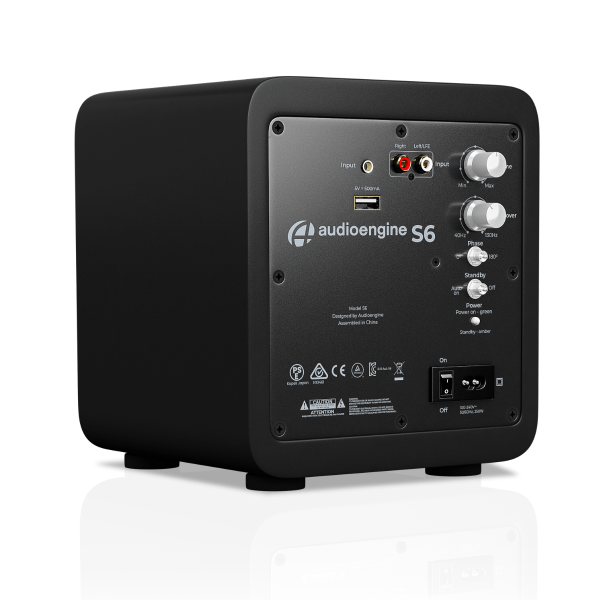
And since I’d purchased the wireless variant of the P6, Audiosource had also bundled its W3 wireless transmitter and receiver kit with the subwoofer:


The Sys left and right outputs both get split, with each output then routing in parallel both to the relevant Rekkr and to the W3 transmitter input’s correct channel. The receiver is roughly 12 feet away, to my left at the end of the room and connected to (and powered by) the back panel of the W6 subwoofer.
The transmitter and receiver aren’t even close to being line-of-sight aligned with each other, but the 2.4 GHz ISM band link between them still does a near-perfect job of managing connectivity. The only time I encounter dropouts, and then only briefly, is when a water-rich object (i.e., one of the humans, or our dog) moves in-between them. And although I was initially worried that the active W3 transmissions might destructively interfere with Bluetooth and/or Wi-Fi, I’m happy to report I haven’t experienced any degradation here, either.
Audio source diversityThat covers one end of the chain: now, what about the non-computer audio sources? There’s only one device, actually, shared between the two stacks, although its functional flexibility enables both native and connected content source diversity. And you’ve already heard about it, too; it’s the Bluesound NODE N130 that I initially mentioned at the beginning of 2023:


It integrates support for a diversity of streaming music services; although I could alternatively “tune in” to this same content via a connected computer, it’s nice not to have to bother booting one up if all I want to do is relax and audition some tunes. Integrated Bluetooth connectivity mates it easily with my Audio-Technica AT-LP60XBT turntable:

And a wiring harness mates it with the analog audio output of my ancient large-screen LCD computer monitor, acting as a pseudo TV in combination with my Xbox 360 (implementing Media Center Extender functionality) and Google Chromecast with Google TV.

The Bluesound NODE N130 has three audio output options, which conveniently operate concurrently: analog and both optical and coaxial (RCA) S/PDIF. The first goes to my Yamaha SR-C20A sound bar, the successor to the ill-fated Hisense unit I groused about back in mid-2023:

And the other two route to the Drop + Grace Design Standard DAC Balanced at the bottom of the left-side stack (optical S/PDIF):


and the Schiit Modi Multibit 1 DAC at the bottom of the right-side stack (coaxial RCA S/PDIF):


The multi-stack connectivity repetition is somewhat superfluous, but since it was a feasible possibility, I figured, why not? That said, I can always redirect one of the stack’s DACs to some other digitally tethered to-be-acquired widget in the future. And as mentioned in part 1 of this series, the Modi Multibit 1’s other (optical) S/PDIF input remains unpopulated right now, too.
That’s all (at least for now), folksAfter a two-post series spanning 2,000+ words, there’s my combo home office and “man cave” audio setup in (much more than) a nutshell. Feedback is, as always, welcomed in the comments!
—Brian Dipert is the Principal at Sierra Media and a former technical editor at EDN Magazine, where he still regularly contributes as a freelancer.
Related Content
- Sonic excellence: Music (and other audio sources) in the office, part 1
- Audio amplifiers: How much power (and at what tradeoffs) is really required?
- Audio Amplifiers from Class A, B, D to T
- Class D audio power amplifiers: Adding punch to your sound design
- Audio amplifier selection in hearable designs
- The Schiit Modi Multibit: A little wiggling ensures this DAC won’t quit
The post Sonic excellence: Music (and other audio sources) in the office, part 2 appeared first on EDN.
Сторінки


![[link]](https://i.redd.it/jihak2hc9pdg1.jpeg)