
Збирач потоків
Dell Technologies’ 2026 Predictions: AI Acceleration, Sovereign AI & Governance
Dell Technologies hosted its Predictions: 2026 & Beyond briefing for the Asia Pacific Japan & Greater China (APJC) media, where the company’s Global Chief Technology Officer & Chief AI Officer, John Roese, and APJC President, Peter Marrs, outlined the transformative technology trends and Dell’s strategies for accelerating AI adoption and innovation in the region.
 John Roese’s vision on the trends set to shape the technology industry in 2026 and beyond (Image Credits: Dell Technologies)
According to Roese, the rapid acceleration of AI is set to profoundly reengineer the entire fabric of enterprise and industry, driving new ways of operating, building, and innovating at an unprecedented scale and pace.
Focus on scalability and real adoption
A key trend is the shift in focus towards scaling AI for tangible business outcomes. “Conversations are on very real adoption, and AI is creating a truly transformational opportunity,” said Marrs. “We are working with customers across the region to build AI at scale.”
Marrs noted that growing deployment of agentic AI is an example of this transformation, with organizations such as Zoho in India already working with Dell to accelerate agentic AI adoption by delivering contextual, privacy-first and multimodal enterprise AI solutions. “AI has become more accessible for all companies in the region, and what we’ve been doing is successfully building foundations with customers to deploy AI at scale.”
Roese highlighted that the industry is now entering the autonomous agent era, where agentic AI is evolving from a helpful assistant to an integral manager of complex, long-running processes. “We expect that as people go on the agentic journey into 2026, they will be surprised by how much more agents do for them than they anticipated. Its very presence will bring value to make humans more efficient, and make the non-AI work, work better,” he noted.
As the industry continues to build and deploy more enterprise AI, Roese also emphasized the need for businesses to rethink how they treat and make resilient AI factories.
Sovereign AI and governance as the foundation for innovation
With the light-speed acceleration of AI development, there is a degree of volatility. Roese predicted that the demand for robust governance frameworks and private, controlled AI environments will become undeniable, urging the industry to build on both internal and external AI guardrails that allow organizations to innovate safely and sustainably.
“Last year, we predicted that ‘Agentic’ would be the word of 2025. This year, the word ‘Governance’ is going to play a much bigger role,” Roese said. “The technology and its use cases are not going to be successful if you do not have discipline and governance around how you operate your AI strategy as either an enterprise, a region, or a country.”
At national levels, the rapid rise of sovereign AI ecosystems will continue as AI becomes critical to state-level interests. Marrs discussed this trend’s momentum, noting that like many countries in the region, enterprises are also actively building their own frameworks to drive local innovation, with strong foundations already in place.
Building the ecosystem for impact and progress
To bridge that gap, Marrs reiterated the importance of a collaborative ecosystem in nurturing a skilled talent pool and advancing the region’s AI competitiveness, citing the APJ AI Innovation Hub as an initiative that is delivering impact through the combination of Dell’s capabilities, talent, and ecosystem.
“By working with experts, government, and industry peers, we’ve made unbelievable headway in fostering skill development and advancing our collective expertise,” said Marrs. “Together, we are accelerating Asia’s leadership as an AI region, identifying key steps to bolster the region’s growth. Dell is excited about how we’re participating and helping with this transformation.”
The post Dell Technologies’ 2026 Predictions: AI Acceleration, Sovereign AI & Governance appeared first on ELE Times.
NAL-CSIR Advances Field testing of Indigenous Defence Tech
The Council of Scientific and Industrial Research (CSIR)-National Aerospace Laboratories (NAL), in collaboration with Solar Defence & Aerospace Ltd. (SDAL), a private industry partner co-developed a 150-kg class Loitering Munition UAV (LM-UAV).
The drone system has an indigenous Wankel engine which is a perfect blend of efficiency and reliability, essential for defence products. With an operational range of up to 900 kilometres and an endurance for 6-9 hours, the drone is reliable for long missions. The system also has an operability at service ceilings reaching 5 kilometres which ensures altitude flexibility. The system is fitted with cutting edge features, such as GPS-denied navigation, essential for situations where the GPS is compromised, along with a low-radar cross-section that enhances its stealth characteristics.
The drone system is also updated with latest AI technology for target identification which will boost precision and autonomy during missions.
Next, is the field testing for High Altitude Platforms (HAPs), a solar-powered unmanned aircraft, capable of a sustained flight above a 20-kilometre altitude. These HAPs act as pseudo-satellites, used for extended surveillance, communication, and reconnaissance purposes.
The field testing of the 150-kg class LM-UAV and the development of solar-powered HAPs mark important milestones in India’s evolving indigenous defence technology landscape. These advancements are testament to the country’s commitment to building resilient and self-sustaining defence assets through collaborative public-private partnerships and cutting-edge aerospace research.
They are part of India’s efforts to develop self-reliant defence technologies under the ‘Atmanirbhar Bharat’ Initiative.
The post NAL-CSIR Advances Field testing of Indigenous Defence Tech appeared first on ELE Times.
Hardware security to bolster interconnect IPs for SoCs, chiplets

Hardware security vulnerabilities have greatly expanded the attack surface beyond traditional software exploits, making hardware security assurance crucial in modern system-on-chip (SoC) designs. Chip interconnect specialist Arteris’ acquisition of semiconductor cybersecurity assurance supplier Cycuity is the latest reminder of how hardware security is becoming an inflection point in SoC design.
Arteris delivers data-movement IP hardware and IP block integration software to connect on-chip components and chiplets. On the other hand, Cycuity ensures the security of these semiconductor design building blocks and their interactions. Charles Janac, president and CEO of Arteris, claims that Cycuity’s technology and expertise will add to Arteris’ product portfolio, enabling chip designers to better understand and improve data movement security in chiplets and SoCs.

Figure 1 A security solution, built around a coverage metric tailored for hardware designs, enables chip designers to precisely measure the effectiveness of security protocols. Cycuity
Cycuity’s hardware security solutions prevent vulnerabilities throughout chip development—from IP blocks to RTL design to full systems—with systematic security assurance in software configuration via scalable, repeatable security verification. The San Jose, California-based firm specifies, integrates, and verifies security across a chip’s hardware development lifecycle.
Security is becoming critical to all types of chip designs because the attack potential has expanded to the hardware layer. As a result, silicon vulnerabilities can compromise electronic systems and expose unprotected information. The National Institute of Standards and Technology (NIST) has recently released data showing common vulnerabilities and exposures (CVEs) in hardware grew by more than 15 times over the last five years.
For Arteris’ network-on-chip (NoC) IPs, which provide the backbone for data movement across SoCs and chiplets, Cycuity’s offerings can help mitigate security vulnerabilities throughout the SoC hardware development cycle. They can uncover security weaknesses across firmware, IP blocks, chip subsystems, chiplets, and full SoCs.

Figure 2 This hardware security solution identifies secure design assets and ensures they are properly managed during secure boot. Source: Cycuity
Cycuity—which works closely with leading EDA toolmakers such as Cadence, Siemens EDA, and Synopsys—has its hardware security tools integrated with leading EDA environments. That allows chip designers to identify, verify, and resolve security risks before silicon implementation and production. For instance, they can safeguard against attacks exploiting microarchitectural side channels, logic bugs, third-party and open-source IP, unsecured interconnects, debug backdoors, and supply-chain gaps.
The acquisition deal, subject to regulatory approval, is expected to close in the first quarter of 2026.
Related Content
- Interconnect: Switzerland of IP
- Closing Knowledge Gap on Hardware Security
- Why Hardware Security is the Preferred Choice for IIoT
- How physically aware interconnect IP bolsters SoC design
- Network-on-chip (NoC) interconnect topologies explained
The post Hardware security to bolster interconnect IPs for SoCs, chiplets appeared first on EDN.
Toyota & NISE Test Mirai Hydrogen FCEV in India Conditions
Toyota Kirloskar Motor (TKM) and the National Institute of Solar Energy (NISE) under the Ministry of New and Renewable Energy signed an MoU to collaborate to test Toyota’s Mirai, a hydrogen fuel-celled EV in Indian conditions.
The MoU was signed in the presence of Union Minister of New and Renewable Energy and Consumer Affairs, Food and Public Distribution, Prahlad Joshi in New Delhi. Under the said agreement, Toyota has handed over its Toyota Mirai to NISE who will conduct a comprehensive real-world test on the vehicle. The study will judge Mirai’s performance across Indian climates, terrains, and driving conditions.
NISE will study the fuel efficiency, real-world range, refuelling patterns, drivability, environmental resilience, along with the overall adaptability of the vehicle to Indian roads and traffic conditions. These results are then expected to manoeuvre the early-stage adoption of hydrogen mobility technologies in the country.
This initiative will be a breakthrough in the advancement for Hydrogen mobility in the country. It will also support India’s Green Hydrogen Mission and strengthen the country’s decarbonisation and clean transportation goals.
India’s decarbonization goals revolve around its Panchamrit targets: reaching 500 GW non-fossil fuel capacity and 50% renewable energy by 2030, cutting emissions intensity by 45% (vs. 2005) and reducing total emissions by 1 billion tonnes by 2030, all leading to Net-Zero by 2070, driven by massive solar, wind, green hydrogen, battery storage, and grid improvements.
The post Toyota & NISE Test Mirai Hydrogen FCEV in India Conditions appeared first on ELE Times.
Advanced Energy unveils dual-output 400W module for NeoPower configurable power supplies
Just got an oscilloscope 😎 looking at composite video signals
 | Nothing I'm just excited [link] [comments] |
Navitas expands global distribution network with Avnet
Nissan Powering EV Component Plant with Repurposed Batteries
Nissan Australia has launched the Nissan Node project, a circular economy initiative which will repurpose end-of-life Nissan Leaf batteries to power a section of its Dandenong production facility.
This initiative is part of Nissan’s sustainability strategy. The project involves the installation of a new solar array along with a battery-energy storage system, made from repurposed first-generation Leaf batteries at the Nissan Casting Australia Plant (NCAP).
EV manufacturing is said to have a 50-100% higher production emission as compared to ICE vehicles due to battery manufacturing.
Nissan expects its new system to cut NCAP’s annual CO2 emissions by nearly 259 tonnes while saving approximately 128 megawatt-hours of energy annually.
“This isn’t just a hugely exciting project, but an important step into the future for end-of-life EV batteries,” Nissan Oceania managing director Andrew Humberstone says.
“As an early pioneer of the electric vehicle both globally and locally, we can also demonstrate leadership in second-life battery initiatives. I’m proud that this solution is every bit as innovative as the launch of not only the Leaf but the recently introduced ARIYA.”
The initiative was delivered in partnership with Melbourne-based technology firm Relectrify, which developed the battery-management and inverter technology enabling second-life Leaf batteries to be repurposed effectively. Its ReVolve energy-storage system installed at NCAP is the first commercial product built entirely from retired Leaf batteries.
The post Nissan Powering EV Component Plant with Repurposed Batteries appeared first on ELE Times.
KEC, Powernet & Wise Integration Co-Develop AI Server SMPS Power Solutions
Wise Integration (France), Powernet (Korea) and KEC (Korea) will co-develop next-generation switched-mode power supply (SMPS) solutions designed specifically for AI server applications in South Korea. The partnership aligns with the country’s push to expand AI infrastructure and build out the next generation of high-density data centers.
Under the agreement, Wise Integration will supply its GaN (gallium-nitride) power devices, digital-control expertise and technical support. Powernet Technologies Corporation will lead development of new SMPS designs using Wise’s WiseGan and WiseWare technologies. KEC Corporation will manage backend manufacturing, including module integration and system-in-package production tailored to the thermal and reliability demands of AI-server racks.
In addition to accelerating the design and development of competitive AI-server power supply solutions and creating business opportunities in Korea’s AI server market, the project aims to shorten the solutions’ time-to-market using WiseGan and WiseWare technologies. The collaboration builds on an earlier partnership between Wise Integration and Powernet, launched to serve OEMs that require compact, digitally controlled power-supply systems for faster, smaller and more energy-efficient electronic equipment.
AI servers draw extensive power, generate intense heat, and depend on SMPS designs capable of converting high-voltage input (e.g., 400 V) to stable 48 V rails with minimal loss. GaN devices with digital control are uniquely suited for that task: they enable higher switching frequencies, greater efficiency, and more precise management of fast, high-current load transients.
Supporting South Korea’s National Ambition
The South Korean government’s investments in AI-dedicated data centers includes high-performance GPU clusters and digital infrastructure that supports demand for more efficient, compact, and scalable power-conversion systems.
“Korea is moving quickly to build the next generation of AI data centers, and power architecture is a critical piece of that effort. Working with Powernet and KEC lets us bring GaN-based digital control into server-grade designs at scale—delivering the efficiency, thermal performance, and responsiveness that modern AI hardware depends on,” said Ghislain Kaiser, CEO of Wise Integration.
Technology Momentum: A Logical Extension of Wise Integration’s Roadmap
Beyond the MoU, Wise Integration has been widening the foundation that supports strategic partnerships. As Korea accelerates AI-ready data-center development, the demands on power-conversion systems intensify—higher switching frequencies, tighter thermal budgets and more aggressive efficiency targets. Wise has been expanding its GaN + digital-control portfolio to meet those constraints, ensuring the technologies Korea aims to deploy at scale already have a maturing, production-validated base behind them.
For example, the company recently launched WiseWare 1.0 for totem-pole PFC and LLC topologies, its newest fully digital controller. While aimed today at gaming, displays and industrial systems, it shares the same architecture—high-frequency GaN operation, compact form factor, digitally managed efficiency—that naturally scales into the server-class designs targeted under the Korea-focused collaboration.
The post KEC, Powernet & Wise Integration Co-Develop AI Server SMPS Power Solutions appeared first on ELE Times.
FAMES Pilot Line R&D Advances: 400°C CMOS Enables 3D Integration Goals
CEA-Leti, the coordinator of the FAMES Pilot line, has achieved a major milestone for next-generation chip stacking: fully functional 2.5 V SOI CMOS devices fabricated at 400°C. The devices match electrical performance of devices fabricated at standard thermal budget (>1000 °C), removing one of the last barriers to large-scale 3D sequential integration (3DSI) —a core objective of FAMES.
Enabled by advanced CEA-Leti expertise in low-temperature processes (nanosecond laser annealing (NLA) and solid-phase epitaxy regrowth (SPER)), this work offers true three-dimensional device stacking from the lab to fab. 3D sequential-integration interconnection density between tiers is the highest among 3D technologies, such as TSV and hybrid bonding. In this project, CEA-Leti demonstrated that Si CMOS is BEOL compatible, and thus can be stacked safely above BEOL, while transistor performance and maturity overtake largely the other technological options from the state-of-the-art, low-temperature solutions.
The achievement, presented today in a paper at IEDM 2025, titled, “High Performance 2.5 V n&p 400 °C SOI MOSFETs: A Breakthrough for Versatile 3D Sequential Integration,” is a key breakthrough for the FAMES Pilot Line, a European Union initiative launched in 2023 in response to the EU Chips Act strategy to strengthen sovereignty and competitiveness in semiconductor technologies. By combining 3D heterogeneous and sequential integration on FD-SOI platforms, the consortium aims to enable a new generation of More-Than-Moore devices and applications.
Enabling New Chip Architectures
“This breakthrough is a major milestone of the FAMES project as it enables innovative new chip architectures,” said Dominique Noguet, CEA-Leti vice president and coordinator of the FAMES Pilot Line. “Our low-temperature process could accelerate real-world demonstrations of multi-tier stacks combining advanced CMOS logic, with smart pixel or RF layers, to create new high-performance 3D chips.”
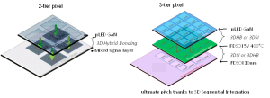 Concept of 3-tier µLED GaN pixel allowing an emissive array with strong pitch reduction thanks to 3DSI in combination with 3D hybrid bonding technology. CEA-Leti’s 400 °C CMOS process enables such top-tier integration without exceeding the thermal limits of the active circuitry below.
The team showed that SOI devices processed at 400 °C instead of the high temperature (>1000 °C) industry standard and high-temperature industrial reference, performed equivalent to high-temperature devices.
“The 400 °C process enables 3D sequential stacking on any bottom tier,” Noguet said. “It’s a huge step forward because it’s far more mature—reliable and scalable—than current low-temperature solutions, such as polycrystalline films, oxide semiconductors or carbon nanotubes.”
Protecting Circuitry on Bottom-Tier LayersCEA-Leti’s team demonstrated n- and p-type transistors matching the characteristics of conventional high-temperature CMOS devices, while staying within the ≤400 °C thermal budget required to preserve active circuitry in lower layers.
The process relies on an optimized 400 °C LPCVD deposition for amorphous silicon followed by NLA in the melt regime for dopant activation and diffusion—producing polycrystalline, low-resistance gates with excellent interface quality. In addition, NLA-SPER mastering enables dopant activation without diffusion leading to access resistance within specifications.
The post FAMES Pilot Line R&D Advances: 400°C CMOS Enables 3D Integration Goals appeared first on ELE Times.
Keysight & KT SAT Nail Industry First GEO-to-LEO Multi-Orbit NTN Handover!
Keysight Technologies, Inc., in collaboration with KT SAT, has demonstrated a successful non-terrestrial network (NTN) handover using the KOREASAT-6A satellite at KT SAT’s Kumsan Satellite Network Operation Center in Korea. In a controlled clinical environment, the companies established the industry’s first NR-NTN multi-orbit handover between a commercial GEO satellite and an emulated LEO link. The demonstration was performed over a live Ku‑band GEO connection (DL ~12.3 GHz / UL ~14.4 GHz), marking a major milestone toward testing the newly standardized 3GPP Rel‑19 Ku‑band NTN spectrum. By incorporating Ku‑band operation into this multi-orbit mobility scenario, Keysight and KT SAT have validated NTN behaviors in a frequency range now central to emerging global standards and operator deployment strategies.
As the industry moves toward 6G, integrating satellite and terrestrial networks is essential to deliver continuous coverage and resilient service in remote or disaster-affected areas. Satellite links, however, introduce longer delays, Doppler effects, and dynamic link conditions that complicate mobility and handover across space and ground domains.
By moving beyond earlier demonstrations focused on single-orbit GEO connectivity, KT SAT and Keysight have shown how operators can evolve from point-to-point satellite links to continuous multi-orbit mobility, expanding KT SAT’s service capabilities toward resilient, always-on coverage across space and ground domains. This achievement also establishes an important technical milestone for KT SAT and Keysight in advancing Ku-band NTN mobility.
Using Keysight’s Network Emulator Solutions and UeSIM RAN Testing Toolset, the teams emulated the base station and user equipment, established a two-way link through KOREASAT-6A, and maintained service continuity during a handover from GEO to an emulated LEO connection. Operating the GEO link in Ku‑band ensures that these mobility insights directly map to the Rel‑19 NTN frequency bands now entering commercial planning, giving operators and device vendors earlier visibility into real‑world propagation, timing, and interoperability behaviors. As a result, KT SAT can now explore and validate advanced NTN mobility scenarios in the lab, before satellites or user devices are widely deployed, accelerating its roadmap and reducing the time and cost of bringing new multi-orbit services to market.
This collaboration shows how operators can extend coverage and resilience, while device and chipset vendors gain a lab-based path to validate NTN mobility without relying solely on expensive field trials. Insights from this work are intended to inform standards discussions and operator evaluations, helping the ecosystem shorten time-to-trial and de-risk commercialization.
Seo Young-soo, CEO of KT SAT, said: “As the only satellite communications service provider in Korea, KT SAT is progressively validating the applicability of NTN gNB and UE using our five operational GEO satellites. Building on the results of this trial, we will actively explore strengthening the competitiveness of our next-generation GEO satellite for the global market and delivering integrated multi-orbit communication services based on NTN systems, including traffic handover across our own GEO and future LEO/MEO constellations.”
Peng Cao, Vice President and General Manager of Keysight’s Wireless Test Group, Keysight, said: “This demonstration shows how emulation can bring future multi-orbit networks into the lab today. By combining a live GEO connection with emulated LEO conditions using NR-NTN parameters in Ku-band, Keysight gives operators and vendors a practical way to study NTN handover behavior, optimize mobility strategies, and reduce the cost and risk of early deployments.”
The post Keysight & KT SAT Nail Industry First GEO-to-LEO Multi-Orbit NTN Handover! appeared first on ELE Times.
This A very powerful Amplifier module runs at 12v Dc
 | It can deliver upto 12.5 watts (across both the channels) when it is powered with 16v Dc.Means it can run two speaker on 6.25watts (6.25 × 2). [link] [comments] |
DIY Film Capacitor 27.5nF
 | I made this film capacitor yesterday with 2 ~4m nickel strips I had laying around (0.1mm x 11mm) with kapton tape as the dielectric. I wrapped it around a screw to form the shape and wrapped electrical tape around the outermost coil. Then I hot glued the uncovered coils to keep everything in place. I took the screw out and filled the void left behind with hot glue. The capacitor now measures around 27.5nF. I've been having trouble measuring held voltage with a DMM and oscilloscope. I think that's due to the inherent load the voltmeter and oscilloscope add. Nonetheless, my TC1 and my Kaiweets DMM both calculate around the same capacitance. This isn't really useful to me, but the nickel strip I had lying around was even less so, so I think this is a cool trinket. [link] [comments] |
Low-power Wi-Fi 6 MCUs preserve IoT battery life

Renesas has announced the RA6W1 dual-band Wi-Fi 6 wireless MCU, to be followed by the RA6W2 Wi-Fi 6 and BLE combo MCU. Based on an Arm Cortex-M33 CPU running at 160 MHz, these low-power microcontrollers dynamically switch between 2.4-GHz and 5-GHz bands in real time, ensuring a stable, high-speed connection.

The RA6W1 and RA6W2 MCUs use Target Wake Time (TWT) to let IoT devices sleep longer, extending battery life and reducing network congestion. They consume as little as 200 nA to 4 µA in deep sleep and under 50 µA while checking for data, enabling devices to stay connected for a year or more on a single battery. This makes them well-suited for applications requiring real-time control, remote diagnostics, and over-the-air updates— for example, environmental sensors, smart home devices, and medical monitors.
Alongside the RA6W1 and RA6W2 MCUs, Renesas launched two fully integrated modules designed to reduce development time and accelerate time to market. The Wi-Fi 6 (RRQ61001) and Wi-Fi 6/BLE combo (RRQ61051) modules feature built-in antennas, certified RF components, and wireless protocol stacks that comply with global network standards.
The RA6W1 MCU in WLCSP and FCQFN packages, as well as the RRQ61001 and RRQ61051 modules, are available now. The RA6W2 MCU in a BGA package is scheduled for release in Q1 2026.
The post Low-power Wi-Fi 6 MCUs preserve IoT battery life appeared first on EDN.
Automotive buck converter is I2C-tuned

Optimized for automotive point-of-load (POL) applications, Diodes’s AP61406Q 5.5-V, 4-A synchronous buck converter provides a versatile I2C programming interface. The I2C 3.0-compatible serial interface supports SCL clock rates up to 3.4 MHz and allows configuration of PFM/PWM modes, switching frequencies (1 MHz, 1.5 MHz, 2 MHz, or 2.5 MHz), and output-current limits of 1A, 2 A, 3 A, and 4 A. The output voltage is adjustable in 20-mV increments.

The AP61406Q uses a proprietary gate-driver scheme to suppress switching-node ringing without slowing MOSFET transitions, helping reduce high-frequency radiated EMI. It operates from an input of 2.3 V to 5.5 V and integrates 75-mΩ high-side and 33-mΩ low-side MOSFETs for efficient step-down conversion. Constant on-time (COT) control further minimizes external components, eases loop stabilization, and delivers low output-voltage ripple.
Offered in a W-QFN1520-8/SWP (Type UX) package, the converter is AEC-Q100 qualified for operation from –40°C to +125°C. Its protection suite—including high-side and low-side current-sense protection, UVLO, VIN OVP, peak and valley current limiting, and thermal shutdown—enhances reliability.
The post Automotive buck converter is I2C-tuned appeared first on EDN.
SiC power modules deliver up to 608 A

SemiQ continues to expand its Gen3 QSiC MOSFET portfolio with 1200-V power modules offering high current density and low thermal resistance. The new seven-device lineup includes high-current S3 half-bridge, B2T1 six-pack, and B3 full-bridge modules designed to meet the needs of EV chargers, energy storage systems, and industrial motor drives.

Two of the devices handle currents up to 608 A with a junction-to-case thermal resistance of just 0.07 °C/W in a 62‑mm S3 half-bridge format. The three six-pack modules integrate a three-phase power stage into a compact housing, offering on-resistance from 19.5 mΩ to 82 mΩ, an optimized layout, and minimal parasitic effects. The two full-bridge modules combine current handling up to 120 A with on-resistance as low as 8.6 mΩ and a thermal resistance of 0.28 °C/W.

All parts undergo wafer-level gate-oxide burn-in and are breakdown-tested above 1350 V. Gen3 modules operate at lower gate voltages (18 V/-4.5 V) and reduce both on-resistance and turn-off energy losses up to 30% versus previous generations.
The power modules are available immediately. Explore SemiQ’s entire line of Gen3 MOSFET power modules here.
The post SiC power modules deliver up to 608 A appeared first on EDN.
Handheld analyzers cut through dense RF traffic

With 120-MHz gap-free IQ streaming, Keysight’s N99xxD-Series FieldFox analyzers ensure every signal event is captured. This capability lets users stream and replay complex RF activity to quickly pinpoint issues and verify system performance. The result is deeper analysis and greater confidence that key signal details are not overlooked in the field.

The N99xxD-Series includes 14 handheld models—combo or spectrum analyzers—covering frequencies from 14 GHz to 54 GHz. Each model supports more than 25 software-defined FieldFox applications, including vector network analysis, spectrum and real-time spectrum analysis, noise figure measurement, EMI analysis, pulse signal generation, and direction-finding.
Key capabilities of the N99xxD-Series include:
- 120-MHz IQ streaming with SFP+ 10-GbE interfaces for uninterrupted data capture
- Wideband signal analysis and playback for troubleshooting, spectrum monitoring, and interference detection
- Field-to-lab workflow to recreate real-world signals for lab analysis
- High RF performance with ±0.1 dB amplitude accuracy without warm-up
A technical overview of Keysight’s FieldFox handheld analyzers and D-Series information can be found here.
The post Handheld analyzers cut through dense RF traffic appeared first on EDN.
MOSFETs bring 750-V capability to TOLL package

Now in mass production, Rohm’s SCT40xxDLL series of SiC MOSFETs in TOLL (TO-Leadless) packages delivers high power-handling capability in a compact, low-profile form factor. According to ROHM, the TOLL package provides roughly 39% better thermal performance than conventional TO-263-7L packages.

The SCT40xxDLL lineup consists of six devices, each rated for a 750-V maximum drain-source voltage, compared to the 650-V limit typical of standard TOLL packages. This higher voltage rating enables lower gate resistance and a larger safety margin for surge voltages, helping to further reduce switching losses.

In AI servers and compact PV inverters, rising power requirements coincide with pressure to reduce system size, increasing the need for higher-density MOSFETs. In slim totem-pole PFC designs with thickness limits near 4 mm, Rohm’s new devices cut footprint to 11.68×9.9 mm (about 26% smaller) and reduce package height to 2.3 mm, about half that of typical devices.
The 750-V SiC MOSFETs are available from distributors such as DigiKey, Mouser, and Farnell. For details and datasheets, click here.
The post MOSFETs bring 750-V capability to TOLL package appeared first on EDN.
Wise Integration, Powernet and KEC sign MoU to co-develop SMPS solutions for AI server power supplies in Korea
Splitting voltage with purpose: A guide to precision voltage dividers

Voltage division is not just about ratios; it’s about control, clarity, and purpose. This little guide explores precision voltage dividers with quiet confidence, and sheds light on how they shape signal levels, reference points, and measurement accuracy.
A precision voltage divider produces a specific fraction of its input voltage using carefully matched resistive components. It’s designed for accurate, stable voltage scaling—often used to shape signal levels, generate reference voltages, or condition inputs for measurement. Built with low-tolerance resistors, these dividers ensure consistent performance across temperature and time, making them essential in analog design, instrumentation, and sensor interfacing (Figure 1).

Figure 1 Representation of an SOT23 precision resistor-divider illustrates two tightly matched resistors with accessible terminals at both ends and the midpoint. Source: Author
A side note: While the term precision voltage divider broadly refers to any resistor-based circuit that scales voltage, precision resistor-divider typically denotes a tightly matched resistor pair in a single package, for example, SOT23. These integrated devices offer superior ratio accuracy and thermal tracking, making them ideal for reference scaling and threshold setting in precision analog designs.
As an unbiased real-world example, the HVDP08 series from KOA is a thin-film resistor network designed for high-precision, high-voltage divider applications. It supports resistance values up to 51 MΩ, working voltages up to 1,000 V, and resistance ratios as high as 1000:1.

Figure 2 The HVDP08 high-precision, high-voltage divider achieves higher integration while reducing board space requirements and overall assembly overhead. Source: KOA
Similarly, precision decade voltage dividers—specifically engineered for use as input voltage dividers in multimeters and other range-switching instruments—are now widely available. Simply put, precision decade voltage dividers are resistor networks that provide accurate, selectable voltage ratios in powers of ten. One notable example is the EBG Series 1776-X, widely recognized for its precision and reliability.

Figure 3 EBG Series 1776-X precision decade resistors incorporate ceramic protection and laser-trimmed thin films to achieve ultra-tight tolerances. Source: Miba
Moreover, digitally programmable precision voltage dividers—such as the MAX5420 and MAX5421—are optimized for use in digitally controlled gain amplifier configurations. Programmable gain amplifiers (PGAs) allow precise, software-driven control of signal amplification, making them ideal for applications that require dynamic range adjustment, calibration, or sensor interfacing.
Poorman’s precision practice
Precision does not have to be pricey. In this section, we explore how resourceful design choices—clever resistor selection, thoughtful layout, and a dash of calibration—can yield surprisingly accurate voltage dividers without premium components. Whether you are prototyping on a budget or refining a DIY instrument, this hands-on approach proves that precision is within reach.
Achieving precision on a budget starts with clever resistor selection: Choosing resistors with tight tolerances, low temperature coefficients, and stable long-term behavior, even if they are not top-shelf brands. A thoughtful layout ensures minimal parasitic effects; short traces, good grounding, and avoiding thermal gradients all help preserve accuracy. Finally, a dash of calibration—whether through trimming, software correction, or referencing known voltages—can compensate for small mismatches and elevate a humble design into a reliable performer.
While selecting resistors, it’s important to distinguish between absolute and relative tolerance. Absolute tolerance refers to how closely each resistor matches its nominal value, say ±1% of 10 KΩ. Relative tolerance, on the other hand, describes how well matched a pair or group of resistors are to each other, regardless of their deviation from nominal. In voltage dividers, especially precision ones, relative tolerance often matters more. Even if both resistors drift slightly, as long as they drift together, the ratio—and thus the output voltage—remains stable.
As an aside, ratio tolerance refers to how closely a resistor pair maintains its intended resistance ratio, independent of their absolute values. In precision voltage dividers, this metric is key; even if both resistors drift slightly, a tight ratio tolerance ensures the output voltage remains stable. It’s a subtle but critical factor when accuracy depends more on matching than on nominal values.
Having covered the essentials, we now turn to a hands-on example, one that puts theory into practice with accessible components and practical constraints.
Operational amplifier (op-amp) circuits are commonly used to scale the output voltage of digital-to-analog converters (DACs). Two popular configurations—the non-inverting amplifier and the inverting amplifier—can both amplify the signal and adjust its DC offset.
For applications requiring output scaling without offset, the goal is to expand the voltage range of the DAC’s output while maintaining its original polarity. This setup requires the op-amp’s positive supply rail to exceed the desired maximum output voltage.

Figure 4 This output-scaling circuit extends DAC’s voltage range without altering its polarity. Source: Author
Output voltage formula: VOUT = VIN (1 + RF/RG)
Scaling in action
To scale a DAC output from 0–5 V to 0–10 V, a gain of 2.0 is required.
Using a 10K feedback resistor (RF) and a 10K gain resistor (RG), the gain becomes 2. This configuration doubles the DAC’s output voltage while preserving its zero-based reference.
You can also design op-amp circuits to scale and shift the DAC output by a specific DC offset. This is especially useful when converting a unipolar output, for example, 0 V to 2.5 V, into a bipolar range, for instance, –5 V to +5 V. But that’s a story for another day.
Precision voltage dividers may seem straightforward, but their influence on signal integrity and measurement accuracy runs deep. Whether you are working on analog front-ends, reference rails, or sensor inputs, careful resistor selection and layout choices can make or break performance.
Have a go-to divider trick or layout insight? Drop it in the comments and join the conversation.
 T. K. Hareendran is a self-taught electronics enthusiast with a strong passion for innovative circuit design and hands-on technology. He develops both experimental and practical electronic projects, documenting and sharing his work to support fellow tinkerers and learners. Beyond the workbench, he dedicates time to technical writing and hardware evaluations to contribute meaningfully to the maker community.
Related Content
- Resistive voltage dividers
- Voltage and Current Divider
- Designing precision analog front ends
- Introduction to Voltage Divider Basic and Rules
- Achieving analog precision via components and design, or just trim and go
The post Splitting voltage with purpose: A guide to precision voltage dividers appeared first on EDN.
Сторінки


![[link]](https://i.redd.it/kjc8idqg7n6g1.jpeg)