
Збирач потоків
Cadence Adds Digital Twin for Nvidia’s AI Data Center Compute Platform
Київська політехніка продовжує розвивати космічну програму!

Голова Наглядової ради КПІ ім.
Stamp Turns Messy Breadboards Into Swappable PCB Blocks
Перше засідання оновленого складу Наглядової ради

Нещодавно відбулося перше засідання оновленого складу Наглядової ради КПІ ім. Ігоря Сікорського, присвячене розвитку та особливостям функціонування університету в період воєнного стану.
Fake contacts, bounced to order

Many recent Design Ideas have involved button-pushing to control power. Some may have been more resistant to contact-bounce than others—but how can we really check that? This DI describes how some simple circuitry can simulate bouncy contacts, and do so controllably and repeatably, thus allowing an objective measure of how well the debouncing works.
Wow the engineering world with your unique design: Design Ideas Submission Guide
Other solutions are available! Capturing the bounces from a real switch and then replaying them at varying rates is one approach, and SPICE models are apparently available. I’ve not played with the latter, but trust that its developers had fun simulating some truly evil conditions.
Genuine contact noise is inherently random and often very spiky. This device, shown in detail in Figure 1, uses bursts of well-defined pulses instead. If your debouncing circuitry or code can handle those, real-world operation is pretty much guaranteed. Because these pulses are grouped in bursts and are repeatable, the guard time can easily be measured. Hook this across the (normally-open) contacts whose debouncing you need to check, and vary the burst duration until your system misbehaves.
Push switches vary a lot, as some quick tests revealed. Clicky tact(ile) ones showed little or even no bounce when closing. A cheap doorbell push was, putting it politely, somewhat worse, though admittedly it was intended to switch a contact-cleaning amp or so. While most were noisier when opening than closing, they were generally stable within 20 ms (doorbell button excepted), so the span of 100 µs to 100 ms should be adequate for testing.
 Figure 1 This contact-bounce simulator generates brief bursts of pulses when the Run button is either pressed or released, the burst durations ranging from about 100 µs to 100 ms. The optocoupler provides an isolated output that can pull up or down as needed.
Until the Run button is pressed, oscillator U1a is inhibited and the circuit is static, so no power is drawn—nanoamp leakages excepted—and the output is open circuit. Pressing Run enables the oscillator. After a brief delay (C1/R2) to mask the initial clock edge, it also clears U2a’s reset, allowing U2a to count up to 8 and then freeze or dead-end itself. Pulses from its Q1 are indirectly fed to the optocoupler OCI1 to simulate the “making” bounces, followed by a steady level from Q4 once the switch is deemed to be properly closed. U2b is inactive during this sequence. Figure 2 shows the various waveforms.
What’s pushed down must come up
When Run is released, C2 and R3 ensure that the oscillator still operates for ~200 ms. U2a is reset, clearing the steady “on” condition and allowing U2b to count up while its Q1 delivers the “breaking” bounces. Finally, U2b freezes, and everything can turn off, ready for the next test cycle.
D2–4 and R6 OR the pulses and the steady level. The first attempt used a 74HC02 (quad NOR) to do that, but there were so many odd gates left over that it all just looked unhappy. Employing diode logic plus the spare U1 gates for buffering cured that.

Figure 2 A composite of waveforms from the circuit of Figure 1, with some notes on its operation.
This view of the waveforms exposes a slight hiccup! Note how the making and breaking sequences differ, with the latter starting at an arbitrary point on the clock, giving an extra pulse or part thereof. Adding more logic could have cured that by synchronizing U2a’s reset with the clock, but while more elegant ’scope-wise, it had no practical advantage. Anyway, as we saw above, many buttons are electrically noisier when their contacts are opening.
An easy way out, and a harder one
Now that we have the bursts, we need to make them look like actual switch closures. The simplest and generally best way is to drive them into the LED of an optocoupler, as shown in Figure 1. Its transistor is the output switch, which can pull up or down as required. Its effective resistance may be significant; an (obsolete) FCD820 driven with ~7 mA looked like ~500 Ω.
That’s fine for logic-level applications, but if more grunt is needed, MOSFETs are better because they conduct much harder. Figure 3 shows some add-on variants ranging from simple pull-down and pull-up/pull-down circuits—both non-isolated—to a fully isolated arrangement. Note the necessary power and ground feeds from the target. The devices shown are good for 60 V, a few ohms, and moderate currents.

Figure 3 MOSFETs can be used to switch the output with much less “contact resistance.” This shows three ways of doing that, with both isolated and non-isolated outputs.
Isolating the output with a reed relay is a non-starter. They take several milliseconds to respond, which is slower than we need, and chatter badly (mercury-wetted ones excepted). On a positive note, this gadget can easily simulate them, at least for simple makes or breaks: replace the Run button with a suitably-driven OCI.
A digression and a rant
Why do many single-function buttons refuse to do anything useful until they are released? With multi-function ones—perhaps intended to distinguish between short presses, long ones, and being inadvertently sat on—it makes good sense, but when there are no other options, it’s irrational. Once a switch has been seen as valid for long enough, it should be treated as such. I can’t be alone in having an almost instinctive reaction to delayed results: either “Ooh—there must be other options” or “Arggh—it’s broken”, neither of which is usually true or helpful.
Though I did accidentally find the (undocumented) subtitles’ control on the remote for my new TV by holding the mute button down for too long. According to said documentation, that function was inaccessibly buried—in the Accessibility Menu. Buttons often seem to be seen as trivial afterthoughts, but when they are part of a user interface, they need to be implemented (and debounced) with subtlety and care. And properly documented for the user. End of rant.
—Nick Cornford built his first crystal set at 10, and since then has designed professional audio equipment, many datacomm products, and technical security kit. He has at last retired. Mostly. Sort of.
Related Content
- To press on or hold off? This does both.
- Push ON, Push OFF for AC voltages
- A different twist to the power pushbutton problem: A kilowatt AC DAC
- Flip ON flop OFF
- Another simple flip ON flop OFF circuit
- Flip ON flop OFF without a flip/flop
- Elaborations of yet another Flip-On Flop-Off circuit
- Latching D-type CMOS power switch: A “Flip ON Flop OFF” alternative
- Another simple flip ON flop OFF circuit
- Latching power switch uses momentary pushbutton
The post Fake contacts, bounced to order appeared first on EDN.
The fundamentals of cadence sensing for pedal rotation tracking

A cadence sensor is a compact cycling device that measures your pedaling rate in revolutions per minute (RPM), providing real-time feedback to help optimize performance and training efficiency. Here is a hands-on guide to the core principles behind pedal rotation tracking, along with practical setup tips for bikes and DIY projects. It provides clear explanations and actionable insights to get your cadence sensor up and running with confidence.
Read the full article at EDN’s sister publication, Planet Analog.
Related Content
- High-performance Electric Bicycles
- The Basics of Torque Measurement
- Battery Innovations Power Electric Bike
- Motor Speed Control Using Hall-Effect Sensors
- World’s first Bluetooth low energy bike speed and cadence monitor is released
The post The fundamentals of cadence sensing for pedal rotation tracking appeared first on EDN.
💡 Today was a good day!
 | A client approached me because their system suddenly stopped working.The system was designed by someone else and had been working fine for years. After carefully studying the schematics, checking power supply, and measuring continuity with a multimeter, I spent hours debugging the issue. Replaced both. System came back to life. Minimal cost. Maximum satisfaction. 😊 [link] [comments] |
Why Electronics and Auto Manufacturers Struggle with Compliance in India
Electronics and automobile manufacturers, contributing 3% and 7.1% to India’s GDP respectively, are at the heart of the nation’s industrial growth. Yet, their progress is often slowed by a maze of compliance requirements from evolving labour codes and plant safety regulations to environmental certifications and state-specific laws. For many players, these overlapping obligations translate into delays, operational inefficiencies, and missed opportunities to scale.
To understand how compliance challenges are shaping the future of these sectors, and how technology like AI and RPA is redefining compliance management, ELE Times spoke with Munab Ali Beik, Head of Compliance Advisory at Core Integra. With over 20 years of experience navigating regulatory frameworks and driving digital compliance transformations, he provides deep insights into the hurdles manufacturers face, the reforms needed to unlock growth, and how smart compliance practices can strengthen India’s position as a global manufacturing hub.
Excerpts from the interview:
ELE Times: What are the most complex compliance requirements currently troubling electronics and automobile manufacturers in India?
Munab Ali Beik: For electronics and automobile manufacturers, the most complex compliance challenges today revolve around evolving labour laws, contractor & supplier compliances, shop floor regulations, health and safety requirements, unions and employee welfare norms. With the introduction of upcoming new labour codes, companies must realign HR policies, wage structures, obtaining registrations and working hours while maintaining strict adherence to health and safety standards. Shop floor compliance has become increasingly demanding, requiring detailed SOPs, audits, and documentation to manage risks associated with heavy machinery. Beyond this, manufacturers face intricate requirements around plant certifications, environmental regulations, product safety standards, certifications, audits and overall labour law compliance. Studies indicate that nearly 45–50% of players’ experience delays and operational inefficiencies due to these overlapping regulatory demands, highlighting the critical need for proactive compliance management.
ELE Times: Why do almost half of manufacturers experience delays specifically due to compliance hurdles?
Munab Ali Beik: The delay is due to compliance hurdles because the regulatory landscape remains highly complex and fragmented. Frequent updates to labour laws and enterprise laws require constant adjustments, while machinery safety norms and employee welfare provisions add operational challenges. For companies operating multiple plants, the lack of uniformity across states further complicates compliance, state-specific laws, local regulatory requirements, and varying environmental norms necessitate separate processes and documentation. States have indicated that the Ease of Doing Business initiative may complicate the procedural implementations and understanding the simplified part of compliances. This patchwork of regulations, combined with limited coordination across jurisdictions, creates bottlenecks and inefficiencies, slowing operations and impacting manufacturers’ ability to scale effectively.
ELE Times: With electronics contributing 3% and automobiles 7.1% to India’s GDP, do you think regulatory overload is limiting their full growth potential?
Munab Ali Beik: Yes, absolutely. If compliance hurdles were streamlined, electronics and automobile manufacturers could devote far more resources to R&D, innovation, and building global competitiveness. These sectors have the potential to not only sustain but significantly increase their contribution to India’s GDP by boosting exports, enhancing localization, and developing advanced manufacturing ecosystems. Procedural bottlenecks currently divert focus from scaling production, investing in cutting-edge technologies, and optimizing supply chains. While India is making strides in improving ease of doing business, attracting larger foreign investments and sustaining growth requires simpler and more stable compliance frameworks. The central and state governments are set to relax certain provisions for the electronics and automobile manufacturing sectors to improve their performance. These relaxations pertain to auto-renewals, inspections, self-certifications, working hours, overtime, industrial disputes, subsidies, and promotional activities. Reducing regulatory overload would enable these industries to strengthen core operations, accelerate India’s emergence as a global manufacturing hub, and unlock untapped economic potential.
ELE Times: How can AI and RPA truly transform compliance management for manufacturing plants?
Munab Ali Beik: AI and RPA can revolutionize compliance management in manufacturing by automating repetitive tasks like payroll, attendance tracking, statutory filings, registers maintenance, returns filing, maintaining the data, Management information system and audit reporting. AI platforms provide real-time visibility, flag risks, and update changes in regulations automatically, while RPA ensures consistent workflows across HR, finance, and operations. This reduces errors, boosts efficiency, and frees management to focus on strategic priorities. Over time, digital compliance not only cuts costs, increase the efficiency, error free and improves safety monitoring but also strengthens governance and investor confidence.
ELE Times: What critical changes are required to make India a global manufacturing hub for electronics and automobiles?
Munab Ali Beik: To position India as a global manufacturing hub for electronics and automobiles, critical changes are needed in regulatory stability, ease of doing business, exemption from regulatory frameworks and policy clarity. Simplifying access to government schemes, enhancing transparency in labour laws, and streamlining compliance processes will reduce operational friction and build investor confidence. These measures will enable manufacturers to focus on innovation, scale efficiently, and compete globally, driving both domestic growth and export potential.
ELE Times: How is Core Integra evolving its AI/RPA tools to stay aligned with future compliance expectations?
Munab Ali Beik: We are continuously enhancing our AI and RPA capabilities through our compliance platform, Ctrl F, to stay ahead of evolving regulatory requirements. We leverage AI to track changing laws in real time, identify the impacts, flag risks, and automate documentation, filings, and reporting. By integrating RPA, we ensure consistency across multi-location operations, reduce manual errors, simplified the process and minimize administrative burdens. Alongside technology, we invest in R&D and advisory expertise to simplify complex regulations and provide proactive compliance updates. These innovations empower our clients to manage compliance efficiently, enhance operational oversight, and focus resources on scaling and innovation.
The post Why Electronics and Auto Manufacturers Struggle with Compliance in India appeared first on ELE Times.
Unlocking the Power of AI: A Strategic Guide for OEMs and ISVs
Artificial intelligence is no longer some faraway notion; it has become a strong and immediate agent of innovation. Whether in predictive analytics or generative design, AI remains instrumental in the means by which OEMs and ISVs conceive, produce, and maintain their products. However, promising this technology is, majority of companies cannot speed away from experimentation into value-driven and large-scale application.
This guide demystifies the AI technologies reshaping the industry, illuminates their real-world applications, and lays down a commercially viable roadmap for OEMs and ISVs to embrace AI with confidence and clarity.
Understanding Artificial Intelligence
AI refers to the development of computer systems capable of performing tasks traditionally requiring human intelligence. These systems process vast amounts of data, recognize patterns, and make decisions with minimal human intervention. AI spans a wide spectrum from rule-based automation to advanced deep learning algorithms capable of generating content, interpreting speech, and predicting outcomes.
While AI has existed for decades, the surge in computational power, cloud infrastructure, and data availability has accelerated adoption across industries. Today, AI is no longer optional it is an essential enabler for companies striving to remain innovative and competitive.
The Different Types of AI:
Natural Language Processing (NLP)
NLP enables machines to understand, interpret, and generate human language. It powers chatbots, virtual assistants, translation tools, and sentiment analysis systems. OEMs and ISVs are integrating NLP into products to create voice-enabled interfaces, enhance customer engagement, and extract insights from unstructured data such as emails, reviews, and social media.
Machine Learning and Predictive Analytics
Machine Learning (ML) allows systems to learn patterns from data and make predictions without explicit programming. Predictive analytics, a major ML application, helps anticipate trends, detect anomalies, and optimize operations. For instance, predictive maintenance reduces downtime by forecasting equipment failures, while cybersecurity solutions use ML to detect threats in real-time.
Generative AI
Generative AI is the next frontier. Unlike traditional ML, it creates new content—ranging from text and images to design prototypes. For OEMs and ISVs, this translates into automated documentation, rapid product prototyping, and personalized customer experiences. Generative AI not only streamlines workflows but also fosters creativity and innovation.
Addressing the Challenges of AI Adoption:
Despite its potential, AI adoption comes with hurdles-
Bias and Fairness: AI models trained on biased datasets risk producing unfair or inaccurate outcomes. Businesses must prioritize transparency and accountability in AI systems.
Integration Complexity: Legacy infrastructure, siloed data, and fragmented workflows often complicate AI integration.
Data Security and Privacy: AI systems process sensitive business and customer information, making strong data governance and compliance with privacy regulations critical.
Continuous Adaptation: AI models require constant monitoring, retraining, and refinement to remain accurate in dynamic business environments.
Deploying AI Strategically for OEMs and ISVs:
To move beyond pilots and achieve scalable impact, businesses should approach AI strategically:
- Align AI with Business Goals – Identify specific areas where AI can enhance value, such as automation, customer engagement, or operational efficiency.
- Ensure Data Readiness – High-quality, structured data is the backbone of AI success. Companies must invest in robust data collection and management systems.
- Leverage Cloud and AI-as-a-Service – Cloud-based platforms lower barriers to entry by offering scalable AI tools without requiring deep in-house expertise.
- Collaborate with AI Experts – Partnering with specialized providers accelerates adoption and optimizes solutions for industry-specific needs.
- Commit to Continuous Improvement – Regularly monitor performance, retrain models, and evolve AI capabilities alongside business needs.
The Future of AI in Business:
AI’s evolution is accelerating. Explainable AI (XAI) is enhancing transparency, allowing businesses to understand and trust AI-driven decisions. Edge AI is bringing intelligence closer to data sources, enabling real-time decision-making in IoT and remote deployments. Together, these innovations are making AI more practical, ethical, and impactful.
For OEMs and ISVs, investing in AI today is not just about keeping pace it’s about leading the transformation. Those who strategically integrate AI will unlock new opportunities in product development, customer engagement, and operational efficiency, securing a decisive competitive edge.
Conclusion:
AI is no longer experimental it is a strategic imperative. From NLP-driven customer engagement to predictive maintenance and generative design, the opportunities for OEMs and ISVs are vast. By aligning AI adoption with business goals, addressing data and integration challenges, and committing to continuous refinement, companies can unlock the full potential of AI.
(This article has been adapted and modified from content on Arrow Electronics.)
The post Unlocking the Power of AI: A Strategic Guide for OEMs and ISVs appeared first on ELE Times.
Electronica India and productronica India 2025: India’s Powerplay in Electronics, set to propel the future of electronics manufacturing
- Marking the event’s biggest international participation to date, the edition brings together 6,000+ global brands from over 50 countries, featuring pavilions from Germany, Japan, Taiwan, and more.
- A dynamic meeting ground for collaboration and innovation spanning Start-Up and SME zones, conferences, podcasts, forums, and buyer–seller programs.
- Cricket icon Rohit Sharma leads the campaign, embodying India’s spirit of innovation, teamwork, and emerging global leadership in electronics.
India is steadily strengthening its position in the global electronics landscape, moving from being a participant to becoming a key driver of innovation and manufacturing. This momentum comes to life at the co-located trade fairs, electronica India and productronica India, returning to the Bangalore International Exhibition Centre (BIEC) from 17–19 September 2025.
This year’s edition reflects the scale of India’s electronics growth journey. Spread across 60,000 square meters, the fairs will feature 6,000+ global brands and participation from 50+ countries. From semiconductor design and embedded systems to electronic components and production technologies, the platform will spotlight innovations driving electric mobility, smart displays, and Industry 4.0, reinforcing India’s growing role in global electronics manufacturing.
In a move that links national pride with technological prowess, cricket icon Rohit Sharma has been named the face of the event, embodying the theme, “India’s Powerplay in Electronics.” It’s a fitting analogy Sharma’s leadership, innovation, and teamwork on the field resonate with the very ethos driving India’s electronics sector.
Bhupinder Singh, President IMEA, Messe München and CEO, Messe Muenchen India, said:
“These trade fairs underscore India’s global ambitions in electronics manufacturing. This year marks a record international participation for the event, with representation from over 50 countries and dedicated pavilions from Germany, Japan, Taiwan, and more. The platform brings together industry leaders, policymakers, and innovators to advance design-led innovation and modern manufacturing. With Rohit Sharma as the face of this edition, they embody the scale, energy, and vision driving India’s Powerplay in Electronics.”
Dr. Reinhard Pfeiffer, CEO of Messe München, added:
“The significance of these trade fairs lies in uniting every layer of the electronics ecosystem from global industry leaders to agile startups, from government stakeholders to academia. Hosting this convergence in Bengaluru underscores India’s fast rise as a key technology hub and its growing influence on global innovation trends. For Messe München, this edition represents a milestone in our mission to foster cross-border collaboration and create a truly global platform for innovation and growth.”
The event’s gravitas is underscored by powerful alliances with Government of Karnataka as State Partner and support from premier industry associations including the Electronic Industries Association of India (ELCINA), India Cellular & Electronics Association (ICEA), Electronics City Association ofIndia (ELCIA), Consortium of Electronic Industries in Karnataka (CLIK), Taiwan Printed Circuits Association (TPCA), Korea Printed Circuits Association (KPCA) and Global Industry Association (GEA) other association names.
Rajoo Goel, Secretary General of ELCINA, underscores:
“What excites us is the balance between today’s opportunities and tomorrow’s vision. With pioneering start-ups, global pavilions, semiconductor design focus, extensive representation of components and materials value chain as well as buyers and sellers converging, these trade fairs reflect the fast maturity of our industry. ELCINA is proud to partner in building an ecosystem where policy, innovation, and collaboration come together and where India’s electronics manufacturing is stepping into genuine global leadership.”
At the heart of this year’s buzz are 18 pioneering start-ups, backed by the Government of Karnataka and Startup Karnataka, unveiling breakthrough innovations across the electronics value chain and highlighting India’s deep-tech and semiconductor strength. Adding momentum, the India Semiconductor Conclave will convene global leaders and policymakers to drive India’s design-led chipmaking ambitions onto the world stage.
Karnataka Innovation and Technology Society expressed pride in supporting electronica India and productronica India 2025 in Bengaluru. This support underscores Karnataka’s commitment to advancing a design-led and manufacturing-led future in electronics and semiconductors. By fostering innovation, attracting global investments, and empowering start-ups, the state continues to create an environment where technology thrives, talent flourishes, and India strengthens its position as a global leader in electronics. electronica India and productronica India 2025 will go beyond traditional displays with:
- Innovation Forum – spotlighting breakthrough ideas in sustainability, Japanese tech trends, asset tracking, e-tolling, and future navigation.
- Buyer–Seller Forum – driving 2,000+ structured meetings with procurement leaders from Honda, Pricol, BHEL, BEL, Lava, Foxconn, and more across PSUs, automotive, consumer electronics, mobility, and industrial sectors.
- Industry-led Conferences – a series of focused forums including the CEO Forum, eFuture, eMobility, Capital Goods & Automation, India PCB Tech, and the India Semiconductor Conclave.
- Live Podcast Series – featuring conversations with industry thought leaders and innovators, adding dialogue to the show floor.
Together, these programmes blend demonstration, deal-making, and dialogue—underscoring India’s Powerplay in Electronics as it ignites Bengaluru.
The post Electronica India and productronica India 2025: India’s Powerplay in Electronics, set to propel the future of electronics manufacturing appeared first on ELE Times.
Power Electronics Market Trends: SiC & GaN Technologies Reshape Industry Outlook
The power electronics sector is set to start a final stage of growth as it is expected to have an evaluated market value of USD 51.73 billion by 2025, reaching USD 67.42 billion by 2030. A steady CAGR of 5.4% stems from a steady increase in demand for energy efficiency, renewable integration, and semiconductor advanced technology.
The Growth Drivers:
The positive momentum of the market is born out of interlinked phenomena:
Clean Energy Imperative
As the world tries to go carbon-neutral, renewable energy systems, including solar photovoltaic and wind farms, go mainstream. Power electronics, hence, are used in these systems to enable efficient energy conversion, grid integration, and real-time management.
Electrification of Transport
With EVs and HEVs no longer considered niche, the demand is now rising for high-performance inverters, converters, and battery-management systems. The transition is fueled by policy, consumer interest, and vehicle-electrification technology advances.
Semiconductor Innovations
Wide-bandgap materials such as silicon carbide (SiC) and gallium nitride (GaN) are reshaping design possibilities. These materials enable devices that are smaller, faster, more efficient, and capable of operating at higher temperatures making them invaluable for modern automotive, industrial, and renewable applications.
Smart Infrastructure and Connectivity
With the development of smart grids, connected mobility, and smart manufacturing, there is a greater demand for the precision operation of power. Power electronics underpin these systems to foster efficiency, safety, and interoperability.
Though on a positive trending path, the sector faces engineering challenges, chiefly in the design and packaging of SiC devices, which mandate careful thermal and structural management.
Market Segmentation Insights:
Automotive & Transportation: Fastest Growing Segment
This industry segment shall witness the highest CAGR during the forecast period. Vehicle electrification, growing ADAS features, integration of infotainment systems require advanced power electronics focusing on efficiency and reliability, which are only further underlined with the march toward autonomous and connected vehicles.
Power ICs: Market Leader
Power ICs will maintain their position as the largest share commanded due to their extensive uses in consumer electronics like smartphones, laptops, and tablets; industrial and automotive applications. They become vital for reducing energy loss, extending battery life, ensuring high performance, and reliability of systems.
Regional Insights:
Asia-Pacific region is considered to be the center of the global market and hence is projected to remain dominant. The key drivers behind its domination are:
Percentagewise: Strong power electronics manufacturing systems in China, Japan, South Korea, and Taiwan.
Rapid urbanization and industrialization in emerging economies such as India, Vietnam, and Indonesia.
Generous government aids for the adoption of EVs and the deployment of renewable energy.
Asia Pacific then stands as a global supplier and a major consumer of power electronics, given the establishment of an industrial base and growing domestic demand.
Industry Panorama:
The market consists of well-established technology giants as well as specialized players. Major companies include Infineon Technologies AG, Texas Instruments Incorporated, ON Semiconductor, STMicroelectronics, Analog Devices, Inc., Mitsubishi Electric Corporation, Renesas Electronics Corporation, Toshiba Corporation, Fuji Electric Co., Ltd., and Vishay Intertechnology, Inc.
Such firms intend to strengthen their market positions with product innovations, partnerships, acquisitions, and increased capacity. Investing heavily in R&D with special emphasis on SiC and GaN technologies, they are shaping the next generation of energy efficient systems.
Future Outlook:
Power electronics’ contribution to a cleaner, smarter, and more connected society will define the market by 2030. The industry is situated at the nexus of technological innovation and energy change, powering everything from electric vehicles to regulating renewable energy flows and supporting the gadgets we use on a daily basis.
In this situation, businesses that can expand production, overcome material constraints, and innovate for efficiency will not only prosper but also establish the standards for a sustainable electronics future.
The post Power Electronics Market Trends: SiC & GaN Technologies Reshape Industry Outlook appeared first on ELE Times.
Inter-die gapfill tool claims advanced packaging breakthrough

A new inter-die gapfill tool is purpose-built to solve critical challenges in 3D stacking and high-density heterogeneous integration. VECTOR TEOS 3D provides ultra-thick, uniform inter-die gapfill by leveraging Lam Research’s proprietary bowed wafer handling approach and advancements in dielectric deposition.
Industry watchers describe it as a significant step for advanced packaging, as void-free, nanoscale gapfill could be crucial for reliable 3D stacking and chiplet integration in next-generation artificial intelligence (AI) and high-performance computing (HPC) semiconductor devices.
The semiconductor industry is turning to 3D advanced packaging to integrate multiple dies into chiplet architectures for AI, HPC, and gaming applications. These chiplet designs enhance processing speed and pack more compute into smaller form factors by bringing memory and processing closer, thereby optimizing electrical pathways.
However, as these chipsets scale taller and become more complex, they encounter a range of new manufacturing challenges. That spans from stress during processing—which can distort or bow a wafer’s shape—to cracks and voids in films that cause defects and lower yield. In other words, when chip designers scale devices vertically and horizontally, they require a dielectric gapfill that is thick enough to fill the spaces between stacked dies for structural, thermal, and mechanical integrity.
It’s interesting to note that progress in modern chips is traditionally measured by development of thinner and smaller structures. On the other hand, advanced packaging strays from this convention, seeking ways to make films thicker as they stack dies higher and higher. Here, thick wafers and their associated glass substrates respond differently to thermal cycles, contributing to bowing. And handling bowed wafers is notoriously difficult.
Inter-die gapfill tool
Enter VECTOR TEOS 3D (pronounced “TEE-oss”), Lam Research’s deposition tool specifically designed for advanced packaging to reliably deliver ultra-thick films—dielectric gapfill films up to 60-µm in thickness—and thus excel at processing thick wafers with high bowing characteristics. TEOS minimizes cracks and voids in thick dielectric gapfill films while handling high-bow wafers.

Figure 1 TEOS 3D provides high-quality, void-free thick dielectric film deposition for advanced packaging. Source: Lam Research
Film cracks and voids can damage finished dies, each worth tens of thousands of dollars. “VECTOR TEOS 3D deposits the industry’s thickest, void-free, inter-die gapfill films, customized to meet the challenging requirements of advanced die stacking integration schemes, even on ultra-stressed, high-bow wafers,” said Sesha Varadarajan, senior VP of the Global Products Group at Lam Research.
TEOS deposits specialized dielectric films of up to 60 microns thick between dies with nanoscale precision, though it provides scalability to deposit films greater than 100 microns. These films provide essential structural, thermal and mechanical support to prevent common packaging failures such as delamination.
Next, TEOS features Lam’s novel clamping technology and an optimal pedestal design, offering exceptional stability when processing thick wafers. That, in turn, facilitates uniform film deposition even when dealing with extreme wafer bow.
Finally, Lam’s quad station module (QSM) architecture features four distinct stations, enabling parallel processing and reducing bottlenecks. It leads to nearly 70% faster tool throughput compared to Lam’s previous generation of gapfill solutions. Moreover, the high throughput resulting from the modular design helps improve the cost of ownership up to 20%.

Figure 2 TEOS addresses a range of advanced packaging challenges. Source: Lam Research
Other key features of TEOS include a large chamber design, ringless wafer transfer, and integrated equipment intelligence.
Why it matters
Advanced packaging is now an essential part in the development of next-generation chips such as GPUs and HBM memory chips. The GPU/HBM stacks are growing more complex while packing in more transistors. Therefore, traditional solutions are increasingly falling short.
Advanced packaging requires extreme precision at every step of the chipmaking process, spanning from plating to etch. Lam claims that TEOS is the first solution for single-pass processing of crack-free films exceeding 30 microns in thickness. That significantly enhances yield and process time.
TEOS is now installed at leading logic and memory fabs around the world.
Related Content
- Will 2024 be the year of advanced packaging?
- One-stop advanced packaging solutions for chiplets
- Intel’s Embarrassment of Riches: Advanced Packaging
- Nvidia, TSMC, and advanced packaging realignment in 2025
- Understanding the Big Spend on Advanced Packaging Facilities
The post Inter-die gapfill tool claims advanced packaging breakthrough appeared first on EDN.
Back when resistors and capacitors had personality
 | Pulled apart an old valve amp and was struck by how good the color-coded caps and resistors looked. Modern SMD boards just feel boring in comparison. Anyone else miss this aesthetic? [link] [comments] |
Old vs New Enclosure
 | Only two components, a esp32 board & 0.96 inch oled screen, blue is the 0.96 inch oled screen & black is the esp32 with USB-C [link] [comments] |
Understanding Varactor and PLL-Based FM Generation Using Crystal Oscillators
Analog Electronics: The Timeless Backbone of Modern Sensors
Introduction: The “Old” Tech Powering the “New” World
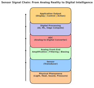
In today’s electronics ecosystem, conversations are dominated by artificial intelligence, edge computing, and ultra-fast wireless networks. Yet, behind every groundbreaking innovation, there lies a quieter but indispensable player i.e., analog electronics. While digital may dominate headlines, it is analog that ensures real-world phenomena which can be captured, conditioned, and processed.
As engineers often remind themselves, “Nature is analog. Everything else is an approximation.” No matter how sophisticated a digital system is, its accuracy and reliability hinge on the quality of the analog front-end. From radar in advanced driver-assistance systems (ADAS) to MEMS accelerometers in smartphones, and from biomedical wearables to industrial IoT nodes, analog electronics forms the first link in the sensor signal chain.
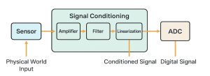
Why All Sensors Speak Analog First
Every physical phenomenon light intensity, sound waves, heat, vibration, or radio frequency (RF) radiation exists in analog form. Sensors are essentially transducers, converting these continuous signals into measurable electrical quantities. But before such data can be digitized and analyzed by processors or AI algorithms, it must pass through an analog front-end (AFE).
The AFE includes key blocks such as instrumentation amplifiers, filters, linearization circuits, and signal conditioning modules that prepare raw sensor outputs for analog-to-digital conversion (ADC). Without robust analog conditioning, even the most advanced digital processors would be “blind” to the real world.
As Walt Maclay, CEO of Voler Systems, puts it: “Digital processing is only as good as the analog electronics feeding it. Garbage in, garbage out applies more to sensors than anywhere else.”
Core Functions of Analog in Modern Sensors
- Signal Amplification
Many sensors output signals in the microvolt or millivolt range, easily drowned by noise. Instrumentation amplifiers and low-noise amplifiers (LNAs) boost these signals while preserving fidelity. For example, electrocardiogram (ECG) sensors require amplifiers with high common-mode rejection ratios (CMRR) to extract meaningful heart signals from noise-laden environments. - Filtering
Real-world signals are messy. Analog active and passive filters remove unwanted noise and interference before digitization. In radar systems, bandpass filters ensure only the target frequency range is processed, dramatically improving signal-to-noise ratio (SNR). - Linearization & Biasing
Many sensor outputs are nonlinear by nature. Analog circuits implement linearization techniques that correct these distortions, making sensor behavior predictable. Similarly, biasing ensures transducers operate in optimal ranges. For example, in thermistors, resistance-to-temperature curves must be linearized before meaningful temperature data is derived. - Conversion Readiness
Analog circuits prepare signals for ADC compatibility by ensuring proper voltage levels, impedance matching, and bandwidth. Without this step, digitization could lead to clipping, aliasing, or resolution loss.
Case Studies: Analog at Work in Emerging Applications
- Automotive ADAS
ADAS relies heavily on radar and LiDAR sensors, where real-time performance is non-negotiable. Analog front-ends amplify weak RF echoes, filter them for interference, and feed precise signals to high-speed ADCs. Even a microsecond delay can mean the difference between safe braking and a collision.
- Biomedical Devices
Wearable medical devices like glucose monitors and ECG patches demand ultra-low-power, high-precision analog circuits. Here, analog electronics extend battery life while ensuring clinical-grade accuracy. An error of even 1 mV in amplification could translate into misdiagnosis.
- Industrial IoT
Factories rely on thousands of sensors for vibration monitoring, predictive maintenance, and process automation. Analog circuits in these environments must withstand electrical noise, temperature fluctuations, and mechanical stress. Unlike fragile digital logic, robust analog designs ensure reliability under extreme industrial conditions.
- Environmental Monitoring
Long-term stability is critical in air-quality monitors, soil sensors, or weather stations. Analog circuits designed for low drift and high linearity guarantee consistent data for years without recalibration.
Analog’s Edge Over Digital in Certain Tasks
While digital processing offers flexibility, analog holds an edge in critical aspects:
- Zero Latency: Analog signals propagate at the speed of physics — no clock cycles required. For radar-based collision avoidance, this deterministic performance is irreplaceable.
- Power Efficiency: Analog front-ends consume far less power than equivalent digital circuits, making them essential in wearables and IoT nodes where every microamp counts.
- Reliability under Harsh Conditions: Analog circuits continue functioning in extreme environments — radiation, high temperatures, or electromagnetic interference — where digital logic often fails.
As Bob Dobkin, co-founder of Linear Technology, famously said: “Analog will never die, because the world is analog.”
Integration Trends: Analog in the Age of SoCs and SiPs
The industry is increasingly moving towards system-on-chips (SoCs) and system-in-packages (SiPs) that integrate both analog and digital functions. For instance, today’s MEMS inertial sensors often include on-chip AFEs, ADCs, and digital processors in a single package. This integration reduces footprint, improves signal integrity, and supports miniaturization for wearables, drones, and autonomous systems.
However, integration does not eliminate the need for analog expertise. Instead, it requires engineers to design mixed-signal systems where the interplay between analog and digital domains is carefully managed. Issues like thermal drift, bandwidth matching, and parasitic effects remain squarely in the analog domain.
Conclusion: Analog as the Permanent Foundation
In the race towards digital transformation, analog electronics is often overlooked. Yet, it is precisely analog that determines how effectively digital systems can sense and respond to the physical world. Whether in self-driving cars, medical diagnostics, or industrial automation, analog remains the timeless backbone of modern sensors.
For engineers, the message is clear: mastering analog design is not a relic skill, but a future-proof investment. The more complex and interconnected systems become, the more critical it is to ensure rock-solid analog foundations.
As the electronics pioneer Barrie Gilbert once noted: “You can digitize data, but you cannot digitize reality. Reality is, and will always be, analog.”
The post Analog Electronics: The Timeless Backbone of Modern Sensors appeared first on ELE Times.
A 6 mosfet module I made for breadboard use
 | I was playing with 12v LED cob panels and wanted to drive them from a esp32 on breadboard. So i made this, with 6 2N7000 mosfets and the associated resistors. I was quite pleased with my happy notion of alternating the orientation of the transitors alternately so the sources were all in a line, this also made the drains form neat pairs. which was nice. [link] [comments] |
Very simple TCI ignition system
 | Hello everyone, Chris here. I built a simple TCI ignition module, and it works— but I haven’t tested it yet on a motorcycle or anything else. My friend said he had done this before on a classic car and it worked. I’ve uploaded a full tutorial video with the circuit and parts on YouTube. You can check it out and let me know what you think— I’ll put the link in the comments. [link] [comments] |
Third party (non-AIB) Video card pcb with its chip removed
 Video card pcb with its chip removed") | submitted by /u/computune [link] [comments] |
Сторінки


![[link]](https://i.redd.it/2bfbx0zxcbpf1.jpeg)
![[link]](https://i.redd.it/i420ujjaw8pf1.jpeg)
![[link]](https://i.redd.it/8tdtdsobzyof1.png)