
Збирач потоків
Wise Integration launches first digital controller for GaN totem-pole PFC
КПІ ім. Ігоря Сікорського співпрацюватиме з N-iX

КПІ ім. Ігоря Сікорського співпрацюватиме з N-iX — глобальною компанією, що спеціалізується на розробці програмного забезпечення та IT-консалтингу, допомагаючи бізнесам з усього світу створювати успішні продукти.
Пріоритетні напрями співпраці:
Oscilloscope input coupling: Which input termination should be used?

Getting signals into an oscilloscope or digitizer without distorting them is a significant concern for instrument designers and users. The critical first point in an instrument is the input port. Oscilloscopes offer 50-Ω and 1-MΩ input terminations for both channels and trigger inputs. When should each be used?
A typical oscilloscope offers input ports terminated in either a 50-Ω, DC-coupled, or 1-MΩ AC- or DC-coupled, or ground (Figure 1).
 Figure 1 The input coupling choices for a typical oscilloscope include 50-Ω DC, 1-MΩ AC or DC, and ground. Source: Art Pini
The 50-Ω termination is intended for use with 50-Ω sources connected to the oscilloscope using a 50-Ω coaxial cable. The 50-Ω input properly terminates the coaxial cable, preventing reflections and associated signal losses.
The 50-Ω input termination is also used with certain probes. The simplest probe, based on a 50-Ω termination, is the transmission line or low-capacitance probe (Figure 2).

Figure 2 The low capacitance probe is intended to probe low impedance sources like transmission lines. A 10:1 attenuation is achieved by making RIN equal 450 Ω, which results in a 10:1 attenuation of the probed signal. Source: Art Pini
The transmission line probe has a relatively wide bandwidth, typically ranging from 5 GHz or more. Its input impedance is low, and in the case of a 10:1 probe, it is only about 500 Ω. Most other active high-bandwidth probes also utilize the 50-Ω oscilloscope input termination.
The 1-MΩ input termination is intended to connect to 10:1 high-impedance passive probes as shown in Figure 3.

Figure 3 A simplified schematic for a 10:1 high impedance passive probe connected to an oscilloscope’s 1 MΩ input. Source: Art Pini
The high-impedance probe places a 9-MΩ resistor in series with the oscilloscope’s 1-MΩ input termination, forming a 10:1 attenuator. This passive probe has a DC input resistance of 10 MΩ. The compensation capacitor (Ccomp) is adjusted so that the time constants Rin*Cin are the same as Ro*(Co+Ccomp), forming an all-pass filter offering a relatively square low-frequency pulse response. The 1-MΩ termination also serves as a high-impedance input for low-frequency measurements, where reflections are not an issue.
50-Ω vs 1-MΩ inputsThe two input terminations have significant differences. Consider the Teledyne LeCroy HDO 6104B, a 1 GHz mid-range oscilloscope, as an example (Table 1).
|
Input Termination |
Bandwidth |
Coupling |
Vertical Range (V/div) |
Offset Range |
Maximum Input |
|
50 Ω |
1 GHz |
DC, GND |
1 mV to 1 V |
± 1.6 V to ±10 V |
5 Vrms, ± 10 V p-p |
|
1 MΩ |
500 MHz |
AC, DC, GND |
1 m V to 10 V |
± 1.6 V to ± 400 V |
400 V(DC + Peak AC<10 kHz) |
Table 1 The characteristics of the input terminations are quite different. Source: Art Pini
The bandwidth of the 50-Ω termination is usually much greater than that of the 1-MΩ termination. In this example, it is 1 GHz. The oscilloscope’s bandwidth is generally specified for the 50-Ω termination. The 50-Ω input has a more limited input voltage range than the 1-MΩ input. The maximum voltage range of the 50-Ω termination is power-limited to 5 Vrms by the ½-watt rating of the input resistor. The 1-MΩ has a maximum voltage rating of 400 V (DC+AC peak <10 kHz). The 50-Ω input is only available in DC-coupled mode, whereas the 1-MΩ termination is available in both AC and DC-coupled modes. Finally, the offset range of the 1-MΩ input extends up to ±400 V while the 50-Ω offset range is ±10 V.
DC or AC input couplingDC coupling applies to the entire frequency spectrum of the signal’s frequency components from DC to the full rated bandwidth of the instrument’s specified input. AC coupling filters out the DC by placing a blocking capacitor in series with the oscilloscope input. The series capacitor acts like a high-pass filter.
In most oscilloscopes, the AC-coupled input has a lower cutoff frequency of about 10 Hz. AC-coupling the 50-Ω termination would require about 20,000 times larger capacitors to achieve the same 10-Hz lower cutoff frequency, so it is not done. This ability to separate a signal’s AC and DC components is utilized in applications such as measuring ripple voltage at the power supply’s output. The AC coupling blocks the power supply’s DC output while passing the ripple voltage. Figure 4 compares an AC- and a DC-coupled waveform with an offset voltage.

Figure 4 A 1 MHz, 381 mVpp, signal with a 100-mV DC offset is acquired using both DC (top trace) and AC (lower trace) coupling. Source: Art Pini
The upper trace shows the DC-coupled waveform. Note that the DC offset shifts the AC component of the input signal upward while the AC signal, shown in the lower trace, has a zero mean value. The AC coupling has removed the DC offset.
The peak-to-peak amplitude is measured using measurement parameter P1 as 381 mV. They are identical because the offset of the DC-coupled signal is canceled by the subtraction operation used in calculating the peak-to-peak value.
The DC-coupled signal has a DC offset of 100 mV, measured by the mean measurement parameters P2. The AC-coupled signal has the same peak-to-peak amplitude (P5) but a mean(P6) of near-zero V. The AC-coupled signal’s RMS amplitude (P3) reads 167.5 V because it includes the RMS value of the DC offset. The RMS value of the AC-coupled signal (P7) reads 134.4 mV because the mean value is zero. The DC-coupled signal’s standard deviation (sdev) (P4) is identical to the RMS values of the AC-coupled signal. Since the standard deviation calculation subtracts the mean value of the signal from the instantaneous value before computing RMS, the standard deviation is sometimes referred to as the AC RMS value.
Trigger input termination and couplingThe trigger input is another oscilloscope input that must be considered as it affects the instrument’s triggering. It is derived from one of the input channels, the external trigger input, or the power line. The trigger coupling for any of the inputs other than line is one of four possibilities: AC, DC, low-frequency reject (LF REJ), or high-frequency reject (HF REJ) (Figure 5).

Figure 5 The trigger input coupling selections include two bandwidth-limited modes (LF and HF REJ) and AC- and DC-coupling. Source: Art Pini
The AC and DC coupling perform as the AC and DC input coupling selections. LF REJ is an AC coupling mode with a high-pass filter in series with the trigger input. HF REJ is DC coupled with a low-pass filter in series with the trigger input. The cutoff frequencies of high-pass and low-pass filters are usually about 50 kHz. The LF and HF REJ coupling modes are usually used for noisy trigger signals, which might be encountered when testing switched-mode power supplies.
If the trigger input source is one of the input channels, then the trigger input inherits the termination impedance of the input channel. If the external trigger input is used, the input impedance can be selected (Figure 6).

Figure 6 The termination of the external trigger input includes both 50-Ω and 1-MΩ DC, along with a 1:1 and a 10:1 attenuator. Source: Art Pini
The termination is either 50 Ω or 1 MΩ. The external trigger is DC-coupled from the physical input to termination. The trigger coupling selection sets the coupling between the termination and the trigger.
Selecting input terminations when using a probeMost modern oscilloscopes have intelligent probe interfaces that sense the probe’s presence and read its characteristics. The instrument adjusts the input termination and attenuation to match the probe’s requirements. For classical passive probes, simpler probe interfaces sense the probe’s sense pin to detect its presence and attenuation and set the instrument coupling and attenuation to match the probe. If the passive probe lacks a sense pin or an intelligent interface, then the attenuation setting of the input channel must be done manually.
50-Ω termination workaroundsThe 50-Ω termination offers the highest bandwidth and is used with signal sources connected via 50-Ω coaxial cables or active probes that expect a 50-Ω termination. Serial in-line attenuations can be used to increase the voltage range of the 50-Ω input. AC coupling of the 50-Ω input can be accomplished using an external blocking capacitor. The lower frequency cutoff will be a function of the block’s capacitance.
Other traditional terminating impedances can be adapted to the 50-Ω termination by using an external in-line impedance pad. This is particularly common in applications such as video, where 75-Ω terminations are the standard. If an impedance pad is used, the pad’s attenuation has to be manually entered into the input channel setup.
1-MΩ termination workaroundsThe 1-MΩ termination provides a high input impedance, which reduces circuit loading. It offers the highest voltage and offset ranges, but its bandwidth is restricted to 500 MHz or less. Care should be exercised when using it to measure low-impedance sources with frequencies greater than 40 to 50 MHz to avoid reflections, which will manifest themselves as ringing (Figure 7).

Figure 7 Measuring a low-impedance source using a 1-MΩ input can result in reflections that look like ringing (upper trace). Using a 50-Ω termination (lower trace) does not show the problem. Source: Art Pini
If you must use a 1-MΩ input, reflections can be reduced by soldering a 50-Ω resistor to the low-impedance source and connecting the 1-MΩ input to the resistor. This will help reduce reflections from the high-impedance termination back to the source.
The rail probe is the best of all possible worldsGiven that a typical application of oscilloscopes is measuring power supply ripple, the DC-coupled input’s limited offset voltages and the AC-coupled inputs’ attenuation call for a unique solution. The rail probe is a solution to measuring ripple on power rails that offers a large built-in offset, low attenuation, and high DC input impedance. The rail probe’s built-in offset and low attenuation permit the rail voltage to be offset in the oscilloscope by its mean DC voltage with high oscilloscope vertical sensitivity, achieving a noise-free view of small signal variations. The high DC input impedance eliminates the loading of the DC rail.
The input termination and coupling are important when setting up a measurement. Keep in mind how they can affect the signal acquisition and subsequent analysis.
Arthur Pini is a technical support specialist and electrical engineer with over 50 years of experience in electronics test and measurement.
Related Content
- Terminating a differential-input signal
- It’s not just 50 Ω: Some termination tips for differential and single-ended amplifiers
- Getting EMC design right – First time, Part 4: Terminations & Parts placement
- Digitizer front ends need the right inputs
- Build your own oscilloscope probes for power measurements (part 1)
- Basic oscilloscope operation
- Measure small impedances with Rogowski current probes
The post Oscilloscope input coupling: Which input termination should be used? appeared first on EDN.
A nostalgic technology parade of classic amplifiers

There are numerous evergreen chips in the semiconductor industry, and this blog provides a sneak peek at some of these timeless technology marvels. Take µPC1237, for instance, NEC’s bipolar analog IC, which is still used in stereo audio power amplifiers and loudspeakers. Then, there is Toshiba’s fabled TA7317P, another classic IC used for power amplifier protection. The blog highlights the inner workings of these awesome chips and expands on why they are still in play.
Read the full blog on EDN’s sister publication, Planet Analog.
Related Content
- Audio amplifier selection in hearable designs
- Reference board exemplifies audio amplifier silicon
- Audio amplifier basics: Select the best topology for your design
- Audio amplifiers, class-T, class-W, class-I, class-TD and class-BS
- The NA1150 audio amplifier sets a new standard, driving speakers with PWM
The post A nostalgic technology parade of classic amplifiers appeared first on EDN.
KYOCERA AVX Releases Robust new Series of Vertical-Mating Battery Connectors
The new 9155-900 Series 2.5mm-pitch vertical-mate battery connectors provide engineers in the industrial, automotive, datacom, household appliance, and consumer electronics markets with robust, reliable, and user-friendly power connectivity solutions.
KYOCERA AVX, a leading global manufacturer of advanced electronic components engineered to accelerate technological innovation and build a better future, has further expanded its industry-leading selection of standard battery connectors with the introduction of the new 9155-900 Series 2.5mm-pitch vertical-mate battery connectors.
The new 9155-900 Series 2.5mm-pitch vertical-mate battery connectors feature a unique contact geometry that deflects cleanly when a module, battery pack, mating connector, or PCB is vertically pushed into position, enabling full vertical engagement without the risk of contact damage. Traditional right-angle battery connectors require users to engage the contacts by inserting the mating module or battery pack at an angle before rotating it into position to reliably prevent contact damage that could negatively impact connector performance and lifetime. The 9155-900 Series does not. Infact, users can mate these connectors from any angle without inadvertently damaging the contacts, ensuring high-integrity connections regardless of user experience or skill level.
The 9155-900 Series 2.5mm-pitch vertical-mate battery connectors feature an extremely forgiving sweeping beam contact design and an anti-snag feature that reliably protects the contacts from damage during deflection, as well as when static. The series also features ultra-robust and -reliable gold-plated beryllium copper (BeCu) contacts that deliver excellent electrical and mechanical performance for up to 5,000 mating cycles and optional plastic locating bosses and solder tabs that maximize the mechanical stability of the connector in high-shock and vibration environments, like automotive applications.
The series features flame-retardant (UL94 V-0) black, glass-filled Nylon 46 insulators, two to six BeCu contacts with either 0.4µm or 0.8µm of selective gold-over-nickel plating (the former of which is suitable for most commercial and industrial applications and the latter of which is suitable for harsh-environment applications), and pure tin tails. They are rated for 500VACRMS or the DC equivalent, up to 3A, and operating temperatures extending from -40°C to +125°C. They are also REACH and RoHS compliant and shipped in tape and reel packaging in quantities of 800 for automated pick and place assembly.
Ideal applications for the new 9155-900 Series 2.5mm-pitch vertical-mate battery connectors extend throughout the industrial, automotive, datacom, household appliance, and consumer electronics markets and include handheld and portable industrial and consumer electronics devices that require docking or cradling, such as charging stations, internet and home appliances that require battery backup, and automotive applications that require the easy installation and removal of modules or battery packs, ranging from headsets, gaming controllers, and walkie talkies to automotive cooling fans.
“Traditional right-angle battery connectors with exposed contacts require pluggable modules to be inserted at an angle and then gently rotated into position to prevent contact damage. And while that may seem insignificant, the extra step required to safely and successfully mate traditional battery connectors increases the potential for mismating by half,” said Perrin Hardee, Product Marketing Manager at KYOCERA AVX. “Our new 9155-900 Series 2.5mm-pitch vertical-mate battery connectors are engineered to ensure proper mating from any angle and eliminate the possibility of inadvertently damaging the contacts during the process—regardless of user experience or skill level. They’re also compact and robust enough to withstand automotive levels of shock and vibration.”
The post KYOCERA AVX Releases Robust new Series of Vertical-Mating Battery Connectors appeared first on ELE Times.
Vishay Intertechnology CHA Series of AEC-Q200 Qualified Thin Film Chip Resistors Now Available in 0402 Case Size
CHA0402 Microwave Resistors Deliver Stable High Frequency Performance Up to 50 GHz Under Harsh Environmental Conditions
Vishay Intertechnology, Inc. announced that it has expanded its CHA Series of AEC-Q200 qualified thin film chip resistors with new devices in the 0402case size. Available with a wide range of resistance values from 10 Ω to 500 Ω, CHA0402 resistors provide high frequency performance up to 50 GHz for automotive, telecom, medical, space, avionics, and military applications.
Now available in the 02016 and 0402 case sizes, CHA series devices offer very low internal reactance and exhibit behavior close to a pure resistor over their large frequency range, with a nearly flat Z/R curve to 70 GHz and 50 GHz, respectively. The microwave resistors maintain their high frequency stability even after the most stressful AEC-Q200 tests — validated by their ΔR and Z/R measurements — guaranteeing high performance under harsh environmental conditions.
The CHA series is ideal for automotive ADAS, LIDAR, connectivity, and 4D radar systems; LEO satellites and space communication systems; X-ray, MRI, and CAT scan machines; 5G / 6G telecommunications equipment, base stations, and repeaters; military guidance and telemetry systems; drones; and RF antennas. For these applications, the CHA0402 resistors provide limiting voltage of 37 V, rated power of 300 mW at +70 °C, and a temperature coefficient of ± 100 ppm/°C, with ± 50 ppm/°C available on request.
To reduce development time and costs, the devices’ S-parameter data is available for electronic simulation, in addition to 3D models for Ansys HFSS, Modelithics Microwave Global Models (PCB and pad-scalable), and design kits. RoHS-compliant, halogen-free, and Vishay Green, the resistors are offered in waffle pack and tape and reel packaging.
The post Vishay Intertechnology CHA Series of AEC-Q200 Qualified Thin Film Chip Resistors Now Available in 0402 Case Size appeared first on ELE Times.
EFFECT Photonics raises extra $24m in Series D funding round
Innoscience and Midea partner to accelerate GaN adoption in home appliance industry
BluGlass closes share purchase plan, raising a further $5.3m
A Record Year for the 75th Annual IEEE Electronic Components and Technology Conference (ECTC)
Among the Highlights were Special Sessions Detailing the Status and Future Directions of Technology in Key Areas
The 75th annual 2025 IEEE Electronic Components and Technology Conference (ECTC), held at the Gaylord Texan Resort & Convention Center here May 27-30, had record attendance, a record number of paper submissions/presentations, record international and student participation, and a record number of exhibitors in a sold-out exhibition hall:
- 2,518 attendees, the highest in the conference’s 75-year history and a significant increase over the 2,008 who attended last year, which itself was a record.
- The number of abstracts submitted was the highest ever (775), as were the 390 technical papers presented in 36 oral and 5 interactive presentation sessions, including one dedicated to students.
- Several paper presentations attracted more than 600 attendees, as sessions on topics of intense industry interest – such as hybrid bonding– were standing-room only.
- 16 professional development courses were attended by 596 participants.
- There were speakers from more than 20 countries globally.
- There was a record level of industry support, with 51 corporate sponsors and 138 booths in the exhibit hall.
Among the highlights were 11 Special Sessions. In these, panels of industry experts discussed the present status and future roadmaps of technologies essential for artificial intelligence (AI), high-performance computing (HPC) and other fast-growing, evolving applications.
“Advanced chip packaging technologies are essential for the development of the electronics industry, and the ECTC conference has long been the world’s leading forum for advancements in microelectronics packaging and component science and technology,” said Przemyslaw Gromala, ECTC 2025 Program Chair and Chief Expert/R&D Project Leader at Robert Bosch GmbH. “ECTC serves as a collaborative global platform for exploring cutting-edge advancements in microelectronic packaging, fostering innovation and addressing key industry challenges. This year’s Special Sessions offered a rich selection of compelling topics and expert panelists.”
Here are highlights from three of the ECTC 2025 Special Sessions:
Advanced Materials for Enabling Co-Packaged Optics Integration – This Special Session was co-Chaired by Karan Bhangaonkar (Google) and Vidya Jayaram (Chipletz). Panelists were Mark Gerber (ASE), Z. Rena Huang (Rennselaer Polytechnic Inst.); Padraic Morrissey (Tyndall National Inst.), Kumar Abhishek Singh (Intel) and Christopher Striemer (AIM Photonics).
As modern computing strives for higher performance, co-packaged optics or CPO (i.e., the integration of optics and electronics on a substrate) is emerging as a solution to meet computing/communication demands for high bandwidth at low power. The innovations, challenges and future needs to realize CPO technology were discussed in this Special Session.
Gerber from ASE gave an overview of the system requirements that are driving CPO material considerations, noting that heat can have significant effects on photonic integrated circuits. He also identified other issues that increase thermal sensitivities in CPO architectures, such as flux outgassing, and described why the order in which assembly steps occur also has an impact.
Huang from RPI said that while much work is taking place to understand and address CPO packaging considerations, much more progress is needed, especially for AI chiplets for large-language models (LLMs), where the key concerns are speed, power and efficiency. She discussed the possibility to build optical networks on optical interposers/wafers/panels, noting that large chiplets could be optically connected with optical interposers, using optical waveguides to reduce loss.
Morrissey from Tyndall said that for optimum CPO performance, the optics must be moved closer to the edge of compute, and glass has great potential for use as a substrate because it’s optically transparent, has good RF behavior, and lends itself to fabricating high-quality vias. Glass also can work beyond wafers and with really large panels, he said, and can lead to pluggable connectivity. However, he noted that heat is an issue with glass.
Singh from Intel said CPO isn’t just desirable, it’s absolutely necessary to scale-up advanced packaging. He noted that CPO allows both edge and vertical interconnects, meaning there are many areas where materials come into play. He said that while CPO architectures face unique challenges – such as foreign particles blocking the light path – they also face many of the same issues as non-CPO architectures, such as misalignment and cracks. But these challenges bring opportunities to advance the state-of-the-art.
Striemer from Aim Photonics described why optically active materials will drive CPO, and also outlined the need for passive material innovations such as 3D printing and novel designs like suspended structures, although right now it’s unclear which ones will offer the most benefit.
Hybrid Bonding (HB): to B, or not to B? Needs and challenges for the next decade – This Special Session was co-Chaired by Benson Chan (Binghamton Univ.), Masha Gorchichko (Applied Materials) and Dishit Parekh (AMD). The panelists were Su Jin Ahn (Samsung), Anne Jourdain (imec), Chet Lenox (KLA), Laura Mirkarimi (Adeia), Masao Tomikawa (Toray Ind.) and Brett Wilkerson (AMD).
Hybrid bonding is the key technology for high-density 3D integration and advanced packaging, and in recent years, significant advancements were made in pitch scaling, die-to-die bonding, alternative materials, and low-temperature processes. But many engineering and technological challenges remain, such as defectivity, metrology, design challenges, and cost. This panel summarized recent advancements in HB, identified the most pressing issues limiting its adoption for mainstream electronics, and outlined its likely development over the next decade.
Gorchichko from Applied noted the different types of HB (wafer-wafer, die-wafer, die-die) and said that while HB debuted about 10 years ago in an image sensor from Sony, today the focus is on integrating DRAM memory. She said that advanced metrology is key, because we are now talking about molecular bonds, and therefore an understanding of all the relevant chemical and mechanical requirements is needed. Moreover, to get higher yields and more throughput, not just better but also faster metrology is needed. She noted that thermal concerns are an issue with increasing power density.
Su Jin Ahn from Samsung outlined major HB technology issues and challenges. One is that the many process steps required leave particles on the bonding surface, leading to potential failure. Another is that for AI, the wider, thinner dies used degrade bonding and lead to quality issues. She said what’s needed are advanced metrology/inspection tools and methods, along with design/process co-optimization for bonding. She said the main driver going forward is the need to combine chip and packaging technologies.
Jourdain from imec emphasized the need for fast, reliable metrology solutions, and discussed the pros and cons of copper interconnect and barrier metals.
Lenox from KLA noted the many needs and challenges that come with HB – interposers, warpage control, dielectric interface profiles, clean singulation, bonding alignment – and said that while HB is important, there are other less complex and costly technologies that might preclude the need for HB, such as bridges. He also said that HB creates a need for advanced metrology and inspection capabilities all the way from the front end to packaging.
Mirkarimi from Adeia focused on three areas: metrology improvements for improved throughput and yield; the evolution of 2.5D/3.5D HB packaging technology; and thermal solutions for high power-density chipsets. With regard to metrology, she noted that HB architectural complexity demands a reliable “health of the line” metrology protocol for all process steps. Also, better ways to understand nanoscale topography and to detect surface defects are needed, as are ways to rework HB to reduce costs, such as bond energy engineering. Regarding HB packaging trends and challenges, she said that ultra-high bandwidth, inter-die communication at a 1µm die-to-wafer pitch will require system simplification, such as bonding dies directly to the substrate or using bridge dies to replace an interposer. For thermal management, she described a potential cooling solution that makes use of an integrated manifold and a cold plate bonded to an IC, among other features, and which can be custom-designed to manage specific heat maps.
Tomikawa from Toray said that as the need to bond chips to interposers increases, the need for HB processes that make use of polyimide (PI) resin will become more apparent. That’s because PI enables low-temperature, low-pressure HB processes which minimize warpage and device damage. Many challenges remain, though – precise copper protrusion control and low-temperature copper diffusion bonding are key factors for success.
Wilkerson from AMD spoke from a product perspective. He pointed out that HB requires complex processing. much time and many expensive fab processes, and that it can take several weeks to accomplish, which impacts a company’s time-to-market capabilities. He said thermal resistance is a critical issue, and that there’s a need for standards for the use of HB for memory integration with silicon.
Thermal Management Solutions for Next-Generation Backside Power Delivery – This Special Session was co-Chaired by Dwayne R. Shirley (Marvell) and Tiwei Wei (Purdue University/UCLA). The panelists were Muhannad Bakir (Georgia Tech), Dureseti Chidambarrao (IBM) and Herman Oprins (imec).
The increasing power density and thermal challenges in advanced semiconductor packaging have led to the development of backside power delivery (BPD) technology, where the power delivery network is relocated from the frontside to the backside of a silicon wafer. While it enhances power efficiency, performance, and design flexibility, BPD also introduces thermal management challenges and the need for innovative cooling solutions. Participants in this Special Session discussed the latest advancements and challenges in thermal management for next-generation BPD.
Bakir from Georgia Tech said that for 3D architectures, interlayer cooling is needed, but asked, how do we enable high-density interconnect within such a structure? He said the solution is to fabricate through-silicon via (TSV) structures with integrated cooling, electrical conductivity, and power, using vertical vias. He addressed the many issues that such a design brings – aspect ratios, TSV heights, etc.
Chidambarrao from IBM said that because there are lots of subtleties with BPD architectures, reducing the problem to important basics and solving it with enough accuracy is key. He noted that chip complexity significantly impacts thermal conductivity, and that level-to-level differences can be quite large. He said that an understanding of the entire chip overlay is needed, because there are tricky hot spots, and he described IBM’s strategy, which is to use machine learning plus FEA modeling to calculate the average properties of multiple levels together. He noted that BPD issues only become worse with 3D architectures.
Oprins from imec said it is absolutely critical to identify the basic problems with each particular BPD architecture, because there are so many different flavors of BPD.
Wei from Purdue/UCLA said that bond interfaces drive thermal impacts, and she gave an overview of research into different ways to deal with this issue, encompassing factors such as die thickness, CMOS-compatible structures like air gaps or glass bridges, trenches, copper/diamond microbump bonding, two-layer microchannel structures (i.e. manifolds), and others.
The post A Record Year for the 75th Annual IEEE Electronic Components and Technology Conference (ECTC) appeared first on ELE Times.
Validating the O-RAN Radio: From Silicon to Smart Networks
Author: Ajay Kumar, R&D Principal FPGA Engineer, Keysight Technologies
The Open Radio Access Network (O-RAN) Alliance led by a group of mobile network operators (MNOs), has been the driving force for the evolution of 5G Radio Access Network (RAN). The aim is to steer the industry towards more open, interoperable, virtualized, and intelligent architecture. This article outlines the crucial validation steps needed to bring O-RAN radio from silicon to deployment-ready, secure and intelligent. It highlights the needs and challenges in pre- and post-silicon validation, multiple-input multiple-output (MIMO)/massive MIMO (mMIMO) performance verification, energy efficiency measurements, security testing, and radio management. To begin, let us explore the brief history, evolution, and architecture of the RAN.
Historically, RAN deployments have been dominated by proprietary hardware from a small group of vendors, leading to high cost and limited flexibility. O-RAN addresses these challenges by disaggregating the RAN architecture and introducing standardized interfaces for interoperability and virtualization. This open approach fosters flexibility enabling organizations to mix and match solutions from different vendors bringing down costs and promoting innovation.
In addition, recent advancements in artificial intelligence (AI) and machine learning (ML) are further enhancing O-RAN by making it more intelligent. This move will enable even more innovation when it comes to energy efficiency, enhancing security, network optimization, and maintenance of the network.
Key Components of O-RAN architecture
Figure 1 below breaks down the key components of O-RAN architecture which includes:
- O-RAN radio unit (O-RU): Performs analog/RF transmitter and receiver functions along with processing the lower part of the physical layer such as Fast Fourier Transform (FFT)/inverse FFT (IFFT), beamforming, precoding, cyclic prefix insertion/removal, and compression/decompression.
- O-RAN distributed unit (O-DU): Handles baseband processing, scheduling, radio link control, medium access control, and the upper part of the physical layer.
- O-RAN central unit (O-CU): A centralized and virtualized unit that is responsible for the packet data convergence protocol layer.
- O-RAN intelligent controller (O-RIC): Handles near real-time and non-real-time service to gather information from the network and uses artificial intelligence and machine learning to perform the necessary optimization tasks.
- Service Management and Orchestration (SMO): Manages and orchestrates the RAN centrally including both RICs.

Figure 1: O-RAN architecture with user equipment and core network.
The Radio Unit (RU) is a critical fronthaul component, providing wireless connectivity to user equipment. It communicates with the rest of the O-RAN components to transfer information to and from the core network. O-RAN alliance 7.2x split option redistributes physical layer functions between O-RU and O-DU to strike a balance between fronthaul bandwidth requirement, latencies and the complexity of the components. This influences the overall O-RU architecture of radio unit by adding signal processing functions to the digital part of the radio.
During the product development cycle, design teams validate functionality through block-level simulations. However, at the system level, simulation complexity and runtime increase dramatically. This makes it vital to initiate pre-silicon validation at the right stage and well before tape-out.
Pre-Silicon Validation to Build Confidence Before Tape-Out
Pre-silicon validation involves emulating the design before fabricating the chip to provide a more accurate representation of the design in real-world conditions. This step helps to achieve testing goals in a reasonable time span by identifying design flaws early on. However, to determine the required test cases for specific functions, a thorough understanding of the test specifications is required. These test specifications cover a wide variety of tests for control, user, synchronization and management (CUSM) plane protocols.
Creating test vectors that conform to 5G standards is a complex task, given the vast number of parameters involved. Adding to the challenge, these test stimuli need to be sent in a synchronous manner from both Ethernet interface on DU and either through the non-standardized time-domain IQ interface or the RF interface side for complete radio.
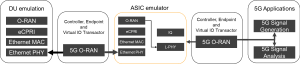
Figure 2: O-RU ASIC test protocol stack
To achieve the pre-silicon testing goals, it is important to have pre-verified test suites to avoid spending time debugging the test cases itself. Test setup observability is also of utmost importance in order to identify and resolve any issued early, and to prevent potential flaws from being carried over into the final taped out design. Figure 2 shows O-RU test protocol stack and controller test setup for ASIC emulation.
Post-Silicon Validation to Bridge Gap for Production
While the interoperability testing methodology, which involved testing the components together as a gNB, has remained largely consistent, conformance testing has evolved. Conformance testing ensures that each component adheres to specifications defined by the O-RAN Alliance.
To maintain momentum in the fast-paced design cycle, a smooth transition is required from pre-silicon to post-silicon validation. Hence, the same workflow and tools for signal generation and analysis are required to reuse the same test suite.

Figure 3: O-RU testing and validation test setup diagram and flow
In the post-silicon phase, testing access is primarily limited to the O-RAN and RF ports of the O-RU. To test O-RU, as illustrated in Figure 3, an O-DU emulator is required to send and receive CUSM-plane messages on O-RAN port, a vector signal analyzer to receive downlink RF signal sent by O-RU and a signal generator to send uplink signal to O-RU. Additional equipment may be required for non-conducted tests. All these test setup components are required to synchronize to common clock and work with-in tight fronthaul timing requirements.
MIMO and Massive MIMO to Achieve Desired Performance
MIMO and mMIMO technologies use multiple antennas – typically 16 or more for mMIMO systems, to serve multiple users simultaneously on the same frequency band. This increases spectral efficiency and throughput. With massive MIMO, advanced beamforming techniques need to be applied to steer radio signals precisely towards users to improve signal quality and reduce interference. However, as system complexity grows, performance validation can be highly complex, time-consuming and expensive.
To test massive MIMO radio unit, an O-DU emulator is required with tools to construct, play, capture and measure O-RAN traffic over ethernet interface; and multi-RF transceiver to generate the beams with noise and interference in different directions and receive at the same time. Test setups not only need to measure all beams and signals in uplink and downlink directions but also have the ability to pinpoint beamforming issues. Figure 4 shows an example of downlink beamforming with magnitude and phase weightings and corresponding beam patterns and EVM figures.
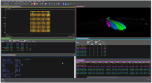
Figure 4: Downlink beamforming with magnitude and phase weightings and corresponding beam patterns, EVM figures
Energy Efficiency for Sustainability
With the exponential growth in wireless connectivity, energy efficiency has become a top priority for operators in order to reduce operational costs, achieve sustainability goals and reduce environmental impact. As many studies have shown that majority of energy is consumed by RAN, the O-RAN community is working on standardizing energy saving modes, with the goal to reduce power consumption without degrading the quality of service.
O-RU is the most power-hungry component in the access network. However, energy saving can be accomplished by numerous means such as variable clocking, dynamic power amplifier biasing, cell & carrier shutdown, RF channel reconfiguration, sleep modes, discontinuous transmission & reception. With the disaggregation of RAN, there is need to characterize each component to completely understand the trade-offs at system and network level. Figure 5 shows O-RU site power dissipation over a 24-hour period with and without microsleep enabled and potential savings.
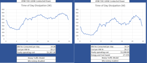
Figure 5: O-RU site power dissipation over a 24-hour period
Security Testing for Uninterrupted Radio Access
In a disaggregated, multivendor O-RAN environment, there are increased security risks for individual components, interfaces, network functions, and data. The O-RAN threat modeling and risk assessment specification includes over 160 distinct threats to these elements including O-RU.
Each element, protocol, and interface need to be scanned for vulnerabilities, stressed under real-world threat scenarios and checked for performance under simulated attacks. It is also important to ensure effective risk mitigation strategies are in place. With this in mind, automated security testing is critical, not only for compliance with security standards but to ensure guaranteed radio access, and alignment with O-RAN zero trust principles.
Radio Management with RIC for Operational Efficiencies
While the Service Management and Orchestration (SMO) layer handles the coordination of network resources, the RIC plays a key role in optimizing radio access network performance. The non-real-time RIC uses rApps to apply AI/ML-driven long-term optimization for less time sensitive operations. Whereas, the near-real-time RIC deploys xApps to make real-time network adjustments that are between ten milliseconds to one second.
Together, these controllers enhance network utilization and operational efficiency through advanced functions such as beam management and radio resource management. To ensure reliable performance, both open-loop and closed-loop strategies must be implemented and rigorously tested for continuous optimization.
Conclusion
The journey of O-RAN radio unit from silicon validation to smart networks is highly complex but essential to realize the full potential of open and intelligent networks. To keep up with accelerated design cycles and ensuring compliance with O-RAN fronthaul standards, it is essential to have well-planned test setups, robust tools, pre-verified test cases, and automated test suites to transition smoothly through different phases.
The post Validating the O-RAN Radio: From Silicon to Smart Networks appeared first on ELE Times.
Wise Integration Launches First Digital Controller, WiseWare 1.1, for GaN Totem Pole PFC with High Switching Frequency Up to 2 MHz
With WiseWare 1.1, GaN-Based Designs Achieve Compact Size and Peak Efficiency
Wise Integration, a pioneer in digital control for gallium nitride (GaN) and GaN IC-based power supplies, announced the release to production of its first fully digital controller, WiseWare 1.1 (WIW1101) based on the MCU 32 bits. This milestone innovation enables high-frequency operation up to 2 MHz, unlocking new levels of power density, efficiency, and form factor in compact AC-DC power converters. The product is now ready for volume production in customer-validated designs.
“This release marks a strategic milestone for Wise Integration’s roadmap,” said Thierry Bouchet, CEO of Wise Integration. “WiseWare 1.1 represents more than a product—it’s a key pillar in our vision to redefine power electronics through digital control. It strengthens our value proposition in high-density power conversion and reinforces our leadership as GaN technology scales to mass adoption.”
Digitally Driven, GaN Optimized
Unlike legacy analog solutions, WiseWare 1.1 leverages the speed and switching capabilities of GaN (gallium nitride) through a proprietary digital control algorithm in a MCU 32 bits, that enables zero voltage switching (ZVS) across all power transistors. Designed specifically for totem pole power-factor correction (PFC) architectures in critical-construction mode (CrCM), this controller allows engineers to dramatically reduce the size, weight, and thickness of magnetic components while maintaining >98 percent efficiency.
Customer-Proven Performance and Global Momentum
WiseWare 1.1 supports a broad power range from 100 W to 1.5 kW, making it suitable for a wide array of modern applications requiring both compactness and high energy efficiency.
Designed with flexibility in mind, WiseWare 1.1 works seamlessly with standard GaN across the full RDS(on) spectrum (drain-source on-resistance), giving power designers the freedom to choose the optimal transistor for each application—without compromising performance.
Typical applications include:
- High-efficiency AC-DC power converters,
- High-power density designs,
- Power supplies for servers,
- USB power delivery adapters for laptops and notebooks, and
- Switch-mode power supplies for monitors and displays.
The WiseWare 1.1 platform has already demonstrated robust market validation, with multiple customer design-ins and live demos at PCIM Europe, one of the industry’s most prominent power- electronics exhibitions. These demonstrations showcased 300W totem pole PFC converter boards using WiseWare 1.1 and WiseGan WI71060A transistors (RDS(on)=60mohms), operating from 90–264 VAC input to a 400 VDC output. At the same time, technical collaborations are progressing in Asia, reinforcing the company’s global reach.
Technical Highlights of WiseWare 1.1 (WIW1101)
- Switching frequency: up to 2 MHz
- Control mode: CrCM ensuring full ZVS
- Integrated protections: OCP, OVP, OTP, OPP
- Inrush management: no need for relay or thermistor
- Standby power: as low as 18 mW
- EMC-compliant demoboard with >98 percent efficiency
The post Wise Integration Launches First Digital Controller, WiseWare 1.1, for GaN Totem Pole PFC with High Switching Frequency Up to 2 MHz appeared first on ELE Times.
High-voltage bus converter power modules for electric vehicle 48V power delivery networks
Author: Maury Wood, VP Strategic Marketing
The economic and quality-of-life benefits of electrification is driving the adoption of HV to 48V DC-DC conversion across many markets. Integrated high-voltage to 48V power modules are becoming more common in EVs and other applications as battery voltages increase. Learn how bidirectional fixed-ratio bus converter modules are optimizing power delivery in these systems.
Bidirectional, power-dense DC–DC converters are the ideal solution for the new and challenging use cases presented by machine electrification across numerous industries. This paper demonstrates how high-efficiency, fixed-ratio DC–DC converter modules are capable of supporting transient regenerative loads without the cost and complexity of liquid cooling.
Electrification, the societal movement away from fossil fuel powered machines, is sweeping across all industrial, vehicle and aerospace/defense equipment categories. The economic and cultural forces driving this movement are well known and generally undisputed. Electrification has both environmental benefits (lower associated carbon emissions, for example) and key performance benefits such as high-torque motors enabling high levels of acceleration in electric vehicles.
High DC voltages ranging from 270V up to 1,000V are commonly used in electric equipment and vehicles as a means to reduce power losses in the bussing or cabling between the power source and the power load (linear and rotational motors, actuators, sensors, processors, point-of-load low voltage regulators, etc.). High voltages also enable the delivery of high levels of transduced mechanical force, both linear displacement and rotational displacement.
DC–DC converters play a vital role in transforming high voltages to lower voltages, with or without isolation, regulation and reverse operation, in electric vehicles, data centers, communications systems and industrial equipment of all types. These power converters can be implemented using discrete components or in modular package form. DC–DC converters power modules are the focus of this article.
Over the past 10 years or so, the dominant DC subsystem power delivery network (PDN) voltage of 12V has begun to transition to 48V (54V in data centers), driven by the significant increase in load power requirements, and the need to maintain safety extra-low voltage (SELV) levels, heralding the emergence of HV-to-48VDC converters. Coincident with this evolutionary change of subsystem PDN voltage has been the adoption of 48V-centric dc–dc converter power modules, which have numerous ease-of-use, power density, power scaling and weight benefits, and which support regeneration (the return of energy to the primary power source).
The use of high DC voltage is ramping in equipment, vehicles and infrastructure
Electrolytic batteries, using a fast-evolving variety of chemistries, are often used as both high-voltage and low-voltage dc power sources and are obviously ideal for mobile (non-tethered) and handheld applications. The rechargeable nature of many battery types, from lead acid cells to the latest sodium-ion and graphene types, as well as modern supercapacitors, support regenerative energy use cases that in aggregate are destined to save enormous amounts of energy globally.
In electric vehicles, it is common to see nominal battery pack voltages of 400VDC and 800VDC. In the future, 800V battery packs are likely to dominate, due to escalating energy density trends. Mild hybrid vehicles generally use 48VDC batteries, with some manufacturers electing to use 12VDC multi-cell packs. Electric vehicles include not only automobiles but also industrial and agricultural vehicles (including construction vehicles such as excavators and tractors) as well as all types of recreational vehicle platforms (personal watercraft, 4×4 off-road vehicles, snow machines, motorcycles, etc.). With few exceptions, notably driving range and the time required to refuel or recharge the vehicle, the electric versions of these vehicle types tend to have superior end-user performance (such as acceleration, torque and ride quality) than their internal combustion engine counterparts.
Why is 48VDC power distribution replacing 12VDC power distribution?
Higher distribution voltage delivers the same power with lower current. Because distribution power losses (typically using copper or aluminum busbars or cables) are a function of the square of the current (P = I2R), in high power applications these substantial conduction losses due to busbar and cable resistance can be reduced by using higher distribution voltages. Busbars and cables are sized according to current carrying capacity (referred to as ampacity), and a 4x increase in voltage and a 4x decrease in current has a substantial impact on sizing, weight and cost. For example, to conduct 200A, a copper busbar needs a cross-sectional area of about 0.0625 square inches, whereas to conduct 800A, a copper busbar needs a cross-sectional square of about 0.3125 square inches, a difference of a factor of five [3]. The size and weight of busbars and cabling associated with 48VDC are thinner, lighter and thus cheaper than those associated with 12VDC power delivery networks.
Exploring the capabilities of high voltage to 48V conversion with a fixed-ratio converter module
The technical capabilities of advanced 48V power modules unlock new levels of efficiency and performance. For example, the Vicor BCM6135 series is a family of fixed-ratio, isolated (4242V), bus converter power modules with integrated magnetics and by design are inherently bidirectional, supporting regenerative battery applications.
One member of this family, a 2.5kW steady-state-rated module, has a ratiometric conversion “K factor” (the equivalent of transformer turns ratio) of 1/16 and is rated to convert nominal 800V to nominal 50V.
Due to its circuit topology and zero-voltage and zero-current switching, its peak efficiency is 97.3%, resulting in 67.5W of power loss as heat (2.7% x 2.5kW) to thermally manage at peak power delivery (3.1kW) for a given case temperature of TCASE of 70°C. The volumetric power density is high at 159kW/L (module dimensions are 61.3mm by 35.4mm by 7.3mm); module weight is 58g, yielding a continuous massimetric power density of 43.1W/g.

Figure 1: BCM6135 Bus Converter Module.
The BCM6135 (see Figure 1) supports instantaneous bidirectional start-up and steady-state operation. Furthermore, the BCM6135 acts as a capacitance multiplier, scaling the bulk capacitance across the high-voltage (HI) bus to the low-voltage (LO) bus by the square of the K factor (162 = 256). This attribute saves the cost, weight and space of the bypass or bulk capacitors that otherwise would be required on the low-voltage bus.
Additionally, the high switching frequency of the BCM enables extremely fast load step transient (di/dt) performance of 8 MA/s, allowing the module to replace auxiliary batteries and supercapacitors otherwise needed to support the transient load steps in demanding applications, including those in high-performance computing and electric vehicles.
The BCM’s wide input voltage range (from 520V to 920V) supports a wide variety of DC voltage distribution standards. Wide input voltage range is one of the attributes of the proprietary Sine Amplitude Converter (SAC) topology used in the BCM. The importance of wide input voltage range is well illustrated by the recommendation of the German Association of the Automotive Industry, or VDA, VDA 320: Electric and Electronic Components in Motor Vehicles – 48V On-Board Power Supply–Requirements and Tests (version 01/20/2025), also known as LV 148, developed by the automotive OEMs Audi, BMW, Daimler, Porsche and Volkswagen as a common OEM standard for 48VDC voltage range components. This guidance recommends that the battery possess an unlimited voltage operating range between 36V and 52V, limited operating modes between 24V and 54V (see Figure 2).
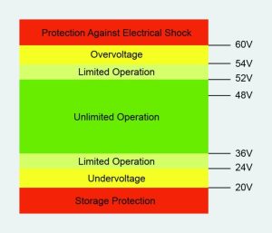
Figure 2: VDA 320 48VDC voltage range recommendation.
The thin (7.3mm) BCM6135 module family is overmolded and electroplated for thermal agility, shielded and interconnected through surface mount terminals or through-hole pins, and the three-dimensionally interconnected ChiP package offers low thermal impedance and high thermal adeptness, including a coplanar thermal interface to heat sinks and cold plates.
Regenerative active suspension without active cooling
The BCM6135 conversion efficiency at high ambient temperature (70°C) and sourcing 50A output current at 48V is typically 97.3%. This high-voltage to 48V power module is often used in continuous load applications, but it is also well suited to transient pulse load applications and depending on the pulse duty cycle of the load, potentially can be used with passive cooling (no forced air or liquid cooling). Regenerative electric vehicle active suspension (which can be combined with active anti-roll control) is an excellent example of a bidirectional use case that is characteristically transient. The linear motors that actuate the active suspension are activated only when bumps and potholes are encountered. This type of system application is best modeled and described using peak power conversion metrics.
In years past, 12VDC has been shown to be inadequate (within reasonable size, weight and cost constraints) to power active suspension motors. Note that an electric vehicle’s 800VDC main battery could be used to power an active suspension subsystem, but running 800VDC to the vehicle’s periphery reduces safety, particularly to first responders to crash accidents.
The guaranteed peak power rating of this BCM6135 model is 3.1kW for 20ms, with 25% duty cycle, at the low end of its operating voltage range (i.e., low line operation; the full continuous operating range is 17V to 57.5V). As can be expected, the peak power output derates for longer durations of the transient demand. Developing an application- level peak power specification for an active suspension is complex, as worst-case road surface profile, cooling method, size, weight and cost constraint goals can vary enormously. However, to minimize size, weight and cost, it is typically strongly preferred to use passive thermal management for the active suspension DC-DC converter subsystem (i.e., conductive/convective heatsinks but no fan forced air or circulating liquid cold-plates).
The design challenge to meet these constraints amounts to validating that the power converter module can meet the peak transient load demands without incurring thermally activated module shut down. The BCM6135 is electroplated on both sides, and the heat sink(s) should ideally contact both sides of the package. The module, which has a package thermal capacitance of 44.5 J/K, includes an internal temperature sensor, which in combination with the two sided thermal model, enables estimation of the maximum internal MOSFET “junction” temperature as shown in Figures 3 and 4.
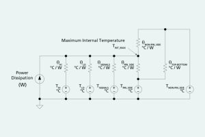
Figure 3: BCM6135 two-sided cooling thermal resistance model using electrical element
equivalence.

Figure 4: BCM6135 two-sided annotated thermal resistance model with element value annotation.
Estimation of internal module temperature profile
The thermal capacitance is used to calculate the thermal time constant of the module during a transient thermal event. This time constant is the product of thermal capacitance and thermal resistance. The value given for thermal capacitance in product datasheets is a calculated value that assumes the product is at a uniform temperature internally (throughout the module) at all times during the transient thermal event. This is a linearized simplification, but it allows the product designer a method to quickly estimate the temperature-versus-time behavior of the product early in the product design cycle. The simplification of uniform internal temperature also implies that the thermal time constant better reflects actual product performance when utilized for double-sided cooling of the 48V power module using heat sinks.
For example, an equivalent circuit to model the thermal resistance of the BCM6135 is shown in Figure 5. Electrical resistors are analogous to thermal resistances in units of degrees Celsius per watt [°C/W]. A current source is analogous to a heat source in units of watt [W]. A voltage source is analogous to a temperature source in this circuit model with units of degrees Celsius [°C].
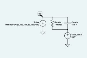
Figure 5: BCM6135 thermal model equivalent electrical circuit assumes package top and bottom cooling with an equivalent thermal resistance of 0.7°C/W and case temperature of 35°C.
The equivalent circuit assumes package top and bottom cooling with an equivalent thermal resistance of 0.7°C/W and case temperature of 35°C, thermal capacitance of the module of 44.5J/K, and that the module dissipates 130W during 30 seconds-on, 30 seconds-off continuously repeated pulses.
Simulation results for this circuit are shown in Figure 6; the operating conditions are 520 VHI, 32.5 VLO, 80A low-side peak output current (2.6kW peak output power). During the first power pulse, the maximum internal temperature increases to about 90°C. The next pulse shows an increase in maximum internal temperature to about 115°C. Repeated pulses would show maximum internal temperature remains around 115°C.
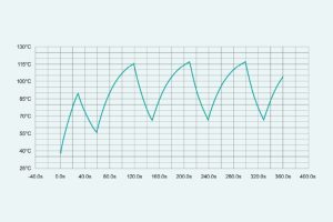
Figure 6: Simulated BCM pulsed power thermodynamics under the operating conditions 520 VHI, 32.5 VLO, 80A low-side peak output current. First power pulse shows the maximum internal temperature increases to about 90°C, followed by an increase to about 115°C. Repeated pulses would show maximum internal temperature limits to about 115°C.
Application testing of the module should always be conducted to validate initial modeled estimates of transient performance and to properly design a passive convective heatsink.
Lab test results
The BCM6135 is inherently bidirectional with instantaneous switching of the directional mode of operation. The conversion efficiency of the module is the same regardless of the direction of current flow.
In the regenerative active suspension application, the 800V battery is sourcing current when the vehicle is traveling over smooth road surfaces and the suspension actuation motor is the 48V load. When a pothole is encountered by the vehicle, the motors in the suspension momentarily become generators (compression), and the voltage on the low side of the BCM increases above the voltage of the 800V battery divided by the conversion K factor (K = 1/16 in this application). This difference in potential causes the bus converter to swap the direction of current flow, without internal loop controller intervention. The 800V battery then momentarily becomes the load (rebound) and recovers energy by charging through its battery management system circuit.
Once the displacement from the pothole has subsided, the bus converter will once again step down the 800V battery and supply current to the suspension linear motors. All of this occurs without intervention by the vehicle’s on-board processors. The frequency of these suspension actuations ranges from about 1Hz to 10Hz. Interestingly, the road surface profile is essentially an analog of the bus converter load step dynamics.
It is the potential difference between the bus converter high and low sides that defines the current amplitude and direction.
Imagine that the load on the low side is a passive load (such as a resistor) and on the high side there is a battery with a potential of 800V. The BCM will act as a K = 1/16 voltage transformer and create a potential on the low side equal to 50V. Current will flow through that resistor and is determined by voltage applied across the resistor.
If an energy source is added to the low side with potential of 51V and replaces the resistor, the potential difference between the output of BCM (50V) and that energy source (51V) will be negative (–1V), and the current will start flowing in the opposite direction. The level of this current will be defined by the total path resistance inside the BCM and the battery.
This can be visualized with the BCM connected to 800V source on the high side and a bidirectional power supply on the low side. By varying the voltage on the bidirectional power supply ±100mV, current will flow alternatively in both directions, and the peak current will be 100mV divided by the BCM output resistance. For a bus converter output impedance of 25mΩ, this yields a peak current of approximately 4A flowing bidirectionally under these assumptions (Figure 7).
Figure 7: Oscilloscope screen capture of bus converter bidirectional current flow by varying the voltage on the bidirectional power supply ±100mV, current will flow alternatively in both directions, and the peak current will be 100mV divided by the BCM output resistance. The bus converter output impedance might be typically 25mΩ, so this yields a peak current of approximately 4A flowing bidirectionally under these assumptions.
In lab tests (Figure 8), the BCM6135 has demonstrated peak power of 4kW (80A at 50V) for 60ms, an indicator that the module design is thermally robust across dynamic loads.
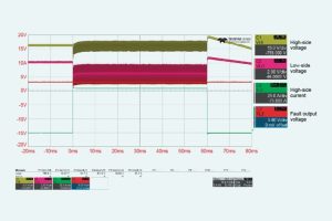
Figure 8: Oscilloscope screen capture – 4kW for 60ms. In lab tests the BCM6135 has demonstrated peak Power of 4kW (80A at 50V) for 60ms, an indicator that the module design is thermally robust across dynamic loads.
In a second lab test (Figure 9), the load was pulsed from 16A to 80A with a 10% duty cycle (900ms at 16A and 100ms at 80A). The operating condition is 520VHI and 32.5VLO; this is the low end of the supported BCM6135 voltage range. The average power delivery was 720W (22A at 32.5V). Over the course of 30 minutes (1800s), the internal sensor “read temperature” (a proxy for junction temperature) indicated a steady-state temperature of ~100°C, considerably below the maximum allowable junction temperature of 125°C. The test setup was passive cooling with a single-sided heat sink. This is another positive indicator for the targeted passively cooled application.
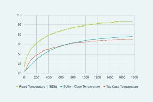
Figure 9: 10% duty cycle 16A to 80A load step with 100°C steady-state read temperature after 1800 seconds (with single-sided heat sink).
On the other hand, in a third lab test (see Figure 10), with the same thermal management setup, the average power delivery was increased to 1.1kW (22A at 50V). In this test, the operating condition is 800VHI and 50VLO; this is the high end of the supported BCM6135 voltage range. The load was pulsed from 17.5A to 70A with a 10% duty cycle (900ms at 17.5A and 100ms at 70A). In 7.5 minutes, the sensed internal temperature was 100°C and was still rising (not in steady state). But 7.5 minutes (450 seconds) is a much longer duration than 20 seconds, so this is a positive indicator that the BCM6135 may meet some active suspension design requirements.
Ultimately, the BCM6135 was lab characterized to support an average power of 1.3kW for 30 seconds with a passively-cooled heat sink across the sealed-enclosure operating temperature range.
Active suspension design objectives include road surface profile assumptions (amplitude and duration of bumps and holes that can be mitigated), and these assumptions bear directly on the required peak power capability of the DC-DC converter. The electromagnetic characteristics of the linear motor also impact the DC-DC converter requirements. That said, the BCM6135 is an indispensable bus converter module for contemporary active suspension, active anti-roll control DC-DC converter subsystems.
Conclusion
The economic and quality-of-life benefits of electrification is driving the adoption of HV to 48V DC-DC conversion across equipment types throughout the global economy. Integrated high-voltage to 48V power modules are becoming more common in EVs and HEVs as battery voltages increase and 48V low voltage buses become more widespread.
Next-generation bidirectional fixed-ratio bus converter modules are capable of meeting electrically and thermally demanding requirements in transient regenerative use case applications such as active electric vehicle suspensions. The passively cooled findings presented are significant in light of the accelerating trend towards more costly liquid-cooled power delivery systems.
The post High-voltage bus converter power modules for electric vehicle 48V power delivery networks appeared first on ELE Times.
Міжнародне співробітництво упродовж десятиліть між Україною та Польщею: власний досвід

18 червня в університеті відбулося нагородження Золотими почесними знаками Національної технічної організації – Федерації науково-технічних товариств Польщі.
Microchip Enhances TrustMANAGER Platform to Support CRA Compliance and Cybersecurity Regulations
International cybersecurity regulations continue to adapt to meet the evolving threat landscape. One major focus is on outdated firmware in IoT devices, which can present significant security vulnerabilities. To address these challenges, Microchip Technology is enhancing its TrustMANAGER platform to include secure code signing and Firmware Over-the-Air (FOTA) update delivery as well as remote management of firmware images, cryptographic keys and digital certificates. These advancements support compliance with the European Cyber Resilience Act (CRA) which mandates strong cybersecurity measures for digital products sold in the European Union (EU). Aligned with standards like the European Telecommunications Standards Institute (ETSI) EN 303 645 baseline requirements of cybersecurity for consumer IoT and the International Society of Automation (ISA)/International Electrotechnical Commission (IEC) 62443 security of industrial automation and control systems standards, the CRA sets a precedent that is expected to influence regulations worldwide.
Microchip’s ECC608 TrustMANAGER leverages Kudelski IoT’s keySTREAM Software as a Service (SaaS) to deliver a secure authentication Integrated Circuit (IC) that is designed to store, protect and manage cryptographic keys and certificates. With the addition of FOTA services, the platform helps customers securely deploy real-time firmware updates to remotely patch vulnerabilities and comply with cybersecurity regulations.
“As evolving cybersecurity regulations require connected device manufacturers to prioritize the implementation of mechanisms for secure firmware updates, lifecycle credential management and effective fleet deployment,” said Nuri Dagdeviren, corporate vice president of Microchip’s security products business unit. “The addition of FOTA services to Microchip’s TrustMANAGER platform offers a scalable solution that removes the need for manual, and expensive, static infrastructure security updates. FOTA updates allow customers to save resources while fulfilling compliance requirements and helping to future-proof their products against emerging threats and evolving regulations.”
Further enhancing cybersecurity compliance, the Microchip WINCS02PC Wi-Fi network controller module used in the TrustMANAGER development kit is now certified against the Radio Equipment Directive (RED) for secure and reliable cloud connectivity. RED establishes strict standards for radio devices in the EU, focusing on network security, data protection and fraud prevention. Beginning August 1, 2025, all wireless devices sold in the EU market must adhere to RED cybersecurity provisions.
By incorporating these additional services, TrustMANAGER—governed by keySTREAM—tackles key challenges with IoT security, regulatory compliance, device lifecycle management and fleet management. This solution is designed to serve IoT device manufacturers and industrial automation providers.
Development Tools
The ECC608 TrustMANAGER is compatible with the MPLAB X Integrated Development Environment (IDE) and supported by Microchip’s CryptoAuth PRO development board (EV89U05A) and the CryptoAuthLib software library. The Trust Platform Design Suite (TPDS) contains a use case example including onboarding educational steps and a firmware code example to enable the keySTREAM service to AWS with the ECC608 secure element running on a 32-bit Arm Cortex-M4-based PIC32CX SG41MCU and a WINCS02PC Wi-Fi module.
The post Microchip Enhances TrustMANAGER Platform to Support CRA Compliance and Cybersecurity Regulations appeared first on ELE Times.
EEVblog 1692 - $130 Fluke 17B MAX Multimeter REVIEW
Farads
 | submitted by /u/Linker3000 [link] [comments] |
Take back half improves PWM integral linearity and settling time

PWM is a simple, cool, cheap, cheerful, and (therefore) popular DAC technology. Excellent differential nonlinearity (DNL) and monotonicity are virtually guaranteed by PWM. Also guaranteed are a stable zero and a full-scale accuracy that’s generally limited only by the quality of the voltage reference. However, PWM’s integral nonlinearity (INL) isn’t always terrific, and the necessity for low-pass filtering-out of ripple means its speed isn’t too swift either. These messy topics are covered in…
- A common cause of, and a software cure for, PWM INL is discussed here in “Minimizing passive PWM ripple filter output impedance: How low can you go?”
- The slow PWM settling times (Ts) that can be problematic, together with a way to reduce them, are addressed here in “Cancel PWM DAC ripple with analog subtraction.”
Figure 1 offers a tricky, totally analog strategy for both. The ploy in play is Take Back Half (TBH). It relies on two differential relationships that effectively subtract (take back) the error terms.
- For signal frequencies less than or equal to 1/Ts (including DC) Xc >> R and Z = 2(Xavg – Yavg/2).
- For frequencies greater than or equal to Fpwm, Xc << R and Z = Xripple – Yripple.

Figure 1 All Rs and Cs are nominally equal. The circuit relies on two differential relationships that effectively subtract the error terms for the TBH methodology.
Wow the engineering world with your unique design: Design Ideas Submission Guide
Because only one switch drives load R at node Y while two in parallel drive X, INL due to switch loading at Y is exactly twice that at X. Therefore, Z = 2(Xavg – Yavg/2) takes back, cancels the error, and has (theoretically) zero INL.
Xripple = Yripple, so Z = Xripple – Yripple = 0 nulls it out, has likewise (theoretically) zero ripple, and ripple filter RC time constants can be made faster and settling times shorter.
The DC conversion component at Z = -PWM_duty_factor * Vref. Conversion accuracy is precisely unity, independent of resistance and capacitance tolerances. However, they ideally should be accurately equal for best ripple and nonlinearity cancellation.
Stephen Woodward’s relationship with EDN’s DI column goes back quite a long way. Over 100 submissions have been accepted since his first contribution back in 1974.
Related Content
- Minimizing passive PWM ripple filter output impedance: How low can you go?
- Cancel PWM DAC ripple with analog subtraction
- Temperature controller has “take-back-half” convergence algorithm
- 20MHz VFC with take-back-half charge pump
- Take-Back-Half precision diode charge pump
The post Take back half improves PWM integral linearity and settling time appeared first on EDN.
ELENA project develops Europe’s first LNOI substrates for photonic integrated circuits, completing supply chain
Засідання Наглядової ради проєкту «Коаліція укриттів цивільного захисту»

На заході обговорювалися подальші кроки щодо розвитку мережі укриттів по всій території України і були присутні представники України та Фінляндії:
Сторінки

