
Збирач потоків
Vishay Intertechnology’s 1200 V SiC MOSFET Power Modules for Power Efficiency
Vishay Intertechnology, Inc. has introduced five new 1200 V MOSFET power modules designed to increase power efficiency for medium to high frequency applications in automotive, energy, industrial, and telecom systems. The Vishay Semiconductors VS-SF50LA120, VS-SF50SA120, VS-SF100SA120, VS-SF150SA120, and VS-SF200SA120 feature Vishay’s latest generation silicon carbide (SiC) MOSFETs in the industry-standard SOT-227 package.
Offered in single switch and low side chopper configurations, each power module released today features a SiC MOSFET integrated with a soft body diode offering low reverse recovery. The result is reduced switching losses and increased efficiency for solar inverters, off-board chargers for electric vehicles (EV), SMPS, DC/DC converters, UPS, and HVAC systems; large-scale battery storage systems, and telecom power supplies.
The compact SOT-227 package of the VS-SF50LA120, VS-SF50SA120, VS-SF100SA120, VS-SF150SA120, and VS-SF200SA120 allows the devices to serve as drop-in replacements for competing solutions in existing designs, enabling designers to adopt one of the newest SiC technologies without the expense of changing PCB layouts. The moulded package also offers electrical insulation up to 2500 V for one minute, lowering costs by eliminating the need for additional insulation between the component and heatsink.
The power modules provide continuous drain current from 50 A to 200 A and low on-resistance down to 12.1 mΩ. The RoHS-compliant devices deliver high-speed switching with low capacitance and offer a high maximum operating junction temperature of +175 °C.
Device Specification Table:
|
Part # |
VDSS |
ID |
RDS(ON) |
Configuration |
Package |
|
VS-SF50LA120 |
1200 V |
50 A |
43 mΩ |
Low side chopper |
SOT-227 |
|
VS-SF50SA120 |
50 A |
47 mΩ |
Single switch |
||
|
VS-SF100SA120 |
100 A |
23 mΩ |
Single switch |
||
|
VS-SF150SA120 |
150 A |
16.8 mΩ |
Single switch |
||
|
VS-SF200SA120 |
200 A |
12.1 mΩ |
Single switch |
Samples and production quantities of the VS-SF50LA120, VS-SF50SA120, VS-SF100SA120, VS-SF150SA120, and VS-SF200SA120 are available now, with lead times of 13 weeks.
The post Vishay Intertechnology’s 1200 V SiC MOSFET Power Modules for Power Efficiency appeared first on ELE Times.
Budget 2026-27: Can New PLI Schemes Drive India’s A&D Tech Sovereignty?
As the Union Budget approaches, the spotlight intensifies on India’s aerospace and defence technology sector, a vertical that has transitioned from a heavy importer to a nascent global manufacturing hub. The numbers tell a story of aggressive scaling: under the aegis of “Atmanirbhar Bharat,” domestic defence production surged to a historic ₹1.27 lakh crore in FY 2023-24.
However, for an industry eyeing a $5 trillion economy, this record high is viewed not as a finish line, but as a baseline. The shift toward indigenous manufacturing has fundamentally rewired the nation’s military-industrial complex, replacing foreign dependency with homegrown R&D and high-tech sovereignty. As the government prepares to lay out its fiscal roadmap, the industry is looking for more than just procurement orders; it is looking for deep-tech incentives, streamlined export pathways, and sustained capital outlay.
This budget will be a litmus test for India’s self-reliance commitment. Stakeholders are bracing for announcements that could further catalyse the aerospace ecosystem, ensuring that “Made in India” weaponry and avionics don’t just meet internal security needs but become a cornerstone of India’s global economic footprint.
The Tech-Sovereignty Mandate
As the lines between commercial innovation and battlefield superiority blur, technology has emerged as the definitive fulcrum for India’s tri-service modernisation. Industry experts argue that the upcoming Budget presents a pivotal window to institutionalise this convergence through aggressive structural reforms.
Central to this discourse is the evolution of the Production Linked Incentive (PLI) Scheme. While the current framework has provided a vital tailwind for the drone industry, there is a growing consensus that a “narrow-lens” approach is no longer sufficient. To truly insulate India’s supply chain from global volatility, the PLI umbrella must expand to cover the high-stakes world of dual-use technologies.
In terms of using technology in aerospace and defence technology development, the use of AI and related features will play a significant role.
“Investing in digital twins and simulation technology for testing and research in aviation and defence can boost precision and efficiency in the electronic manufacturing industry. Tecknotrove urges the government to prioritize use of digital twin technology in this financial budget. It’s a strategic move that will amplify innovation, save research and development and manufacturing costs, and drive India’s self-reliance in manufacturing. Digital twins aren’t just a trend—they’re a game-changer. With decades of expertise in digital twins for aviation and defence, we have seen this technology helping in at least 30% reduction in costs,” says Payal Gupta, Co-Founder, Director-Business Development, Tecknotrove Systems India Pvt. Ltd.
The strategic roadmap for the FY 2026-27 fiscal cycle should ideally prioritise:
- The Full Drone Spectrum: Moving beyond basic assembly to incentivise the manufacturing of high-endurance propulsion systems and autonomous flight controllers.
- Electronic Warfare & Surveillance: Bringing Airborne Early Warning (AEW) systems, jamming devices, and advanced radar arrays under the incentive net to neutralise import dependencies.
- The Robotics Frontier: Providing fiscal stimulus for indigenous sensors and robotic systems that will define the future of unmanned combat and deep-space communication.
By widening these incentive corridors, the government can transform the “Make in India” initiative from a manufacturing slogan into a high-tech powerhouse, ensuring that the next generation of aerospace sensors and AI-driven robotics are conceived, designed, and built on Indian soil.
By: Shreya Bansal, Sub-Editor
The post Budget 2026-27: Can New PLI Schemes Drive India’s A&D Tech Sovereignty? appeared first on ELE Times.
How to Build a Hacker-Proof Car: Insights from the Auto EV Tech Summit
Speaking at the Auto EV Tech Vision Summit 2025, Suresh D highlights the major cyber vulnerabilities and the corresponding technologies required to enable a safer and more resilient automotive ecosystem.
Since the electronic components in passenger vehicles are set to increase by 20-40 percent, as the recent studies suggest, including infotainment, ADAS, etc, drawing in a lot of sensors in the near future, automobiles are emerging as the new battlefield for cyber developments. Underlining this growing phenomenon, Suresh D, Group CTO, Minda Corporation, CEO, Spark Minda Tech Centre & Board Member, Spark Minda Green Mobility says, “A passenger vehicle is expected to see a 20–40 percent increase—nearly doubling in some cases—over the next two to three years, bringing in a large number of on-board electronic systems. This will significantly increase software content and complexity,” at the Auto EV Tech Vision Summit 2025 held at KTPO, Bengaluru, on November 18–19, 2025.
He further goes on to add that the phenomenon will make Operating Systems and other software indispensable, escalating the security question in automobiles.
Critical Challenges on the way
He says that the new architectural parameter of SDVs, where the distributed architecture is being replaced by controlled or zonal architecture, also poses certain security challenges. Also, as the new vehicles remain entirely connected, as in V-2-V or V-2-I connection, the proximity of cyber risks escalates.
Further, he touches upon the critical challenges that are to be tackled, including phishing, hacking, snooping, malware, etc. He goes on to underline some of the crucial cyberattacks that the automotive industry has seen in the recent past, ranging from CAN spoofing a Jeep Cherokee in 2014 to the latest TESLAMATE attack on Tesla cars in 2025, underlining how the question of cybersecurity becomes more relevant than ever.
Curious Case of SDVs & EVs
As EVs are on the rise across the world, Suresh D highlights how EV expansion and the need for robust charging systems also aggravate the risk. He explains that if a charging station compromises a supplier’s build server, it can be manipulated to tamper with BMS parameters via a compromised internal bus or a malicious charging station.
While for SDVs, potential risk sources he underlines include attack scenarios ranging from unprivileged root access and pivoting through fleet management backends, to compromised third-party apps and poorly protected cryptographic keys.
How to Tackle this?
In the latter part, he touches upon the important steps that can be taken to avoid the potential risks and create a safer and reliable cyber ecosystem for automotives. First among them is the System Architecture approach. He says, “It refers to developing a robust architecture—understanding the OEM’s architecture and aligning the product accordingly.” He sums it up as thinking way ahead of the OEMs. It also includes encryption and decryption of the hardware to ensure that no vulnerability remains open to exploitation.
Further, he also outlines a distinct approach, which is Embedded Edge Solutions, which means solving the problem at the source. It includes several protections, including secure flashing and secure boot. This is done through the plant server of the OEM that generates distinct private keys for each of the units for further authorization.
For SDVs, he highlights a telematics-based approach which consists of 3 layers, namely Layer 1- In-vehicle security, Layer 2- Vehicle Communication Security & Layer 3- The cloud infrastructure. When Internet Protocol is used for communication, it enables whitelisting of the IPs through encryption and decryption through SSL, enabling a better and safer environment.
High Frequency Options: Granting More Immunity
He also underlines how automobiles these days usually come with smart keys or keyless access to the vehicle. While the technology is referred to as Low-Frequency Radio Frequency (LFRF), it is immune to relay attacks. However, the industry is gradually moving towards safer and more reliable options like Bluetooth and Ultra Wide Bandgap (UWB), with high-frequency technology making decoding highly difficult.
He adds that even these technologies are prone to cyberattacks, either at the server level or the device level. Conclusively, some techniques like channel sounding with Bluetooth-based technology have been developed, which are more precise and help make authentication more secure. It offers a turnkey secure foundation, making automobiles reliable and secure.
The post How to Build a Hacker-Proof Car: Insights from the Auto EV Tech Summit appeared first on ELE Times.
Palo Alto Networks Unifies Observability and Security for the AI Era through Chronosphere Acquisition
As enterprises increasingly rely on AI to run digital operations, protect assets, and drive growth, success depends on one critical factor: trusted, high-quality, real-time data. Palo Alto Networks, the global cybersecurity leader, announced the completion of its acquisition of Chronosphere, addressing a core challenge of the AI era: the inability to see and secure the massive data volumes running modern businesses.
Chronosphere, a Leader in the 2025 Gartner Magic Quadrant for Observability Platforms, was purpose-built to handle this scale. While legacy tools break down in cloud-native environments, Chronosphere gives customers deep visibility across their entire digital estate. With this acquisition, Palo Alto Networks is redefining how organisations run at the speed of AI—by enabling customers to gain deep, real-time visibility into their applications, infrastructure, and AI systems — while maintaining strict control over data cost and value.
The planned integration of Palo Alto Networks Cortex AgentiX with Chronosphere’s cloud-native observability platform will allow customers to apply AI agents that can now find and fix security and IT issues automatically—before they impact the customer or the bottom line. AI security without deep observability is blind; this acquisition delivers the essential context across models, prompts, users, and performance to move from manual guessing to autonomous remediation.
Nikesh Arora, Chairman and CEO, Palo Alto Networks:
“Enterprises today are looking for fewer vendors, deeper partnerships, and platforms they can rely on for mission-critical security and operations. Chronosphere accelerates our vision to be the indispensable platform for securing and operating the cloud and AI. We believe that great security starts with deep visibility into all your data, and Chronosphere provides that foundation for our customers.”
Martin Mao, Co-founder and CEO, Chronosphere, is joining Palo Alto Networks as SVP, GM Observability and comments:
“Chronosphere was built to help the world’s most complex digital organisations operate at scale with confidence. Joining Palo Alto Networks allows us to bring AI-era observability to a global audience. Together, we’re delivering a new standard — where observability, security, and AI come together to give organisations control over their most valuable asset: data.”
The Chronosphere Telemetry Pipeline remains available as a standalone solution, enabling organisations to eliminate the ‘data tax’ associated with modern security operations. By acting as an intelligent control layer, the pipeline filters low-value noise to reduce data volumes by 30% or more while requiring 20x less infrastructure than legacy alternatives. This is key to Palo Alto Networks Cortex XSIAM strategy, ensuring customers can scale their security posture—not their spending—as they transition to autonomous, AI-driven operations.
The post Palo Alto Networks Unifies Observability and Security for the AI Era through Chronosphere Acquisition appeared first on ELE Times.
EEVblog 1732 - 20yo 1000+ Cycle Panasonic Li-Ion Battery TESTED
Учений КПІ Юрій Яворський — лауреат премії Верховної Ради України

Доцент кафедри фізичного матеріалознавства та термічної обробки (ФМТО) Інституту матеріалознавства та зварювання ім. Є. О. Патона (ІМЗ) Юрій Яворський отримав Премію Верховної Ради України молодим ученим — одну з найпрестижніших державних відзнак для молодих науковців.
КПІ та КНДІСЕ посилюють співпрацю у сфері судових експертиз

КПІ ім. Ігоря Сікорського та Київський науково-дослідний інститут судових експертиз (КНДІСЕ) провели робочу зустріч, щоб посилити партнерство та вивести наукову й освітню співпрацю на новий стратегічний рівень.
Wolfspeed unveils TOLT package portfolio
NEC develops high-efficiency compact power amplifier module for sub-6GHz band in 5G base-station radio units
Vishay launches 1200V SiC MOSFET power modules in SOT-227 packages
Spectral Engineering and Control Architectures Powering Human-Centric LED Lighting
As technological advancements continue to pursue personalisation & customisation at every level, illumination has also transformed from a need to a customisation. Consequently, the LED industry is moving towards a similar yet prominent stride, making customised and occasion-specific solutions, keeping in consideration the human behaviour and lighting changes across the day. Long seen as the constant and uniform thing, illumination is now being reimagined as something dynamic and customisable.
In the same pursuit, the industry has moved towards enabling Human-Centric Lighting(HCL), where lighting is designed and engineered to emulate natural daylight, ranging from dimming them as the Sun goes down, while brightening up as the day begins. Gradually, illumination is now being designed around human biology, visual comfort, and cognitive performance rather than simple brightness or energy efficiency.
But what lies behind this marvel is hardcore engineering. Technically, the result is made possible by the marvels of spectral engineering & control architectures, wherein the former adjusts the light spectrum while the latter enables the intelligence directing the timing changes of the lighting system. Simultaneously, the dual play brings forth today’s human-centric lighting into real-life examples and is also making them more customised and personalised. This ultimately helps in supporting human circadian rhythms, enhancing well-being, mood, and performance.
To enable these engineered outcomes, embedded sensors, digital drivers, and networked control platforms are integrated into the modern-day LED lights, transforming illumination into a responsive, data-driven infrastructure layer. In combination, spectral engineering and intelligent control systems are reshaping the capabilities of LED lighting, transforming it from a passive utility into a dynamic, precision-engineered tool for enhancing human wellbeing, productivity, and performance.
How is Spectral Power Distribution engineered?
When we talk about LED lights, white light is the first thing that comes to our minds. Although the same is not true scientifically. Surprisingly, LEDs inherently emit blue light and not white. To turn the blue light into white, a Phosphor coating is applied over it. Consequently, the blue light mixes with the phosphor to turn some of the light into green, red & yellow simultaneously. These lights eventually mix to turn white.
Spectral Power Distribution (SPD) is simply the profile of the white colour which is not visible to our naked eyes, and how much of each colour is present in the visible white light. The final light can be controlled by various means, such as the type of phosphor, how thick the phosphor layer is, or by adding extra coloured LEDs (like red or cyan).
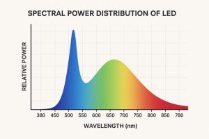
Spectral Power Distribution is engineered by carefully mixing different colours of light inside an LED, even though it looks white, so that the light feels right for the human body and mind.
Engineering the Spectral Power Distribution of White LEDs
Often, it is seen that the very same white light is sometimes harsh while sometimes soft- all this is because of various variables. Today, from being a static character, SPD has turned into a tunable design parameter,++ becoming a Controllable Design Variable. To this effect, SPD is largely controlled by Phosphor composition (which colours it emits), Particle size and density, and finally Layer thickness and distribution.
That’s why the same 400K LEDs from different manufacturers can feel completely different — their SPDs are different, even if the Correlated Color Temperature (CCT) is the same. But as long as the final color is decided by some application made during manufacturing, the effect remains static. While spectral Power distribution is essential, it is equally important to dictate the given behaviour as per the time of the day.
Multi-Channel LED Configurations for Spectral Tunability
To enable a real-time nature to this Spectral tunability, engineers today use multiple LED channels, including:
- White + Red
- White + Cyan
- RGBW / RGBA
- Tunable white (warm white + cool white)
By precisely varying the current supplied to each LED channel, the spectral power distribution can be reshaped in real time, allowing the system to shift between blue-enriched and blue-reduced lighting modes as required. This level of control allows you to adjust the perceived colour temperature independently of the light’s biological impact, rather than having them locked together. As a result, SPD is no longer a fixed characteristic of the light source but becomes a dynamic, real-time controllable design parameter.
Melanopic Response, Circadian Metrics, and Spectral Weighting
When we talk about light, visibility & brightness make up the primary issue, but that has changed drastically with the emergence of Human Centric Lighting (HCL). With HCL coming into play, photopic lux, the quantification of brightness, is no longer a go-to metric to decide upon the quality of lighting. It is because it explained only one part of the coin, which is visibility, and not how this light or visibility affects human biology.
At the same time, Human Centered Lighting focuses on how light affects the circadian system, alertness, sleep–wake cycles, mood, and hormonal regulation. This phenomenon has brought up new metrics that tell us not only about the brightness or visibility, but also how it biologically acts. One such metric is Melanopic Lux, which weights the spectrum based on melanopsin sensitivity. Melanopsin is a photopigment in our eyes, usually sensitive to Blue-Cyan light.
Interestingly, more melanopic stimulation → increased alertness and circadian activation, while less melanopic stimulation → relaxation and readiness for sleep. That’s where we come to the core of our subject – Light induced behaviuour. The emergence of Melanopic Lux allows engineers to decouple visual brightness from biological effect, giving the right direction to Human Centric Lighting.
While melanopic metrics define what kind of biological response light should produce, control architectures determine when and how that response is delivered. Translating circadian intent into real-world lighting behaviour requires intelligent control systems capable of dynamically adjusting spectrum, intensity, and timing throughout the day. This is where embedded sensors, digital LED drivers, and networked control platforms come into play, enabling lighting systems to modulate melanopic content in real time—boosting circadian stimulation during the day and reducing it in the evening—without compromising visual comfort or energy efficiency.
Other metrics, such as Melanopic Equivalent Daylight Illuminance (EDI) and Circadian Stimulus (CS) are used to quantify how effectively a light source supports circadian activation or melatonin suppression, beyond what photopic lux can describe.
LED Drivers and Power Electronics for Dynamic Spectral Control
In human-centric lighting systems, LED drivers are no longer simple power supplies but precision control elements that translate circadian intent into real-world illumination. Because LEDs are current-driven devices, accurate current regulation is essential to maintain stable brightness and spectral output, especially as temperature and operating conditions change.

Dynamic spectral tuning typically relies on multi-channel LED architectures, making channel balancing a critical requirement. Each LED colour behaves differently electrically and thermally, and without independent, well-balanced current control, the intended spectral profile can drift over time, affecting both visual quality and biological impact.
Equally important is dimming accuracy. Human-centric lighting demands smooth, flicker-free dimming that preserves spectral integrity at all brightness levels, particularly during low-light, evening scenarios. Advanced driver designs enable fine-grained dimming and seamless transitions, allowing lighting systems to dynamically adjust spectrum and intensity throughout the day while maintaining visual comfort and circadian alignment.
System Integration Challenges and Design Trade-Offs
While human-centric lighting promises precise control over both visual and biological responses, delivering this in real-world systems involves significant integration challenges and design trade-offs. Spectral accuracy, electrical efficiency, thermal management, and system cost must all be balanced within tight form-factor and reliability constraints. Multi-channel LED engines increase optical and control complexity, while higher channel counts demand more sophisticated drivers, sensing, and calibration strategies.
Thermal effects further complicate integration, as LED junction temperature directly influences efficiency, colour stability, and lifetime. Without careful thermal design and feedback control, even well-engineered spectral profiles can drift over time. At the same time, adding sensors, networking, and intelligence introduces latency, interoperability, and cybersecurity considerations that must be addressed at the system level.
Ultimately, successful human-centric lighting solutions are defined not by any single component, but by holistic co-design—where optics, power electronics, controls, and circadian metrics are engineered together. The trade-offs made at each layer determine whether a system merely adjusts colour temperature or truly delivers biologically meaningful, reliable, and scalable lighting performance.
The post Spectral Engineering and Control Architectures Powering Human-Centric LED Lighting appeared first on ELE Times.
Dell Technologies Enables NxtGen to Build India’s Largest AI Factory
Story Highlights
Dell AI Factory with NVIDIA to provide scalable and secure infrastructure for NxtGen’s AI platform, India’s first and largest AI factory, enabling national-scale AI development.
This milestone deployment accelerates India’s AI mission, enabling large‑scale generative, agentic, and physical AI while expanding NxtGen’s high‑performance AI services nationwide.
Dell Technologies today announced that NxtGen AI Pvt Ltd, one of India’s foremost sovereign cloud and AI infrastructure providers, has selected Dell AI Factory with NVIDIA solutions for building India’s first and largest dedicated AI factory. This milestone deployment will significantly expand India’s national AI capability, enabling large-scale generative AI, agentic AI, physical AI, and high-performance computing across enterprises, start-ups, and government programs.
Dell will provide the core infrastructure, including Vertiv liquid-cooled Dell PowerEdge XE9685L servers, delivered through Dell Integrated Rack Scalable Systems, for NxtGen’s new AI cluster, empowering the company to meet the growing demand for AI as a Service and large-scale GPU capacity.
Why it matters
This accelerated computing infrastructure is vital for advancing India’s AI mission, significantly expanding NxtGen’s AI cloud services for a diverse range of clients, from start-ups to academia and government. By empowering NxtGen with this advanced foundation, Dell is accelerating India’s next wave of AI development and innovation, ensuring critical access to high-performance AI capabilities across the region.
Powering the future of AI with advanced Dell AI infrastructure
The Dell AI Factory with NVIDIA combines AI infrastructure, software, and services in an advanced, full-stack platform designed to meet the most demanding AI workloads and deliver scalable, reliable performance for training and inference. Leveraging the Dell AI Factory with NVIDIA, NxtGen will deploy Vertiv liquid-cooled, fully integrated Dell IR5000 racks featuring Dell PowerEdge XE9685L servers with the NVIDIA accelerated computing platform to build a cluster with over 4,000 NVIDIA Blackwell GPUs, NVIDIA BlueField-3 DPUs, and NVIDIA Spectrum-X Ethernet networking, all purpose-built for AI. These will be complemented by Dell PowerEdge R670 servers and Dell PowerScale F710 storage.
Dell AI Factory with NVIDIA: Empowering AI for Human Progress
The Dell AI Factory with NVIDIA offers a full stack of AI solutions from data center to edge, enabling organizations to rapidly adopt and scale AI deployments. The integration of Dell’s AI capabilities with NVIDIA’s accelerated computing, networking, and software technologies provides customers with an extensive AI portfolio and an open ecosystem of technology partners. With more than 3,000 customers globally, the Dell AI Factory with NVIDIA reflects Dell’s leadership in enabling enterprises with scalable, secure and high-performance AI infrastructure.
The comprehensive Dell AI Factory with NVIDIA portfolio provides a simplified and reliable foundation for NxtGen to deliver advanced AI capabilities at speed and scale. This allows NxtGen to deliver on its core mission of providing sovereign, cost-effective and powerful AI services that help businesses grow and innovate, while at the same time reinforcing Dell’s commitment to providing the technology that drives human progress.
By equipping organizations like NxtGen with cutting-edge AI infrastructure and services, Dell is helping to unlock new possibilities and create a future where technology empowers everyone to achieve more.
Perspectives
“India’s rapid AI growth demands strong, reliable, and future-ready infrastructure,” said Manish Gupta, president and managing director, India, Dell Technologies. “Dell Technologies is addressing this need through the Dell AI Factory with NVIDIA, designed to simplify and scale AI deployments across industries. As the top AI infrastructure provider, we are enabling this shift by combining storage, compute, networking and software to accelerate AI adoption. Our collaboration with NxtGen brings these capabilities closer to Indian enterprises, helping them deploy AI efficiently and cost-effectively. This marks another step in our commitment to empowering India’s digital future through secure, scalable, and sovereign AI infrastructure.”
“NxtGen is committed to building India’s AI backbone,” said A. S. Rajgopal, managing director and chief executive officer, NxtGen. “This deployment marks a significant milestone for the country: India’s largest AI model-training cluster, built and operated entirely within India’s sovereign cloud framework. Dell Technologies has been critical in enabling this scale, performance, and reliability. Together, we are unlocking the infrastructure that will power the next generation of Indian AI models and applications.”
“India’s ambitious AI mission requires a foundation of secure, high-performance accelerated computing infrastructure to enable model and AI application development,” said Vishal Dhupar, managing director, Asia South, NVIDIA. “Dell’s integration of NVIDIA AI software and infrastructure, including NVIDIA Blackwell GPUs and NVIDIA Spectrum-X networking, provides the AI factory resources to help NxtGen accelerate this critical national capability.”
The post Dell Technologies Enables NxtGen to Build India’s Largest AI Factory appeared first on ELE Times.
Quest Global Appoints Richard Bergman as Global Business Head of its Semiconductor Division
Bengaluru, India, January 28th, 2026 – Quest Global, the world’s largest independent pure-play engineering services company, today announced the appointment of Richard (Rick) Bergman as President & Global Business Head of its Semiconductor vertical.
As the Global Business Head, Rick will focus on shaping the division’s long-term strategy, accelerating revenue growth, and deepening relationships with global customers. His responsibilities include defining a multi-year growth roadmap, supporting clients’ success through high-impact and transformational solutions, especially in AI, automotive, and industrial sectors, and fostering a culture of innovation and operational excellence to meet next-generation engineering demands.
“The semiconductor industry is at a turning point, fueled by AI, system innovation, and shifting supply chains,” says Ajit Prabhu, Co-Founder and CEO, Quest Global. “Rick is a fantastic addition to our team. He brings incredible leadership across semiconductors and computing, plus a real talent for scaling organizations and building genuine, long-term relationships with customers. Bringing him on board is a clear sign of our commitment to growing this vertical and making sure Quest Global remains a humble, trusted partner for engineering and transformation in this space.”
“Semiconductors are the foundational enablers of innovation across AI, high-performance computing, automotive, communications, and industrial systems,” said Rick Bergman, President & Global Business Head – Semiconductor, Quest Global. “What attracted me to Quest Global is the company’s unique combination of deep engineering DNA, global scale, and a long-term partnership mindset with customers. As the industry navigates increasing complexity, my focus will be on helping customers solve their most critical engineering challenges while building a scalable, high-impact business.”
Rick brings more than two decades of leadership experience across semiconductors, computing, graphics, and advanced technology platforms. Most recently, he served as President and CEO of Kymeta Corporation. Previously, he held senior leadership roles at AMD, Synaptics, and ATI Technologies. Throughout his career, Rick has led multi-billion-dollar businesses, overseen major acquisitions, and built high-performing global teams.
This appointment underscores Quest Global’s commitment to building category-leading leadership and scaling its Semiconductor business, aligned with evolving customer needs.
About Quest Global
At Quest Global, it’s not just what we do but how and why we do it that makes us different. We’re in the business of engineering, but what we’re really creating is a brighter future. For over 25 years, we’ve been solving the world’s most complex engineering problems. Operating in over 18 countries, with over 93 global delivery centers, our 21,500+ curious minds embrace the power of doing things differently to make the impossible possible. Using a multi-dimensional approach, combining technology, industry expertise, and diverse talents, we tackle critical challenges faster and more effectively. And we do it across the Aerospace & Defense, Automotive, Energy, Hi-Tech, MedTech & Healthcare, Rail and Semiconductor industries. For world-class end-to-end engineering solutions, we are your trusted partner.
The post Quest Global Appoints Richard Bergman as Global Business Head of its Semiconductor Division appeared first on ELE Times.
VIS licenses TSMC’s 650V and 80V GaN technology
Round pegs, square holes: Why GPGPUs are an architectural mismatch for modern LLMs

The saying “round pegs do not fit square holes” persists because it captures a deep engineering reality: inefficiency most often arises not from flawed components, but from misalignment between a system’s assumptions and the problem it is asked to solve. A square hole is not poorly made; it’s simply optimized for square pegs.
Modern large language models (LLMs) now find themselves in exactly this situation. Although they are overwhelmingly executed on general-purpose graphics processing units (GPGPUs), these processors were never shaped around the needs of enormous inference-based matrix multiplications.
GPUs dominate not because they are a perfect match, but because they were already available, massively parallel, and economically scalable when deep learning began to grow, especially for training AI models.
What follows is not an indictment of GPUs, but a careful explanation of why they are extraordinarily effective when the workload is rather dynamic and unpredictable, such as graphic processing, and disappointedly inefficient when the workload is essentially regular and predictable, such as AI/LLM inference execution.
The inefficiencies that emerge are not accidental; they are structural, predictable, and increasingly expensive as models continue to evolve.
Execution geometry and the meaning of “square”
When a GPU renders a graphic scene, it deals with a workload that is considerably irregular at the macro level, but rather regular at the micro level. A graphic scene changes in real time with significant variations in content—changes in triangles and illumination—but in an image, there is usually a lot of local regularity.
One frame displays a simple brick wall, the next, an explosion creating thousands of tiny triangles and complex lighting changes. To handle this, the GPU architecture relies on a single-instruction multiple threads (SIMT) or wave/warp-based approach where all threads in a “wave” or “warp,” usually between 16 and 128, receive the same instruction at once.
This works rather efficiently for graphics because, while the whole scene is a mess, local patches of pixels are usually doing the same thing. This allows the GPU to be a “micro-manager,” constantly and dynamically scheduling these tiny waves to react to the scene’s chaos.
However, when applied to AI and LLMs, the workload changes entirely. AI processing is built on tensor math and matrix multiplication, which is fundamentally regular and predictable. Unlike a highly dynamic game scene, matrix math is just an immense but steady flow of numbers. Because AI is so consistent, the GPU’s fancy, high-speed micro-management becomes unnecessary. In this context, that hardware is just “overhead,” consuming power and space for a flexibility that the AI doesn’t actually use.
This leaves the GPGPU in a bit of a paradox: it’s simultaneously too dynamic and not dynamic enough. It’s too dynamic because it wastes energy on micro-level programming and complex scheduling that a steady AI workload doesn’t require. Yet it’s not dynamic enough because it is bound by the rigid size of its “waves.”
If the AI math doesn’t perfectly fit into a warp of 32, the GPU must use “padding,” effectively leaving seats empty on the bus. While the GPU is a perfect match for solving irregular graphics problems, it’s an imperfect fit for the sheer, repetitive scale of modern tensor processing.
Wasted area as a physical quantity
This inefficiency can be understood geometrically. A circle inscribed in a square leaves about 21% of the square’s area unused. In processing hardware terms, the “area” corresponds to execution lanes, cycles, bandwidth, and joules. Any portion of these resources that performs work that does not advance the model’s output is wasted area.
The utilization gap (MFU)
The primary way to quantify this inefficiency is through Model FLOPs Utilization (MFU). This metric measures how much of the chip’s theoretical peak math power is actually being used for the model’s calculations versus how much is wasted on overhead, data movement, or idling.
For an LLM like GPT-4 running on GPGPT-based accelerators operating in interactive mode, the MFU drops by an order of magnitude with the hardware busy with “bookkeeping,” which encompasses moving data between memory levels, managing thread synchronization, or waiting for the next “wave” of instructions to be decoded.
The energy cost of flexibility
The inefficiency is even more visible in power consumption. A significant portion of that energy is spent powering the “dynamic micromanagement,” namely, the logic gates that handle warp scheduling, branch prediction, and instruction fetching for irregular tasks.
The “padding” penalty
Finally, there is the “padding” inefficiency. Because a GPGPU-based accelerator operates in fixed wave sizes (typically 32 or 64 threads), if the specific calculation doesn’t perfectly align with those multiples, often happening in the “Attention” mechanism of the LLM model, the GPGPU still burns the power for a full wave while some threads sit idle.
These effects multiply rather than add. A GPU may be promoted with a high throughput, but once deployed, may deliver only a fraction of its peak useful throughput for LLM inference, while drawing close to peak power.
The memory wall and idle compute
Even if compute utilization was perfect, LLM inference would still collide with the memory wall, the growing disparity between how fast processors can compute and how fast they can access memory. LLM inference has low arithmetic intensity, meaning that relatively few floating-point operations are performed per byte of data fetched. Much of the execution time is spent reading and writing the key-value (KV) cache.
GPUs attempt to hide memory latency using massive concurrency. Each streaming multiprocessor (SM) holds many warps and switches between them while others wait for memory. This strategy works well when memory accesses are staggered and independent. In LLM inference, however, many warps stall simultaneously while waiting for similar memory accesses.
As a result, SMs spend large fractions of idle time, not because they lack instructions, but because data cannot arrive fast enough. Measurements commonly show that 50–70% of cycles during inference are lost to memory stalls. Importantly, the power draw does not scale down proportionally since clocks continue toggling and control logic remains active, resulting in poor energy efficiency.
Predictable stride assumptions and the cost of generality
To maximize bandwidth, GPUs rely on predictable stride assumptions; that is, the expectation that memory accesses follow regular patterns. This enables techniques such as cache line coalescing and memory swizzling, a remapping of addresses designed to avoid bank conflicts and improve locality.
LLM memory access patterns violate these assumptions. Accesses into the KV cache depend on token position, sequence length, and request interleaving across users. The result is reduced cache effectiveness and increased pressure on address-generation logic. The hardware expends additional cycles and energy rearranging data that cannot be reused.
This is often described as a “generality tax.”
Why GPUs still dominate
Given these inefficiencies, it’s natural to ask why GPUs remain dominant. The answer lies in history rather than optimality. Early deep learning workloads were dominated by dense linear algebra, which mapped reasonably well onto GPU hardware. Training budgets were large enough that inefficiency could be absorbed.
Inference changes priorities. Latency, cost per token, and energy efficiency now matter more than peak throughput. At this stage, structural inefficiencies are no longer abstract; they directly translate into operational cost.
From adapting models to aligning hardware
For years, the industry focused on adapting models to hardware such as larger batches, heavier padding, and more aggressive quantization. These techniques smooth the mismatch but do not remove it.
A growing alternative is architectural alignment: building hardware whose execution model matches the structure of LLMs themselves. Such designs schedule work around tokens rather than warps, and memory systems are optimized for KV locality instead of predictable strides. By eliminating unused execution lanes entirely, these systems reclaim the wasted area rather than hiding it.
The inefficiencies seen in modern AI data centers—idle compute, memory stalls, padding overhead, and excess power draw—are not signs of poor engineering. They are the inevitable result of forcing a smooth, temporal workload into a rigid, geometric execution model.
GPUs remain masterfully engineered square holes. LLMs remain inherently round pegs. As AI becomes a key ingredient in global infrastructure, the cost of this mismatch becomes the problem itself. The next phase of AI computing will belong not to those who shave the peg more cleverly, but to those who reshape the hole to match the true geometry of the workload.
Lauro Rizzatti is a business advisor to VSORA, a technology company offering silicon semiconductor solutions that redefine performance. He is a noted chip design verification consultant and industry expert on hardware emulation.
Special Section: AI Design
- The AI design world in 2026: What you need to know
- AI workloads demand smarter SoC interconnect design
- AI’s insatiable appetite for memory
- The AI-tuned DRAM solutions for edge AI workloads
- Designing edge AI for industrial applications
The post Round pegs, square holes: Why GPGPUs are an architectural mismatch for modern LLMs appeared first on EDN.
📰 Газета "Київський політехнік" № 3-4 за 2026 (.pdf)

Вийшов 3-4 номер газети "Київський політехнік" за 2026 рік
Def-Tech CON 2026: India’s Biggest Conference on Advanced Aerospace, Defence and Space Technologies to Take Place in Bengaluru.
The two-day international technology conference is focused on promoting innovation in the Aerospace, Defence, and Space sectors, in conjunction with DEF-TECH Bharat 2026, held in Bengaluru.
With a strong India-centric focus, DefTech CON 2026 features high-impact keynote sessions, expert panels, technology showcases, and interactive QA sessions, covering areas such as AI & autonomous systems, cyber defence, unmanned systems, advanced materials, space tech, next-generation battlefield solutions, advanced sensors, secure communication networks, AI-driven command and control, electronic warfare systems, autonomous platforms, space-based surveillance, next-generation missile defence, and more. These technologies enable faster decision-making, enhanced interoperability, and greater operational dominance across land, air, sea, cyber, and space.
Designed as a venue for engineers, researchers, defence laboratories, industry leaders, startups, and system integrators, the conference unites India’s most brilliant minds to investigate emerging trends, groundbreaking solutions, and essential capabilities that are influencing the strategic future of the nation.
Click here to visit the website for more details!
The post Def-Tech CON 2026: India’s Biggest Conference on Advanced Aerospace, Defence and Space Technologies to Take Place in Bengaluru. appeared first on ELE Times.
My cloud chamber
 | 3 stack peltier plates, PWM, DHT11 etc . The first indicator light is main power. 2nd is HV field, third turns on when 32F or less is reached in the chamber. I made this from found parts [link] [comments] |
Факультету біотехнологій і біотехніки КПІ ім. Ігоря Сікорського — 25 років

📜Чверть століття тому КПІ став ініціатором виокремлення біотехнології як напряму підготовки вітчизняних фахівців та одним з перших в Україні почав навчати студентів за всіма основними спеціалізаціями біотехнології. Сьогодні ФБТ — це місце, де наука стає технологіями й працює на біоенергетичну та екологічну безпеку, розвиває вітчизняну біофармацію та біоінженерію в нашій державі.
Getting some new life out of this ancient ESD test gun
 | Arrived from the US in a carry case full of foam that had deteriorated to dust. Spent a few hours just taking everything apart and cleaning all of that out with IPA and an air duster. First it needed some work to fix a bad connection on the high-voltage return. The previous owner had already had a go at it (hence the hose clamps on the grip) so at least I knew where to look. It turns on and works but it can't quite reach 30kV according its own display, so I will need to figure out how I'm going to verify that with a very high voltage probe. The thing is absolutely chock full of carbon composition resistors and capacitors that have probably gone bad so it is probably due for some replacements. If anyone is interested I might make a youtube video out of it going through the repair and testing process. [link] [comments] |
Сторінки

