
ELE Times

Terahertz Electronics for 6G & Imaging: A Technical Chronicle
As the demand for more spectrum increased with the extensive usage of mobile data, XR/VR, sensing, and autonomous systems, the sub-THz region (100–300 GHz and beyond) emerges as a compelling frontier. In effect, we are approaching the limits of what mm Wave alone can deliver at scale. The THz band promises immense contiguous spectrum, enabling links well above 100 Gbps, and the possibility of co-designing communication and high-resolution sensing (imaging/radar) in a unified platform.
Yet this promise confronts severe physical obstacles: high path loss, molecular absorption, component limitations, packaging losses, and system complexity. This article traces how the industry is navigating those obstacles, what is working now, what remains open, and where the first real systems might land.
The Early Milestones: Lab Prototypes That MatterA landmark announcement came in October 2024 from NTT: a compact InP-HEMT front-end (FE) that achieved 160 Gbps in the 300 GHz band by integrating mixers, PAs, LNAs, and LO PAs in a single IC.
Key technical innovations in that work include:
- A fully differential configuration to cancel local-oscillator (LO) leakage, critical at THz frequencies.
- Reduction of module interconnections (thus insertion loss) by integrating discrete functions into a monolithic chip.
- Shrinking module size from ~15 cm to ~2.8 cm, improving form factor while widening operational bandwidth.
More recently, in mid-2025, NTT (with Keysight and its subsidiary NTT Innovative Devices) demonstrated a power amplifier module capable of 280 Gbps (35 GBaud, 256-QAM) in the J-band (≈220–325 GHz), albeit at 0 dBm output power. This points toward simultaneous scaling of both bandwidth and linear output power, a crucial step forward.
On the standardization/architectural front, partnership experiments like Keysight + Ericsson’s “pre-6G” prototype show how new waveforms and stacks might evolve. In 2024, they demonstrated a base station + UE link (modified 5G stack) over new frequency bands, signaling industry interest in evolving existing layers to support extreme throughput. Ericsson itself emphasizes that 6G will mix evolved and new concepts spectrum aggregation, ISAC, spatial awareness, and energy-efficient designs.
These milestones are not “toy results” they validate that the critical component blocks can already support high-throughput, multi-GHz signals, albeit in controlled lab settings.
Technical Foundations: Devices, Architectures, and PackagingTo move from prototypes to systems, several technical foundations must be matured in parallel:
Device and Front-End Technologies- InP / III–V HEMTs and HBTs remain leading candidates for mixers, LNAs, and PAs at high frequencies, thanks to superior electron mobility and gain.
- SiGe BiCMOS bridges the gap, often handling LO generation, control logic, and lower-frequency blocks, while III–V handles the toughest RF segments.
- Schottky diodes, resonant tunneling diodes (RTDs), and nonlinear mixers play roles for frequency translation and LO generation.
- Photonic sources such as UTC photodiodes or photomixing supplement generation in narrowband, coherent applications. For example, a modified uni-traveling-carrier photodiode (MUTC-PD) has been proposed for 160 Gbps over D-band in a fiber-THz hybrid link.
The challenge is achieving sufficient output power, flat gain over multi-GHz bandwidth, linearity, and noise performance, all within thermal and size constraints.
Architectures and Signal Processing- Multiplication chains (cascaded frequency multipliers) remain the standard path for elevating microwave frequencies into THz.
- Harmonic or sub-harmonic mixing eases LO generation but while managing phase noise is critical.
- Beamforming / phased arrays are essential. Directive beams offer path-loss mitigation and interference control. True-time delay or phase shifting (with very fine resolution) is a design hurdle at THz.
- Waveforms must tolerate impairments (phase noise, CFO). Hybrid schemes combining single-carrier plus OFDM and FMCW / chirp waveforms are under study.
- Joint sensing-communication (ISAC): Using the same waveform for data and radar-like imaging is central to future designs.
- Channel modeling, beam training, blockage prediction, and adaptive modulation are crucial companion software domains.
At THz, packaging and interconnect losses can kill performance faster than device limitations.
- Antenna-in-package (AiP) and antenna-on-substrate (e.g. silicon lens, meta surfaces, dielectric lens) help reduce the distance from active devices to radiating aperture.
- Substrate-integrated waveguides (SIW), micromachined waveguides, quasi-optical coupling replace lossy microstrip lines and CPWs.
- Thermal spreaders, heat conduction, and material selection (low-loss dielectrics) are critical for sustaining device stability.
- Calibration and measurement: On-wafer TRL/LRM up to sub-THz, over-the-air (OTA) test setups, and real-time calibration loops are required for production test.
Propagation in THz is unforgiving:
- Free-space path loss (FSPL) scales with frequency. Every additional decade in frequency adds ~20 dB loss.
- Molecular absorption, especially from water vapor, introduces frequency-specific attenuation notches; engineers must choose spectral windows (D-band, G-band, J-band, etc.).
- Blockage: Humans, objects, and materials often act as near-total blockers at THz.
- Multipath is limited — channels tend toward sparse tap-delay profiles.
Thus, THz is suited for controlled, short-range, high-throughput links or co-located sensing+ communication. Outdoor macro coverage is generally impractical unless beams are extremely narrow and paths well managed. Backhaul and hotspot links are more feasible use cases than full wide-area coverage.
Imaging and Sensing Use CasesUnlike pure communication, imaging demands high dynamic range, spatial resolution, and sometimes passive operation. THz enables:
- Active coherent imaging (FMCW, pulsed radar) for 3D reconstruction, industrial NDT, and package inspection.
- Passive imaging / thermography for detecting emissivity contrasts.
- Computational imaging via coded apertures, compressed sensing, and meta surface masks to reduce sensor complexity.
In system designs, the same front-end and beam infrastructure may handle both data and imaging tasks, subject to power and SNR trade-offs.
Roadmap & Open ProblemsWhile lab successes validate feasibility, many gaps remain before field-ready systems:
- Watt-class, efficient THz sources at room temperature (particularly beyond 200 GHz).
- Low-loss, scalable passives and interconnects (waveguide, delay lines) at THz frequencies.
- Robust channel models across environments (indoor, outdoor, humidity, mobility) with validation data.
- Low-cost calibration / test methodologies for mass production.
- Integrated ISAC signal processing and software stacks that abstract complexity from system integrators.
- Security and coexistence in pencil-beam, high-frequency environments.
The next decade will see THz systems not replacing, but supplementing existing networks. They will begin in enterprise, industrial, and hotspot contexts (e.g. 100+ Gbps indoor links, wireless backhaul, imaging tools in factories). Over time, integrated sensing + communication systems (robotics, AR, digital twins) will leverage THz’s ability to see and talk in the same hardware.
The core enablers: heterogeneous integration (III-V + CMOS/BiCMOS), advanced packaging and optics, robust beamforming, and tightly coupled signal processing. Lab records such as 160 Gbps in the 300 GHz front-end by NTT, and 280 Gbps in a J-band PA module show that neither bandwidth nor throughput is purely theoretical — the next steps are scaling power, cost, and reliability.
The post Terahertz Electronics for 6G & Imaging: A Technical Chronicle appeared first on ELE Times.
When Tiny Devices Get Big Brains: The Era of Edge and Neuromorphic AI
From data-center dreams to intelligence at the metal
Five years ago “AI” largely meant giant models running in faraway data centers. However, today the story is different, where intelligence is migrating to the device itself, in phones, drones, health wearable’s, factory sensors. This shift is not merely cosmetic, instead it forces the hardware designers to ask: how do you give a tiny, thermally constrained device meaningful perception and decision-making power? As Qualcomm’s leadership puts it, the industry is “in a catbird seat for the edge AI shift,” and the battle is now about bringing capable, power-efficient AI onto the device.
Why edge matters practical constraints, human consequences
There are three blunt facts that drive this migration: latency (milliseconds matter for robots and vehicles), bandwidth (you can’t stream everything from billions of sensors), and privacy (health or industrial data often can’t be shipped to the cloud). The combination changes priorities: instead of raw throughput for training, the trophy is energy per inference and predictable real-time behavior.
How the hardware world is responding
Hardware paths diverge into pragmatic, proven accelerators and more speculative, brain-inspired designs.
- Pragmatic accelerators: TPUs, NPUs, heterogeneous SoCs.
Google’s Edge TPU family and Coral modules demonstrate the pragmatic approach: small, task-tuned silicon that runs quantized CNNs and vision models with tiny power budgets. At the cloud level Google’s new TPU generations (and an emerging Ironwood lineup) show the company’s ongoing bet on custom AI silicon spanning cloud to edge. - Mobile/SoC players double down: Qualcomm and others are reworking mobile chips for on-device AI, shifting CPU micro architectures and embedding NPUs to deliver generative and perception workloads in phones and embedded devices. Qualcomm’s public positioning and product roadmaps are explicit: the company expects edge AI to reshape how devices are designed and monetized.
- In-memory and analog compute: to beat the von Neumann cost of moving data. Emerging modules and research prototypes put compute inside memory arrays (ReRAM/PCM) to slash energy per operation, an attractive direction for always-on sensing.
The wild card: neuromorphic computing
If conventional accelerators are an evolutionary path, neuromorphic chips are a more radical reimagination. Instead of dense matrix math and clocked pipelines, neuromorphic hardware uses event-driven spikes, co-located memory and compute, and parallel sparse operations — the same tricks biology uses to run a brain on ~20 W.
Intel, one of the earliest movers, says the approach scales: Loihi research chips and larger systems (e.g., the Hala Point neuromorphic system) show how neuromorphic designs can reach hundreds of millions or billions of neurons while keeping power orders of magnitude lower than conventional accelerators for certain tasks. Those investments signal serious industrial interest, not just academic curiosity.
Voices from the field: what leaders are actually saying
- “We’re positioning for on-device intelligence not just as a marketing line, but as an architecture shift,” paraphrase of Qualcomm leadership describing the company’s edge AI strategy and roadmap.
- “Neuromorphic systems let us explore ultra-low power, event-driven processing that’s ideal for sensors and adaptive control,” Intel’s Loihi programme commentary on the promise of on-chip learning and energy efficiency.
- A recent industry angle: big platform moves (e.g., companies making development boards and tighter dev ecosystems available) reflect a desire to lower barriers. The Qualcomm–Arduino alignment and new low-cost boards aim to democratize edge AI prototyping for millions of developers.
Where hybrid architecture wins: pragmatic use cases
Rather than “neuromorphic replaces everything,” the likely near-term scenario is hybrid systems:
- Dense pretrained CNNs (object detection, segmentation) run on NPUs/TPUs.
- Spiking neuromorphic co-processors handle always-on tasks: anomaly detection, low-latency sensor fusion, prosthetic feedback loops.
- Emerging in-memory modules reduce the energy cost of massive matrix multiplies where appropriate.
Practical example: an autonomous drone might use a CNN accelerator for scene understanding while a neuromorphic path handles collision avoidance from event cameras with microsecond reaction time.
Barriers: the messy middle between lab and product
- Algorithmic mismatch: mainstream ML is dominated by backpropagation and dense tensors; mapping these workloads efficiently to spikes or in-memory analog is still an active research problem.
- Tooling and developer experience: frameworks like PyTorch/TensorFlow are not native to SNNs; toolchains such as Intel’s Lava and domain projects exist but must mature for broad adoption.
- Manufacturing & integration: moving prototypes into volume production and integrating neuromorphic blocks into SoCs poses yield and ecosystem challenges.
Market dynamics & the investment climate
There’s heavy capital flowing into edge AI and neuromorphic startups, and forecasts project notable growth in neuromorphic market value over the coming decade. That influx is tempered by a broader market caution — public leaders have noted hype cycles in AI investing but history shows that even bubble phases can accelerate technological foundations that persist.
Practical advice for engineering and product teams
- Experiment now prototype with Edge TPUs/NPUs and cheap dev boards (Arduino + Snapdragon/Dragonwing examples are democratizing access) to validate latency and privacy requirements.
- Start hybrid design thinking split workloads into dense inference (accelerator) vs event-driven (neuromorphic) buckets and architect the data pipeline accordingly.
- Invest in tooling and skill transfer train teams on spiking networks, event cameras, and in-memory accelerators, and contribute to open frameworks to lower porting costs.
- Follow system co-design unify hardware, firmware, and model teams early; the edge is unforgiving of mismatches between model assumptions and hardware constraints.
Conclusion: what will actually happen
Expect incremental but practical wins first: more powerful, efficient NPUs and smarter SoCs bringing generative and perception models to phones and industrial gateways. Parallel to that, neuromorphic systems will move from research novelties into niche, high-value roles (always-on sensing, adaptive prosthetics, extreme low-power autonomy).
The real competitive winners will be organizations that build the whole stack: silicon, software toolchains, developer ecosystems, and use-case partnerships. In short: intelligence will increasingly live at the edge, and the fastest adopters will design for hybrid, energy-aware systems where neuromorphic and conventional accelerators complement not replace each other.
The post When Tiny Devices Get Big Brains: The Era of Edge and Neuromorphic AI appeared first on ELE Times.
Inside the Hardware Lab: How Modern Electronic Devices Are Engineered
The engineering of contemporary electronic devices reflects a convergence of system thinking, material maturity, multidisciplinary collaboration, and accelerated development cycles. In laboratories across the world, each new product emerges from a structured, iterative workflow that integrates architecture, hardware, firmware, testing, and manufacturing considerations into a cohesive design process. As electronic systems become more compact, intelligent, and operationally demanding, the pathway from concept to certified production device requires a high level of methodological discipline.
This article outlines how modern electronics are engineered, focusing on workflows, design considerations, and the interdependencies that define professional hardware development today.
Requirements Engineering: Establishing the Foundation
The design of any electronic device begins with a comprehensive articulation of requirements. These requirements typically combine functional objectives, performance targets, environmental constraints, safety expectations, and compliance obligations.
Functional objectives determine what the system must achieve, whether sensing, processing, communication, actuation, or power conversion. Performance parameters such as accuracy, latency, bandwidth, power consumption, and operating lifetime define the measurable boundaries of the design. Environmental expectations—temperature range, ingress protection, shock and vibration tolerance, electromagnetic exposure, and mechanical stresses—shape the system’s robustness profile.
Regulatory frameworks, including standards such as IEC, UL, BIS, FCC, CE, and sector-specific certifications (automotive, medical, aerospace), contribute additional constraints. The initial requirement set forms the reference against which all subsequent design decisions are evaluated, creating traceability between intent and implementation.
System Architecture: Translating Requirements into Structure
System architecture bridges conceptual requirements and concrete engineering design. The process involves defining functional blocks and selecting computational, sensing, power, and communication strategies capable of fulfilling the previously established criteria.
The architecture phase typically identifies the processing platform—ranging from microcontrollers to SoCs, MPUs, or FPGAs—based on computational load, determinism, power availability, and peripheral integration. Communication subsystems are established at this stage, covering interfaces such as I²C, SPI, UART, USB, CAN, Ethernet, or wireless protocols.
The power architecture also takes shape here, mapping energy sources, conversion stages, regulation mechanisms, and protection pathways. Considerations such as thermal distribution, signal isolation, noise-sensitive regions, and preliminary enclosure constraints influence the structural arrangement. The architectural framework becomes the guiding reference for schematic and PCB development.
Component Selection: Balancing Performance, Reliability, and Lifecycle
Modern device design is deeply influenced by semiconductor availability, lifecycle predictability, and performance consistency. Component selection involves more than identifying electrically suitable parts; it requires an understanding of long-term supply chain stability, tolerance behaviour, temperature performance, reliability data, and compatibility with manufacturing processes.
Processors, sensors, regulators, discrete, passives, communication modules, and protection components are evaluated not only for electrical characteristics but also for de-rating behaviours, thermal performance, and package-level constraints. Temperature coefficients, impedance profiles, safe-operating-area characteristics, clock stability, and signal integrity parameters become central evaluation factors.
The resulting bill of materials represents an intersection of engineering decisions and procurement realities, ensuring the device can be produced reliably throughout its intended lifespan.
Schematic Design: The Logical Core of the Device
Schematic design formalizes the architectural plan into detailed electrical connectivity. This stage defines logical relationships, reference paths, power distribution, signal conditioning, timing sequences, and safety structures.
Circuit blocks—analog conditioning, digital logic, power conversion, RF front-ends, sensor interfaces, and display or communication elements—are designed with full consideration of parasitic behaviour, noise propagation, and functional dependencies. Power distribution requires careful sequencing, decoupling strategies, transient response consideration, and ripple management. Signal interfaces require appropriate level shifting, impedance alignment, and termination strategies.
Test points, programming headers, measurement references, and diagnostic interfaces are defined at this stage to ensure observability during validation. The schematic ultimately serves as the authoritative source for layout and firmware integration.
PCB Layout: Integrating Electrical, Mechanical, and Thermal Realities
PCB layout transforms the schematic into a physical system where electrical performance, manufacturability, and thermal behaviour converge. The arrangement of components, routing topology, layer stack-up, ground referencing, and shielding determines the system’s electromagnetic and thermal characteristics.
High-speed interfaces require controlled impedance routing, differential pair tuning, length matching, and clear return paths. Power networks demand minimized loop areas, appropriate copper thickness, and distribution paths that maintain voltage stability under load. Sensitive analog signals are routed away from high-noise digital or switching-power regions. Thermal dissipation—achieved through copper pours, thermal vias, and heat-spreading strategies—ensures the system can sustain continuous operation.
Mechanical constraints, such as enclosure geometry, connector placement, mounting-hole patterns, and assembly tolerances, influence layout decisions. The PCB thus becomes a synthesized embodiment of electrical intent and mechanical feasibility.
Prototyping and Hardware Bring-Up: Validating the Physical Implementation
Once fabricated, the prototype enters hardware bring-up, a methodical verification process in which the design is examined against its expected behavior. Validation typically begins with continuity and power integrity checks, ensuring that supply rails meet voltage, ripple, and transient requirements.
System initialization follows, involving processor boot-up, peripheral activation, clock stability verification, and interface-level communication checks. Subsystems are evaluated individually—power domains, sensor blocks, RF modules, analog interfaces, digital buses, and storage components.
Observations from oscilloscopes, logic analyzers, current probes, and thermal imagers contribute to a detailed understanding of the device’s operational profile. Any deviations from expected behavior guide iterative optimization in subsequent revisions.
Firmware Integration: Achieving Functional Cohesion
Firmware integration establishes coordination between hardware capabilities and system functionality. Board-support packages, peripheral drivers, middleware stacks, and application logic are aligned with the hardware’s timing, power, and performance characteristics.
Real-time constraints influence the choice of scheduling structures—whether bare-metal loops, cooperative architectures, or real-time operating systems. Communication stacks, sensor acquisition pipelines, memory management, and power-state transitions are implemented and tested on the physical hardware.
Interaction between firmware and hardware exposes edge cases in timing, voltage stability, electromagnetic sensitivity, or analog behavior, which often inform refinements in both domains.
Validation and Testing: Confirming Performance, Robustness, and Compliance
Comprehensive testing examines a device’s functionality under nominal and boundary conditions. Functional validation assesses sensing accuracy, communication stability, user-interface behavior, control logic execution, and subsystem interoperability. Reliability evaluation includes thermal cycling, vibration exposure, mechanical stress tests, humidity conditioning, and operational aging.
Electromagnetic compatibility testing examines emissions and immunity, including radiated and conducted profiles, ESD susceptibility, fast transients, and surge resilience. Pre-compliance evaluation during early prototypes reduces the probability of redesign during final certification stages.
Data collected during validation ensures that the system behaves predictably throughout its expected operating envelope.
Manufacturing Readiness: Transitioning from Prototype to Production
Production readiness involves synchronizing design intent with assembly processes, quality frameworks, and cost structures. Design-for-manufacturing and design-for-assembly considerations ensure that the device can be fabricated consistently across multiple production cycles.
Manufacturing documentation—including fabrication drawings, Gerber files, pick-and-place data, test specifications, and assembly notes—forms the reference package for contract manufacturers. Automated test equipment, in-circuit test fixtures, and functional test jigs are developed to verify each assembled unit.
Bill-of-materials optimization, yield analysis, and component sourcing strategies ensure long-term production stability.
Compliance and Certification: Meeting Regulatory Obligations
Final certification ensures that the device adheres to the safety, electromagnetic, and environmental requirements of the markets in which it will be deployed. Testing laboratories evaluate the system against regulatory standards, verifying electrical safety, electromagnetic behaviour, environmental resilience, and user-level protections.
The certification phase formalizes the device’s readiness for commercial deployment, requiring complete technical documentation, traceability data, and repeatable test results.
Lifecycle Management: Sustaining the Design Beyond Release
After the product reaches the market, lifecycle management ensures its sustained usability and manufacturability. Engineering change processes address component obsolescence, firmware enhancements, mechanical refinements, or field-observed anomalies.
Long-term reliability data, manufacturing feedback, and supplier updates contribute to ongoing revisions. In connected systems, firmware updates may be deployed over the air, extending functionality and addressing vulnerabilities.
Lifecycle management closes the loop between deployment and continuous improvement.
Conclusion
The design of a modern electronic device is a coordinated engineering endeavour that integrates requirements analysis, architectural planning, hardware design, firmware development, validation, manufacturing readiness, and lifecycle stewardship. Each stage influences the next, forming a continuous chain of interdependent decisions.
As technological expectations expand, the engineering methodologies supporting electronic design continue to mature. The result is a disciplined, multi-phase workflow that enables the creation of devices that are reliable, certifiable, scalable, and aligned with the complex operational demands of contemporary applications.
The post Inside the Hardware Lab: How Modern Electronic Devices Are Engineered appeared first on ELE Times.
EDOM Seminar Explores the Next Generation of Physical AI Robots Powered by NVIDIA Jetson Thor
The wave of innovation driven by generative AI is sweeping the globe, and AI’s capabilities are gradually extending from language understanding and visual recognition to action intelligence closer to real-world applications. This change makes physical AI, which integrates “perception, reasoning, and action,” the next important threshold for robotics and smart manufacturing. To help Taiwanese industries grasp this multimodal trend, EDOM Technology will hold the “AI ×Multimodal Robotics: New Era of Industrial Intelligence Seminar” on December 3, showcasing NVIDIA Jetson Thor, the ultimate platform for physical AI and robotics, and featuring insights from ecosystem partners who will share innovative applications spanning smart manufacturing, autonomous machines, and education.
As AI technology rapidly advances, robotics is shifting from the traditional perception and response model to a new stage where they can autonomously understand and participate in complex tasks. The rise of multimodal AI enables machines to simultaneously integrate image, voice, semantic, and spatial information, making more precise judgments and actions in the real world, making it possible to “know what to do” and “know how to do it.” As AI capabilities extend from the purely digital realm to the real world, physical AI has become a core driving force for industrial upgrading.
Multimodal × Physical AI: The Next Key Turning Point in Robotics
The seminar focuses on the theme of “Physical AI Driving the Intelligent Revolution of Robotics”, explores how AI, through multimodal perception and autonomous action capabilities, is reshaping the technical architecture and application scenarios of human-machine collaboration. Through technical sharing and case analysis, the seminar will help companies grasp the next turning points of smart manufacturing.
This event will focus on NVIDIA Jetson Thor and its software ecosystem, providing a panoramic view of future-oriented multimodal robotics technology. The NVIDIA Jetson Thor platform combines high-performance GPUs, edge computing, and multimodal understanding to complete perception, inference, decision-making, and action planning all at the device level, significantly improving robot autonomy and real-time responsiveness. Simultaneously, the platform is deeply integrated with NVIDIA Isaac, NVIDIA Metropolis, and NVIDIA Holoscan, creating an integrated development environment from simulation, verification, and testing to deployment, thus accelerating the implementation of intelligent robots and edge AI solutions. NVIDIA Jetson Thor also supports LLM, visual language models (VLMs), and various generative AI models, enabling machines to interpret their surroundings, interact, and take action more naturally, becoming a core foundation for advancing physical AI.
In addition to the core platform analysis, the event features multiple demonstrations and exchange sessions. These includes a showcase of generative AI-integrated robotic applications, highlighting the latest capabilities of the model in visual understanding and action collaboration; an introduction to the ecosystem built by EDOM, sharing cross-field cooperation experiences from education and manufacturing to hardware and software integration; and a hands-on technology experience zone, where attendees can see the practical applications of NVIDIA Jetson Thor in edge AI and multimodal technology.
From technical analysis to industry exchange, Cross-field collaboration reveals new directions for smart machines:
- Analyses of the core architecture of NVIDIA Jetson Thor and the latest developments in multimodal AI by NVIDIA experts.
- Case studies on how Nexcobot introduces AI automation in smart manufacturing.
- Ankang High School, which achieved excellent results at the 2025 FIRST Robotics Competition (FRC) World Championship, showcases how AI and robotics courses can cultivate students’ interdisciplinary abilities in education.
- Insights into LLM and VLM applications in various robotic tasks given by Avalanche Computing.
Furthermore, EDOM will introduce its system integration approaches and deployment cases powered by NVIDIA IGX Orin and NVIDIA Jetson Thor, presenting the complete journey of edge AI technology from simulation to application implementation.
The event will conclude with an expert panel. Featuring leading specialists, the discussion covers collaboration, challenges, and international trends brought by multimodal robotics, helping industries navigate and anticipate the next phase of smart machine innovation.
Driven by physical AI and multimodal technologies, smart machines are entering a new phase of growth. The “AI × Multimodal Robotics: New Era of Industrial Intelligence Seminar” will not only showcase the latest technologies but also aim to connect the supply chain in Taiwan, enabling the manufacturing and robotics industries to seize opportunities in multimodal AI. The event will take place on Wednesday, December 3, 2025, at the Taipei Fubon International Convention Center, with registration and demonstration beginning at 12:30 PM. Enterprises and developers focused on AI, robotics, and smart manufacturing are welcome to join and stay at the forefront of multimodal technology. For more information, please visit https://www.edomtech.com/zh-tw/events-detail/jetson-thor-tech-day/
The post EDOM Seminar Explores the Next Generation of Physical AI Robots Powered by NVIDIA Jetson Thor appeared first on ELE Times.
Nuvoton Releases Compact High-Power Violet Laser Diode (402nm, 1.7W)
Nuvoton Technology announced today the launch of its compact high-power violet laser diode (402nm, 1.7W), which achieves industry-leading optical output power in the industry-standard TO-56 CAN package. This product realizes compact size, high output power, and long-life, which were previously considered difficult, through our proprietary chip design and thermal management technologies. As a result, it contributes to space-saving and long-life optical systems for a wide range of optical applications.
Achievements:
1. Achieves industry-leading optical output power of 1.7W at 402nm in the industry-standard TO-56 CAN package, contributing to the miniaturization of optical systems.
2. Realizes long-life through proprietary chip design and thermal management technologies, reducing the running costs of optical systems.
3. Expands the lineup of mercury lamp replacement solutions, improving flexibility in product selection according to application.
Latest Addition
In addition, this product is newly added to their lineup of mercury lamp replacement solutions using semiconductor lasers, providing customers with new options. This enables flexible product selection according to application, installation environment, and required performance, improving the freedom of system design.
Its applications include:
・ Laser Direct Imaging (LDI)
・ Resin curing
・ Laser welding
・ 3D printing
・ Biomedical
・ Display
・ Alternative light source for mercury lamps, etc.
Nuvoton Technology Corporation Japan (NTCJ) joined the Nuvoton Group in 2020. As a dedicated global semiconductor manufacturer, NTCJ provides technology and various products cultivated over 60 years since its establishment, and solutions that optimally combine them. We value relationships with our customers and partners, and by providing added value that exceeds expectations, we are working as a global solution company that solves various issues in society, industry, and people’s lives.
The post Nuvoton Releases Compact High-Power Violet Laser Diode (402nm, 1.7W) appeared first on ELE Times.
Powering the Chip Chain, Part 03: “AI is Transforming the Semiconductor Value Chain End-to-End,” Says RS Components’ Amit Agnihotri
| India’s semiconductor ambitions are backed by initiatives like the ₹76,000 crore ISM and the ₹1,000 crore DLI scheme, which focuses on fostering a strong design ecosystem. A critical part of this effort is ensuring design engineers get timely access to quality components.
To highlight how distributors are enabling this, we present our exclusive series — “Powering the Chip Chain” — featuring conversations with key industry players. |
As India solidifies its position in the global electronics manufacturing landscape, the role of distribution has evolved from merely supplying components to enabling rapid, AI-driven innovation. This shift demands hyper-efficient inventory, advanced technical support, and flexible commercial policies.
In an exclusive interaction for the ‘Powering the Chip Chain’ series, Amit Agnihotri, Chief Operating Officer at RS Components & Controls (I) Ltd., shares his perspective on the exponential growth of AI-centric component demand and how digital transformation is equipping distributors to accelerate time-to-market for a new generation of Indian engineers.
AI: The New Core of Product Discovery
The integration of AI is no longer a future concept but a foundational element of distribution platforms. Mr. Agnihotri confirms that RS Components India is integrating AI into both its customer-facing systems and internal operations.
The primary objective is to make product discovery simpler, faster, and more intuitive. By leveraging AI-driven analytics, the company analyzes customer trends and buying patterns to anticipate future needs, ensuring the most relevant products are recommended with greater precision and speed. In line with this vision, RS is also investing heavily in enhancing its website recommendation engine through advanced AI, enabling customers to easily find the right products that best suit their specific applications.
“On our digital platform, AI-powered features guide users in identifying the right product based on their specific needs and selection criteria, significantly improving turnaround time and enhancing the overall experience,” says Agnihotri. This capability also extends internally, allowing RS India to optimize inventory management and ensure offerings remain aligned with volatile market demand.
Exponential Demand for Edge Intelligence
The rapid advancement of AI is fundamentally restructuring component demand, particularly accelerating the need for specialized silicon. This is most evident in the shift of high-performance components away from only high-end data centers.
Mr. Agnihotri notes that RS Components is witnessing exponential growth in AI adoption across core sectors such as automotive, electronics manufacturing, and industrial automation.
This growth is driving demand for specialized parts such as edge AI chips, neural network accelerators, and high-performance GPUs. These solutions, which support AI-centric applications across healthcare devices, autonomous systems, and smart mobility, enable customers to achieve higher processing speeds, ultra-low latency, and greater energy efficiency in their designs.
“The scale and speed at which AI technologies are being integrated into these industries indicate a clear shift in product development priorities—towards high-speed processing capabilities, ultra-low latency architectures, and energy-efficient AI hardware,” he explains.
Empowering R&D with Flexibility and Tools
To support this rapid prototyping and iteration, RS Components focuses on providing R&D teams with both technical enablement and commercial flexibility.
The support spans the entire design cycle, from concept to validation, anchored by the DesignSpark platform. This platform provides an integrated suite of free design tools, including PCB design and simulation, which accelerates the transition from concept to prototype.
Furthermore, all product listings are enriched with technical data. “All listings are enriched with datasheets, footprints, 3D models, parametric filters, and application notes so design engineers can perform compatibility checks and Design For Manufacture (DFM) assessments early in the process,” Agnihotri says.
Crucially, the company has adapted its commercial policies to match the low-volume needs of R&D work:
“Recognising that R&D and PoC work often requires small quantities of the latest components, we operate with No MOQ [Minimum Order Quantity] and No MOV [Minimum Order Value] policies on many products, and we add approximately 5,000 NPIs [New Product Introductions] to our portfolio each month.”
These practices ensure that startups, academic labs, and enterprise R&D teams can source cutting-edge parts in small batches without heavy inventory commitments.
The Policy Tailwinds and Supply Chain Agility
Government initiatives, most notably the Semicon India programme and national AI policies, are playing a material role in creating market readiness.
Amit states, “By incentivizing local manufacturing, design centers and skilling, these programs shorten lead times, attract investment and create predictable demand for AI accelerators, advanced chips and supporting components.” This policy support, he adds, allows distributors to implement deeper localization of inventory and expand value-added services.
To ensure supply chain agility in the face of this growing complexity, RS Components utilizes AI and predictive analytics. Machine-learning models ingest purchase history and market signals to produce more accurate short- and medium-term forecasts.
“AI-driven SKU segmentation and safety-stock algorithms prioritize high-demand electronic components, while predictive lead-time modelling and allocation analytics enable proactive vendor coordination,” he explains. This systemic use of AI helps manage potential foundry constraints and allocation volatility, which remains a persistent challenge in the global semiconductor ecosystem.
Conclusion: The Distributor as an Innovation Partner
Mr. Agnihotri concludes by emphasizing that AI will continue to transform the semiconductor value chain end-to-end—from component design (using AI for simulation) to distribution (through predictive analytics and personalized recommendations).
RS Components’ strategy is clear: by embedding AI into its DesignSpark toolchain, leveraging predictive models to localize inventory, and providing flexible commercial terms, the company is positioning itself as a strategic partner. This integrated approach enables engineers and manufacturers to iterate quickly, source the right components, and scale with confidence, fundamentally accelerating innovation across the Indian market.
The post Powering the Chip Chain, Part 03: “AI is Transforming the Semiconductor Value Chain End-to-End,” Says RS Components’ Amit Agnihotri appeared first on ELE Times.
Enhancing Embedded Systems with Automation using CI/CD and Circuit Isolation Techniques
Courtesy: Lokesh Kumar, Staff Engineer, STMicroelectronics and Raunaque Mujeeb QUAISER, Group Manager, STMicroelectronics
To keep pace with constantly advancing technological ecosystems, automation has become a focus area for innovation, efficiency and delivering quality results. One of the significant areas where automation is making impact is in embedded systems.
Embedded systems are characterized by their ability to operate with minimal human intervention, often in real-time, and are integral to the functionality of many devices we rely on daily. The integration of automation into these systems is changing the way they are designed, developed, and deployed, leading to enhanced performance, reliability, and scalability.
Current challenges of automation
A typical embedded system development platform includes multiple jumpers, switches, and buttons for enabling various hardware (HW) configurations like boot modes, programming mode or enabling different HW features. Due to this it becomes difficult to automate and truly validate embedded board and software for all HW configurations remotely or via automation.
While this can be solved using mechanical arms and similar concepts, it is very costly and not time efficient, hence making it not practically a feasible solution. Another alternate solution is using development boards, but it deviates from actual testing scenario.
Proposed Solution:
We will explore the use of circuit isolation techniques and the adoption of the Jenkins ecosystem for continuous integration and continuous deployment (CI/CD). Circuit isolation ensures that test controller can configure the embedded systems under test safely and reliably by preventing electrical faults and interference from affecting the system’s performance while Jenkins provide a robust framework for automating the software development lifecycle of embedded systems. Jenkins, an open-source automation server, enables developers to build, test, and deploy code efficiently and consistently. By integrating Jenkins with embedded system development, teams can achieve faster iteration cycles, improved code quality, and seamless deployment processes.
The proposed solution shares a cost-effective solution with easy to implement method to overcome above mentioned limitations.
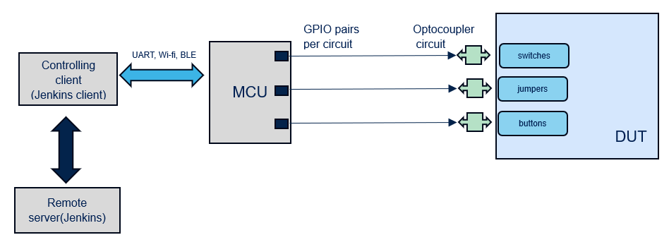 Figure 1: Block diagram of Test Automation Setup
Figure 1 shows the block diagram of automation architecture where a small footprint microcontroller can be used to control an isolation circuit connected to the junctions of switch/jumper/buttons of embedded device under test (DUT). Isolation circuit (e.g., Optocoupler) ensures circuit safety. In the current demonstration NUCLEO-F401RE board (MCU) is used to control the optocoupler circuit connected to boot modes switches and reset button of STM32MP157F-DK2 board under test (DUT). Jenkins will issue remote commands to MCU.
 Figure 2 : Circuit Diagram for controlling HW configurations
Figure 2 demonstrates the circuit diagram where MCU can control the state of two-way Switch SW1. VDD is connected to one end of output and R1 register is added to limit current. The value of R1 is based on the embedded device specification. In the default state, the physical switch is put in off state. Then depending on which boot combination we want, MCU will enable the output side of Optocoupler circuit.
For example, to put STM32MP157F-DK2 in SD card mode, GPIO pair 1 and GPIO pair 2 will be put in HIGH state. This will short output circuit and achieve 1,0,1 combination for SD card boot configuration. A similar circuit is present at the embedded device Reset button. After changing configuration, one can trigger reset to boot in desired hardware configuration.
Jenkins is used to remotely send commands to NUCLEO-F401RE board through a computer containing automation scripts (python and shell scripts) which translates commands to configurations and sends it to MCU to change the device under test (DUT) state as explained above. Using this setup, one can manage all HW configurations remotely. The above arrangement successfully enables the developer to remotely perform board programming / flashing, toggling boot switches and configurations on STM32MP157F-DK2.
 Figure 3: Jenkins pipeline example
Python scripts are present on PC (Jenkins client) controlling MCU and Jenkins is used to invoke these scripts via Jenkins pipeline/scripts.
Scope and Advantages
The proposed solution can be extended to various embedded boards due to the small circuit size that can be easily connected to DUT. Also, a single MCU can control multiple circuits depending on the count of the GPIOs available on a given, multiple DUTs can be controlled. Another advantage being the low cost of circuits and MCU’s and solution is flexible due to multiple options being available to control it (UART, Bluetooth, I2C, SPI, Wi-Fi). Although the solution needs one controlling client which is used to control the Automation system remotely, one client can be used to control multiple Automation systems and thus making the solution scalable and reliable in every aspect as hardware configurations are also tested.
Future work:
Embedded systems can include pin connections at desired switches and buttons, then the need for soldering is eliminated and one can simply connect MCU and isolation circuit to achieve complete and reliable automation.
The post Enhancing Embedded Systems with Automation using CI/CD and Circuit Isolation Techniques appeared first on ELE Times.
Cabinet approves Rare Earth Permanent Magnet Manufacturing Scheme, worth Rs. 7,280 crores
The Cabinet approved the Rs. 7,280 crore Rare Earth Permanent Manufacturing Scheme on November 26, Wednesday. This first-of-its kind initiative aims to establish a six thousand metric tonnes per annum of integrated Rare Earth Permanent Magnet manufacturing in the country.
Cabinet Minister Ashwini Vaishnav, highlighted the importance of Earth Permanent Magnets for electric vehicles, renewable energy, electronics, aerospace, and defence applications at a media briefing in New Delhi. The scheme is expected to support the creation of integrated manufacturing facilities, involving conversion of rare earth oxides to metals, metals to alloys, and alloys to finished Rare Earth Permanent Magnet, the Union Minister added.
As the demand for electric vehicles grows, the demand for permanent magnets is expected to double by 2030. Currently India primarily relies on imports to satisfy its requirements for permanent magnets. This new scheme is expected to play a significant role in generating employment, boosting self-reliance, and accelerating the country’s aim to achieve Net Zero by 2070.
The total duration of the scheme will be seven years from the date of award, including a two-year gestation period for setting up an integrated Rare Earth Permanent Magnet manufacturing facility. The scheme envisions allocating the total capacity to five beneficiaries through a global competitive bidding process.
The post Cabinet approves Rare Earth Permanent Magnet Manufacturing Scheme, worth Rs. 7,280 crores appeared first on ELE Times.
Decoding the Future of Electronics with TI India
In an exclusive conversation with Kumar Harshit, Technology Correspondent, ELE Times, Mr. Kumar details how TI is leading the charge in creating a safer, greener, and smarter world through technology contributions from right here in India and shares his perspective on the future skill sets required for electronics engineers to thrive in the age of artificial intelligence.
Santhosh Kumar, President & Managing Director of Texas Instruments India, discusses the core themes of safety, sustainability, and innovation and outlines the transformative role of AI in shaping the next generation of engineering talent.
Here are the excerpts from the conversation:
ELE TIMES: Given the increasing focus on road safety, particularly for two-wheelers, how is TI leveraging technology to create safer and smarter vehicles?
Santhosh Kumar: Two-wheeler safety is critical, as the rider is the most exposed. We focus on leveraging simple, easy-to-deploy sensing technologies to solve real-world problems. For example, ensuring the side stand is retracted before the vehicle moves is a simple technique, often solved with magnetic sensing connected directly to the engine control. Moving to more advanced safety, we utilize radar and multiple sensors to provide warnings for both sides of the road. We also integrate technology that can help slow or stop a vehicle automatically if the car in front suddenly brakes, even if the rider isn’t fully alert. The goal is to either give the vehicle control to avoid a fatal accident or empower the rider with timely warnings.
ELE Times: TI emphasizes collaboration and community-driven innovation. How important are industry events like Electronica in deepening your relationship with the engineering ecosystem?
Santhosh Kumar: These events are vital for two key interactions. First, our engineers love to work directly with the engineers of our customers. This technical bond is the strongest foundation for creating relevant products. Events like this provide an apt platform for us to build and deepen those relationships. Second, we connect with decision-makers and purchase teams to demonstrate the affordability and worthiness of a product as a feature for mass-market products. Ultimately, innovation doesn’t happen in isolation; it comes from interaction within a community and ecosystem, making these floors essential.
ELE Times: The world is demanding greener technology. Could you outline TI’s commitment to sustainability, both in terms of internal operations and product design?
Santhosh Kumar: We are sensitive to the work we do both inside and outside our factories. Internally, we have a goal to be 100% powered by green energy by 2030, and we are well past 30% today. Furthermore, over 90% of our operational waste is diverted from landfills.
From a product design perspective, we are very sensitive to ensuring our products take up the smallest area and consume the least amount of power. We are always optimizing to create the smallest possible MCU with minimal energy consumption. This approach allows our customers to create products that are inherently greener than they would otherwise have been.
ELE Times: Can you introduce us to TI’s innovative product line in the Power management area?
Santhosh Kumar: We are heavily focused on smart, intelligent systems. A prime example is our Battery Management Systems (BMS), designed and developed in collaboration with engineers in India, ensuring power is used exactly as intended. We have several compelling demos on motor control. India has billions of motors running today, and we are showing how to make them run most efficiently, with the lowest possible cost, without sound, and without losses. You can witness these technologies integrated, such as in our two-wheeler demonstration, combining BMS, motor control, and security features. Given the huge push towards industrial and factory automation in India, we are also showcasing numerous technologies adapted for smarter, more secure, and greener appliances for the 1.4 billion people consuming electricity.
ELE Times: Beyond the automotive and industrial sectors, what are the emerging market segments in India that you see offering significant opportunities for TI’s growth?
Santhosh Kumar: We operate across five core segments, and we see growth in all of them. After automotive and broad industrial (which includes medical electronics, where a lot of Indian innovation is happening), the third key segment is personal electronics. This includes audio, video, and speech, where AI is bringing about a tremendous influx of smarter systems. The large bandwidth and data flow driving these first three segments necessitate our involvement in the communication segment, which forms the backbone. Finally, the enterprise business is the fifth segment. We are seeing customers, product creators, and applications happening in all five areas across India.
ELE Times: Texas Instruments India has been a pioneer for over 40 years. Could you detail the strategic role TIPL plays in driving cutting-edge innovation for TI’s global business units?
Santhosh Kumar: TI India is an important entity to our worldwide business. We have architects, product definers, system engineers, analog and RF designers, and application engineers who manage businesses and contribute to the entire value chain. In fact, many TI’s new products today have a significant contribution from India, including end-to-end product development. We have world-class infrastructure, including labs, benches, and all the necessary equipment in Bangalore, to enable us to contribute to the success of these global products.
ELE Times: Can you share a recent technological breakthrough from TI and define what innovation means to Texas Instruments in the context of solving real-world problems?
Santhosh Kumar: A recent breakthrough we are very excited about is our Gallium Nitride (GaN) solutions. For instance, deploying GaN in two-wheeler chargers can shrink their size by one-third compared to existing technology and significantly reduce power consumption and heat generation due to lower leakage.
To us, innovation extends beyond laboratory research; it is about how we look at real-world problems and use technology to solve them, ultimately enhancing people’s quality of life. We have both an opportunity and a responsibility to improve the lives of eight billion people while preserving the planet.
ELE Times: Talent acquisition is key to sustained innovation. What initiatives does TI India have in place to attract and nurture the next generation of core engineering talent?
Santhosh Kumar: Our strategy is to hire the bright talent directly from campuses, which accounts for 80% of our hiring. To feed this pipeline, we have programs like our Women in Semiconductor and Hardware (WiSH) program, which engages female students beginning in their second year of college. This program provides hands-on experience in core engineering disciplines, including design, testing, verification, and validation. We want to allow a large segment of the population to understand what it means to do core engineering and be a part of world-class product development right here in India.
ELE Times: As a leader who has seen India’s electronics landscape evolve over decades, what is your key message for the industry today?
Santhosh Kumar: The key message is to adopt the technologies happening globally and bring in innovation through new products. This is a tremendous opportunity for India to lead the wave of innovation, to solve real-world problems. We can bring innovation in manufacturing, product development, and applications that lift the quality of life for our people here and for the eight billion people worldwide. With the current energy in the ecosystem and the influx of new players, India can play an important role in driving innovation.
The post Decoding the Future of Electronics with TI India appeared first on ELE Times.
Pages

