
ELE Times

Defence Electronics Warfare Technologies: Designing the Next Generation of Smart Defence Systems
Courtesy DefTech Bharat & DefTech Con Knowledge Desk
Future wars will be won not only by superior weapons, but by superior sensing, networking, electronic dominance, and AI-driven decision-making across the electromagnetic spectrum.
The future battlefield will be defined not merely by firepower but by dominance of the electromagnetic spectrum. Across the world, military planners are investing heavily in electronic warfare (EW), artificial intelligence, software-defined systems, autonomous platforms, and resilient communications. For defence electronics engineers, this transformation presents an unprecedented opportunity to develop agile, intelligent, and rapidly deployable systems capable of operating in highly contested environments.
Recent military operations have demonstrated that information superiority and electronic dominance can determine mission success before the first kinetic strike is launched. The growing convergence of electronic warfare, advanced semiconductors, cognitive computing, and network-centric operations is reshaping how next-generation defence systems are designed.
The Electronic Battlefield Has Changed
Traditional electronic warfare systems were largely platform-centric, consisting of dedicated radar warning receivers, jammers, communication intercept systems, and electronic countermeasures operating independently. Today’s battlefield is radically different.
Modern EW is increasingly becoming a “system-of-systems” architecture where satellites, drones, radars, communication networks, command centers, and autonomous platforms work together as a unified electronic ecosystem.
This shift allows military forces to sense, decide, and act faster than their adversaries. The ability to identify a threat, process intelligence, distribute information, and launch a response within seconds has become a decisive advantage.
For design engineers, the challenge is no longer building standalone equipment but creating modular, networked systems capable of functioning as part of a larger digital battlespace.
Operation Sindoor: A Lesson in Modern Electronic Warfare
India’s Operation Sindoor demonstrated the growing importance of electronic warfare, intelligence fusion, and precision targeting in modern military operations.
While many operational details remain classified, publicly available assessments indicate that the operation reflected a high degree of integration between surveillance systems, communication networks, precision-guided weapons, and command-and-control architectures.
The success of such operations depends heavily on several electronic warfare capabilities:
- Real-time intelligence gathering
- Electronic support measures (ESM)
- Radar and communication signal monitoring
- Secure data networks
- Precision navigation and targeting
- Integrated command systems
The operation highlighted a critical reality of modern warfare: victory increasingly depends on controlling information and the electromagnetic spectrum.
Modern military forces are now investing heavily in systems that can detect enemy emissions, disrupt hostile communications, protect friendly networks, and maintain operational effectiveness even under electronic attack.
Gallium Nitride: The Foundation of Next-Generation RF Systems
One of the most significant advances in defence electronics is the adoption of Gallium Nitride (GaN) semiconductor technology.
Traditional radar and electronic warfare transmitters relied on traveling-wave tubes and other vacuum-tube technologies that required large cooling systems and bulky infrastructure.
For defence designers, this translates directly into reduced Size, Weight, Power, and Cost (SWaP-C).
Modern Active Electronically Scanned Array (AESA) radars, airborne jammers, counter-drone systems, and electronic attack platforms increasingly rely on GaN technology to achieve higher performance within smaller form factors.
The result is the ability to deploy powerful electronic warfare capabilities on tactical vehicles, unmanned systems, and even portable soldier-carried platforms.
Cognitive AI: The New EW Operator
Conventional electronic warfare systems depend on predefined threat libraries. However, modern adversaries employ agile waveforms, frequency hopping, low-probability-of-intercept communications, and adaptive radar systems.
To counter these threats, defence engineers are embedding artificial intelligence directly into EW platforms.
Once a signal is identified, the system can automatically generate optimal jamming, spoofing, or deception strategies without requiring human intervention.
The future electronic battlefield will increasingly be fought by autonomous systems capable of learning and adapting in real time.
Modular Open Systems Architecture (MOSA)
Another major trend transforming defence electronics is the adoption of Modular Open Systems Architecture (MOSA).
Historically, defence systems were highly customized and difficult to upgrade. Introducing a new capability often required extensive hardware redesign.
MOSA changes this paradigm by promoting standardized interfaces and plug-and-play architectures.
At the heart of this approach is the Software-Defined Radio (SDR).
This flexibility dramatically reduces lifecycle costs and accelerates technology refresh cycles.
As threats evolve faster than traditional procurement cycles, MOSA provides a practical path to continuous capability enhancement.
GNSS-Free Navigation: Operating When GPS Fails
One of the most important lessons from contemporary conflicts is the vulnerability of satellite navigation systems.
GPS jamming and spoofing have become routine tactics on modern battlefields.
As a result, defence designers are increasingly focusing on GNSS-independent navigation solutions.
Emerging systems combine:
- Inertial Navigation Systems (INS)
- Terrain contour matching
- Visual navigation
- RF beacon triangulation
- LTE and 5G positioning
- Sensor fusion algorithms
Artificial intelligence combines these inputs to maintain accurate positioning even when satellite signals are unavailable.
For autonomous systems, missiles, drones, and tactical vehicles, GNSS resilience is rapidly becoming a mission-critical capability.
AI-Driven SWaP-C Optimization
The pressure to reduce Size, Weight, Power, and Cost continues to influence every defence program.
Machine learning is now being used to optimize engineering trade-offs before physical prototypes are built.
AI-assisted design platforms can evaluate:
- RF chain performance
- Thermal management
- Antenna placement
- Power consumption
- Electromagnetic compatibility
- Structural constraints
Digital twin technology allows engineers to test thousands of virtual configurations, dramatically reducing development time and improving design quality.
The integration of AI into the design process is becoming as important as AI within the deployed system itself.
DefTech Bharat: Accelerating India’s Defence Innovation Ecosystem
As India’s defence technology ecosystem expands, industry platforms are playing a critical role in connecting innovators, manufacturers, startups, system integrators, armed forces, and policymakers.
DefTech Bharat is an innovation-led defence technology platform that brings together companies, engineers, startups, OEMs, and government stakeholders to showcase next-generation solutions across defence electronics, software, hardware, testing, telematics, AI, drones, quantum technologies, autonomous systems, and cyber defence. For innovators working on electronic warfare, secure communications, GaN-based RF hardware, modular SDR platforms, and GNSS-resilient navigation, it provides a timely venue to demonstrate technologies, exchange ideas, and build partnerships with the wider defence ecosystem. By combining exhibition, technical engagement, and B2B networking, DefTech Bharat positions itself as a launchpad for rapidly deployable, out-of-the-box defence solutions.
For innovators developing:
- Electronic warfare systems
- AI-enabled defence platforms
- Software-defined radios
- GaN-based RF solutions
- Counter-drone technologies
- Autonomous vehicles
- Secure communication systems
DefTech Bharat provides a valuable opportunity to demonstrate capabilities, interact with defence stakeholders, and explore collaborative development opportunities.
The platform enables technology providers to showcase working prototypes, advanced subsystems, and deployable solutions to government agencies, defence organizations, OEMs, and strategic partners.
As India pursues self-reliance in defence technologies under the Atmanirbhar Bharat initiative, such platforms serve as catalysts for innovation, commercialization, and technology transfer.
The post Defence Electronics Warfare Technologies: Designing the Next Generation of Smart Defence Systems appeared first on ELE Times.
Brain-Computer Interfaces (BCIs) & Neurotechnology: The Next Frontier in Electronics Engineering
The convergence of neuroscience, electronics, and artificial intelligence is driving one of the most transformative technological revolutions of the 21st century: Brain-Computer Interfaces (BCIs) and neurotechnology. Once confined to science fiction, BCIs are now rapidly evolving into practical systems capable of enabling direct communication between the human brain and external electronic devices. For electronics engineers, this emerging domain offers exciting opportunities in embedded systems, signal processing, flexible electronics, biomedical instrumentation, and AI-driven hardware development.
The Rise of Brain-Computer Interfaces
A Brain-Computer Interface is a system that acquires neural signals, processes them, and translates them into commands for computers, prosthetics, or other electronic systems. Traditional BCIs relied on electroencephalography (EEG), where electrodes placed on the scalp measure brainwave activity. While non-invasive EEG systems remain important for research and healthcare applications, recent advances in high-density electrode arrays and implantable bioelectronics are dramatically improving signal quality and functionality.
Modern BCIs can now interpret neural activity with remarkable precision, enabling paralyzed individuals to control robotic limbs, type text using thought alone, and even regain limited speech capabilities. The integration of machine learning algorithms with neural signal acquisition hardware has accelerated these developments significantly.
Flexible Bioelectronics: A Game Changer
One of the biggest engineering challenges in neurotechnology has been the mechanical mismatch between rigid electronic devices and soft biological tissues. Conventional silicon-based implants often trigger inflammation or degrade over time due to tissue damage. Flexible bioelectronics are solving this issue.
Flexible neural interfaces are built using biocompatible materials such as polyimide, graphene, conductive polymers, and ultra-thin gold traces. These devices can bend and stretch with brain tissue, reducing long-term damage and improving signal stability. Engineers are also exploring bioresorbable electronics that safely dissolve in the body after completing their function.
For electronics engineers, flexible electronics require innovation in several areas:
- Low-power integrated circuit design
- Stretchable conductive materials
- Miniaturized sensor architectures
- Wireless power transfer systems
- High-speed neural signal amplification
These systems must operate reliably while consuming extremely low power to minimize heat generation near sensitive neural tissue.
High-Density Electrode Arrays and Neural Mapping
High-density electrode arrays are enabling researchers to record thousands of neurons simultaneously. Companies and research institutions are developing microelectrode arrays with unprecedented spatial resolution, allowing detailed mapping of neural activity patterns.
Advanced semiconductor fabrication techniques are making it possible to integrate thousands of microscopic electrodes onto a single chip. These arrays are combined with custom ASICs (Application-Specific Integrated Circuits) for signal amplification, filtering, analog-to-digital conversion, and wireless communication.
The data bandwidth generated by these systems is enormous. A next-generation BCI may process gigabits of neural data every second, creating major opportunities for engineers specializing in:
- Edge AI processing
- FPGA-based neural computing
- Real-time DSP systems
- Wireless telemetry
- Neuromorphic processors
Neuromorphic engineering, inspired by the architecture of the human brain, is becoming particularly important for efficient neural data processing. Unlike conventional processors, neuromorphic chips mimic biological neural networks and consume significantly less power.
Applications Transforming Healthcare
Healthcare remains the most promising application area for BCIs and neurotechnology. Neuroprosthetics are helping amputees control robotic limbs using brain signals with increasing accuracy and natural movement. Cochlear implants and retinal prostheses are restoring sensory functions to patients with hearing and vision impairments.
In neurological diagnostics, implantable neural sensors can monitor epilepsy, Parkinson’s disease, and other disorders in real time. Closed-loop neurostimulation systems can detect abnormal brain activity and automatically deliver corrective electrical stimulation.
Researchers are also investigating memory enhancement, depression treatment, and cognitive rehabilitation through targeted neural stimulation. These advancements depend heavily on reliable biomedical electronics and ultra-low-noise analog front-end design.

Patient controlling robotic prosthetic arm using BCI technology
Challenges and Ethical Considerations
Despite rapid progress, significant challenges remain. Neural signals are extremely weak and susceptible to noise, requiring sophisticated filtering and signal conditioning techniques. Long-term implant reliability, cybersecurity, and wireless communication safety are also major concerns.
Ethical issues surrounding cognitive enhancement, neural privacy, and brain data ownership are becoming increasingly important. As BCIs evolve from medical devices to consumer technologies, electronics engineers will play a critical role in designing secure and responsible systems.
Power management is another key challenge. Implantable devices require efficient energy harvesting or wireless charging technologies to avoid repeated surgical battery replacement. Advances in ultra-low-power electronics and energy-efficient communication protocols will be essential.
The Future of Neurotechnology
The future of BCIs lies in seamless human-machine integration. Emerging systems may eventually enable direct brain-to-brain communication, immersive virtual reality control, and advanced cognitive augmentation. Artificial intelligence combined with adaptive neural interfaces could create highly personalized neuroprosthetic systems capable of learning and evolving with users.
For electronics engineers, neurotechnology represents a multidisciplinary field where expertise in electronics, embedded systems, materials science, AI, and biomedical engineering converge. As the boundaries between biology and electronics continue to blur, BCIs are poised to become one of the defining technologies of the coming decades.
The era of intelligent bioelectronic systems has begun — and electronics engineers are at the center of this technological transformation.
The post Brain-Computer Interfaces (BCIs) & Neurotechnology: The Next Frontier in Electronics Engineering appeared first on ELE Times.
Brain-Inspired Neuromorphic Computing: Moving Beyond Traditional Processor Architectures
For more than five decades, the computing industry has relied on the von Neumann architecture, where memory and processing units are physically separated. While this architecture has enabled remarkable advances in computing power, it also faces significant challenges in today’s data-driven world. The continuous movement of data between memory and processors consumes enormous amounts of energy and creates performance bottlenecks, particularly in artificial intelligence (AI) and edge computing applications.
To address these limitations, researchers and semiconductor companies are increasingly turning to a radically different approach inspired by nature’s most efficient computing system—the human brain. Neuromorphic computing represents a paradigm shift in processor design, enabling machines to process information more like biological neural networks while consuming a fraction of the energy required by conventional systems.
Understanding Neuromorphic Computing
Neuromorphic computing refers to the design of hardware systems that mimic the structure and operation of the human brain. Unlike traditional processors that execute instructions sequentially, neuromorphic chips consist of artificial neurons and synapses that operate in parallel and communicate through event-driven signals known as spikes.
The human brain contains approximately 86 billion neurons interconnected through trillions of synapses. Despite this immense complexity, the brain operates on roughly 20 watts of power—less than many household light bulbs. Neuromorphic engineers aim to replicate this extraordinary efficiency in silicon.
In a neuromorphic system:
- Artificial neurons process incoming signals.
- Synapses store connection strengths and learning parameters.
- Information is transmitted only when meaningful events occur.
- Memory and computation are closely integrated.
- Learning can occur directly on the device.
This architecture significantly reduces the energy and latency associated with moving data between separate memory and processing units.
Why Traditional Architectures Are Reaching Their Limits
Modern AI applications generate enormous volumes of data from sensors, cameras, microphones, and connected devices. Conventional CPUs and GPUs must continuously shuttle this data between memory and processing cores, creating what is commonly known as the “memory wall.”
Key limitations include: High Power Consumption, Latency Challenges and Scalability Constraints. Neuromorphic computing addresses these challenges by bringing memory, learning, and processing closer together in a brain-like architecture.
Event-Driven Processing: The Key to Efficiency
One of the most innovative aspects of neuromorphic systems is event-driven computation. Traditional processors operate continuously, executing clock cycles whether useful work is being performed or not. Neuromorphic chips, however, remain largely inactive until significant events occur.
For example, consider a surveillance camera monitoring a quiet corridor. A conventional AI processor continuously analyzes every video frame. A neuromorphic processor only activates when movement or a meaningful change is detected. The result is intelligent systems that can remain operational for extended periods without frequent charging or cloud connectivity.
Real-Time Learning at the Edge
One of the most promising capabilities of neuromorphic hardware is on-device learning. Traditional AI systems are typically trained in data centers and deployed as fixed models. Updating these models often requires cloud access, large datasets, and significant computational resources.
Neuromorphic chips can adapt continuously based on experience, much like biological brains. This capability enables: Personalized Wearables, Autonomous Robots, Smart Sensors and Adaptive Industrial Systems. Such capabilities are particularly valuable in environments where network connectivity is limited or unavailable.
Applications Across Industries: Autonomous Vehicles: Self-driving vehicles process enormous amounts of sensory information from cameras, radar, LiDAR, and ultrasonic sensors. Healthcare and Wearables: Smart medical devices require continuous monitoring while maintaining long battery life. Industrial Automation: Factories increasingly rely on intelligent edge devices for predictive maintenance, quality inspection, and process optimization. Aerospace and Defense: Autonomous drones and surveillance systems benefit from low-power AI processing capable of operating independently in challenging environments. Internet of Things (IoT): Billions of connected devices generate vast quantities of sensor data.
Leading Neuromorphic Hardware Developments
Several organizations are actively advancing neuromorphic technology: Intel Corporation has developed the Loihi family of neuromorphic research chips capable of on-chip learning and adaptive processing. IBM pioneered large-scale neuromorphic architectures with its TrueNorth processor. European Human Brain Project has invested heavily in brain-inspired computing research. Numerous startups are developing specialized neuromorphic solutions for edge AI, robotics, and industrial applications.
Technical Challenges Ahead
Despite significant progress, neuromorphic computing remains an emerging field. Key challenges include: Programming Complexity: Developing software for spiking neural networks differs substantially from conventional programming methodologies. Ecosystem Maturity: Tools, frameworks, and standards remain less mature than those available for CPUs, GPUs, and traditional AI accelerators. Commercial Scalability: Manufacturing and integrating neuromorphic hardware into mainstream products requires further technological advancement and industry adoption. Benchmarking Difficulties: Comparing neuromorphic performance against conventional systems remains challenging because the architectures operate fundamentally differently.
The Future of Brain-Inspired Computing
As AI increasingly moves from centralized data centers to intelligent edge devices, energy efficiency and real-time adaptability become critical requirements. Neuromorphic computing offers a compelling solution by emulating the principles that make the human brain remarkably powerful and efficient.
Rather than replacing traditional CPUs and GPUs entirely, neuromorphic processors are likely to emerge as specialized accelerators for applications requiring low power consumption, continuous learning, and rapid decision-making at the edge.
For working engineers, neuromorphic computing represents more than just another processor innovation. It signals the beginning of a new computing paradigm where machines learn, adapt, and respond with unprecedented efficiency. As edge AI, robotics, autonomous systems, and wearable technologies continue to expand, brain-inspired architectures may become a foundational component of next-generation intelligent systems.
Neuromorphic computing is redefining how engineers think about processing, memory, and intelligence. By mimicking the brain’s structure and operation, neuromorphic chips achieve remarkable energy efficiency while enabling real-time learning and adaptation.
The post Brain-Inspired Neuromorphic Computing: Moving Beyond Traditional Processor Architectures appeared first on ELE Times.
AI-Augmented Test Automation: Transforming Enterprise-Scale System Validation
Enterprise software is no longer built for stability. It is built for continuous change. Modern systems evolve over distributed architectures, cloud-native platforms, and microservice ecosystems, with release cycles measured in days rather than months. Against this rapid evolution, the customary boundaries of testing are being fundamentally redefined.
Validation, once a discrete phase in the development lifecycle, now operates under constant pressure to keep pace with rapid deployment. The challenge is no longer simply guaranteeing correctness, but doing so continuously, at scale, and amid mounting system complexity.
Conventional automation frameworks, designed for predictability and control, are beginning to show their limitations. As systems evolve dynamically, static test scripts and rule-based execution models struggle to remain effective. It is within this context that AI-augmented test automation is emerging not as a replacement, but as an essential evolution of how enterprise systems are validated.
From Scripted Automation to Adaptive Testing SystemsTraditional automation has long relied on predefined scripts and deterministic workflows. While this strategy delivers consistency, it is inherently rigid. Even minor changes in application interfaces or workflows is able to disrupt test execution, causing frequent maintenance cycles that consume time and engineering effort.
AI introduces adaptability into this equation, fundamentally shifting the testing landscape. By using historical data, execution patterns, and system behaviour, AI-augmented frameworks can interpret changes and operate dynamically. As a result, testing systems begin to move past static execution toward context-aware validation, where decisions are informed by data rather than predefined rules alone.
This shift isn’t incremental; it is a redefinition of automation itself. Testing no longer centres solely on executing what is known, but on intelligently responding to what changes. As Satya Nadella has emphasised, “Every company is becoming a software company, and agility is key regarding innovation.” In such an environment, testing must evolve into an enabler of that agility, not a constraint on it.
The Scaling Challenge: Complexity at Enterprise LevelAt enterprise scale, testing is not simply about validating features—it is about ensuring the coordinated functioning of distributed systems. Applications span multiple services, environments, and configurations, each introducing its own layer of variability.
What makes this challenge particularly significant is not just the volume of test cases, but the rate at which they become outdated. As systems change, test suites expand, execution times increase, and maintenance overhead grows disproportionately.
The core pressures can be summarized as:
- Expanding and continuously evolving test suites
- Increasing difficulty in maintaining reliable test execution
- The need for comprehensive coverage across diverse system states
These challenges do not scale linearly—they compound. Without intelligent optimization, testing becomes a bottleneck, slowing down the very innovation it is meant to support. AI-augmented automation addresses this by introducing prioritization, reducing redundancy, and aligning testing efforts with actual system risk.
Resilience Through Self-Healing AutomationOne of the most tangible advancements enabled by AI is the concept of self-healing automation. In traditional systems, test failures often result from minor interface changes—renamed elements, altered layouts, or modified identifiers. These failures require manual intervention, creating inefficiencies in otherwise automated workflows.
AI-driven systems mitigate this limitation by recognizing patterns and relationships within application structures. Instead of failing immediately, they can identify alternative elements or pathways, allowing tests to continue execution. This capability significantly reduces maintenance cycles and enhances overall system resilience.
More importantly, it shifts the role of automation from a fragile executor to a robust validation layer capable of adapting alongside the applications it tests.
Intelligent Test Design: From Coverage to Risk-Based ValidationA critical evolution in AI-augmented testing also lies in how test cases are generated and optimised. Established approaches often prioritise exhaustive coverage, leading to large but inefficient test suites. In contrast, AI enables a more strategic model—one that focuses on risk, impact, and system operation.
More specifically, by analysing historical defects, usage patterns, and code changes, AI systems can identify which areas of an application are most likely to fail and prioritise testing accordingly. This switch from coverage-driven to risk-based validation amounts to a significant improvement in both capability and effectiveness.
Instead of attempting to execute all possible scenarios, testing becomes targeted and adaptive, ensuring that critical paths receive the highest level of scrutiny, thus increasing the effectiveness of the entire process.
Continuous Testing in High-Velocity PipelinesIntegrating testing into CI/CD pipelines has fundamentally changed how software is delivered. While the speed of these pipelines is transformative, it also introduces challenges. Testing must provide rapid, reliable feedback without becoming a performance bottleneck.
AI addresses this by introducing decision intelligence into test execution. Rather than running all tests indiscriminately, systems select and prioritise tests based on relevance to recent changes. This reduces execution time while maintaining validation quality.
In this model, testing is no longer a passive checkpoint; it becomes an active, intelligent participant in the delivery pipeline, continuously adjusting to the system’s evolving state.
From Test Execution to Quality Intelligence
Looking beyond automation and execution, AI delivers a wider transformation: the evolution of testing into a source of engineering intelligence. By analysing large volumes of test data, system logs, and defect histories, AI systems can discover patterns that inform not only testing strategies but also system design decisions.
This shift repositions testing from a reactive activity to an anticipatory capability. Instead of identifying defects after they occur, systems can predict possible failure points and guide engineering efforts toward more robust designs.
In this sense, testing acts not only as a validation function but also as a contributor to overall system quality and reliability.
Human Expertise in an AI-Augmented EcosystemDespite the growing role of AI, human expertise remains central to the testing process. AI excels at handling scale, pattern recognition, and repetitive execution, but it lacks contextual judgment and domain-specific insight.
Human testers bring critical thinking, scenario understanding, and strategic supervision capabilities that cannot be fully automated. The most effective testing environments are therefore not AI-driven in isolation, but AI-augmented, where people and computers’ capabilities complement each other.
This balance ensures that, as efficiency improves, the depth and reliability of validation are not compromised.
Adoption Realities: Engineering and Integration ChallengesThe adoption of AI-augmented testing is not free from challenges. Integrating intelligent systems into existing enterprise environments requires careful planning, particularly in data quality, tool compatibility, and workflow alignment.
Organisations must ensure sufficient data is available to train AI models effectively, while also preserving transparency in decision-making. Integration with legacy systems can make deployments more complex, requiring incremental adoption strategies.
These considerations highlight an important reality: the transition to AI-augmented testing is as much an organisational shift as it is a technological one.
Future Outlook: Toward Autonomous Testing EcosystemsGoing forward, the trajectory of test automation points toward increasing autonomy. AI systems are expected to take on more responsibility in managing test lifecycles, from generation and execution to optimisation and maintenance.
Future systems will not only execute tests but also constantly learn from outcomes, improving strategies and adjusting to evolving system behaviour. This progression moves testing closer to a self-sustaining ecosystem, where validation progresses alongside the software it supports.
As Sundar Pichai has noted, “AI is one of the most profound technologies we are working on.” Its application in testing demonstrates a broader transformation, one in which intelligence becomes embedded in the core of engineering processes.
Conclusion: Redefining the Role of Testing in Enterprise SystemsAI-augmented test automation represents more than an enhancement of existing practices; it constitutes a fundamental change in how enterprise systems are validated. In an age distinguished by speed, scale, and complexity, established approaches are no longer sufficient.
Testing must evolve into an intelligent, adaptive capability, one that not only verifies system operation but also actively contributes to its reliability and dependability. AI enables this transformation by introducing adaptability, insight, and capability into every stage of the testing lifecycle.
As enterprise systems continue to grow in complexity, the role of AI in testing will become increasingly central. The future of quality assurance will not be defined by how extensively systems are tested, but by how intelligently they are validated consistently, efficiently, and at scale.
The post AI-Augmented Test Automation: Transforming Enterprise-Scale System Validation appeared first on ELE Times.
Advances in core technologies for semiconductor manufacturing
By Tzu-Yi Lee
Revolutionizing semiconductor fabrication, ALD, ALE, and NBE deliver atomic-scale precision, driving unprecedented performance and scalability in next-generation miniaturized devices.
With the rapid growth of the semiconductor industry, Moore’s law has become a core guiding principle for the continuous advancement of electronic devices. Moore’s law predicts that the number of transistors will double every two years, a trend that is driving the continued reduction in device and circuit size. As the size of semiconductor devices shrinks further, the complexity and accuracy of the manufacturing process increase dramatically, requiring the introduction of ultra-precision and ultra-fine technologies into the semiconductor process to ensure device performance and reliability. Among these technologies, etching and deposition are particularly crucial as they form the foundation for achieving high-performance semiconductor devices. They play an essential role in enabling device miniaturization and increasing functional density. Fig. illustrates the trend in semiconductor manufacturing technology from 2000 to 2035, reflecting advancements beyond Moore’s law and incorporating more-than-Moore principles. As transistor technology evolves to Integrated Circuit (IC) evolves, we can see a progression from scale devices and wires to scale basic logic units to scale system functions. Early developments in transistor technology, such as geometric scaling at the 90 nm node, included introducing strained Si and using copper (Cu) for back-end-of-line (BEOL) interconnections. Over time, technological advances drove transistors to 40 nm and 28 nm nodes, when the use of high-k gate dielectrics and metal gate technologies appeared, marking the era of equivalent scaling. With the further development of process technology, from 20 nm to 7 nm, transistor technology entered the era of heterogeneous scaling (post-Moore scaling), which included the widespread use of fin field-effect transistors (FinFETs). FinFETs provide superior channel control due to their three-dimensional structure, which allows the gate to surround the channel on multiple sides, enhancing gate control and reducing short-channel effects. In recent years, the introduction of gate-all-around (GAA) transistors, an advanced technology, has further shrunk device size and provided better control of short-channel effects, reduced leakage current, and enhanced switching performance. As technology nodes advance to 5 nm and beyond, innovations such as GAA transistors provide better control of short-channel effects, reduced leakage, and enhanced performance. Future scaling is expected to incorporate compound field-effect transistors (CFETs), 2D semiconductors, and hybrid integration, which not only sustain Moore’s law but also expand into more-than-Moore functionalities, such as photonic integration, quantum technologies, and neuromorphic computing. These advancements heavily rely on nanoscale etching and deposition processes, such as atomic layer deposition (ALD), atomic layer etching (ALE), and neutral beam etching (NBE), which are critical in achieving the precision and performance required for next-generation devices. This article shows how these advanced techniques drive semiconductor fabrication, supporting continued progress and enabling breakthroughs beyond Moore’s law.
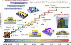
Fig. 1. Evolution of transistor density and gate length in ICs.
Definition and backgroundThe etching process involves removing a material from a surface through chemical or physical methods, which typically plays a key role in semiconductor manufacturing. Precise control of this process, including major factors such as etch depth, etch profile, surface roughness, and uniformity, is critical to ensuring the performance and reliability of micro- and nanoelectronic devices. Wet etching, which utilizes a chemical reaction in a bath environment, is known for its low cost, ease of implementation, and high material selectivity. Conversely, dry etching is performed through physical and chemical reactions in a vacuum chamber, providing greater precision depth control, profile selectivity, and the ability to define critical feature dimensions.
Atomic layer etching (ALE)ALE is a highly precise technique critical for fabricating nanoscale semiconductor devices. By alternating between adsorption and reaction steps, ALE achieves the removal of single atomic layers per cycle, providing exceptional control and minimizing surface roughness. This method, derived from ALD techniques, involves sequential exposure to different reactive gases, with intermediate purging steps to ensure precise layer-by-layer removal and maintain atomic-scale accuracy. ALE is particularly advantageous in the fabrication of advanced 3D integrated circuits (3D ICs) and memory devices. In 3D IC manufacturing, ALE addresses the challenges of creating complex 3D transistor architectures, such as GAA and multi-bridge-channel FETs (MBCFETs). By enabling atomic-scale etching, ALE provides exceptional control over morphology and depth, ensuring precise patterning for nanoscale features.
Neutral-beam etching (NBE)NBE represents a significant advancement in the etching processes for GaN-based HEMTs and light-emitting diodes (LEDs). This method effectively addresses the critical challenge of plasma-induced damage, which is prevalent in conventional etching techniques such as ICP-RIE. GaN materials are highly valued in the semiconductor industry for high-power and high-frequency applications. However, achieving normally-off operation in GaN-based HEMTs remains challenging due to the plasma-induced damage associated with techniques such as gate recessing. NBE offers a potential solution to minimize such damage and enhance device performance.
Deposition techniquesThin film technology is an advanced approach aimed at improving the structural, electrical, magnetic, optical, and mechanical properties of bulk materials. It has found widespread application in semiconductor devices, integrated circuits, transistors, liquid crystal displays, light-emitting diodes, solar cells, sensors, and micro-electromechanical systems (MEMSs). The distinctive properties of thin film materials are crucial for the technological advancement of various electronic, electrical, magnetic, and optical devices. These films are created using various physical or chemical methods, each of which is essential for producing ultra-thin materials known for their uniform, conformal, and controllable thickness. As atomic and near-atomic scale manufacturing (ACSM) evolves, the necessity of depositing high-quality, impurity-free thin films for laminated structures becomes crucial.
The future of ALD, ALE, and NBE technologies is promising as ongoing advancements continue to address the evolving demands of semiconductor manufacturing. Numerous optimization strategies have been employed to enhance their precision and efficiency. In particular, controlling deposition thickness in ALD, achieving atomic-level etching with ALE, and minimizing surface damage through NBE have proven crucial for improving device performance. Geometrical parameters such as layer thickness, etch depth, and surface passivation have significant impacts on device reliability and durability. Addressing thermal management, particularly in high-power applications, becomes essential as devices scale further. Future efforts could explore the use of more thermally conductive substrates and the refinement of etching profiles to minimize defects and improve device performance. Additionally, optimizing contact technologies to reduce resistance and ensure smooth surface morphology will be critical. Looking ahead, further research should focus on enhancing the uniformity and precision of these processes for advanced applications in micro-LEDs, high-speed communications, and optoelectronics. Future research should consider the performance capabilities of ALD, ALE, and NBE technologies to promote the development of next-generation semiconductor devices.
The post Advances in core technologies for semiconductor manufacturing appeared first on ELE Times.
UP Cabinet Amends 2024 Semiconductor Policy to Boost Investment
The state cabinet on Wednesday approved an amendment to the state’s Semiconductor Policy-2024 to fine-tune and adapt it to specific needs under the India Semiconductor Mission. Officials said the amendment would provide greater flexibility to investors. An official said that the move would accelerate the establishment of semiconductor units, support India’s efforts to build a domestic semiconductor ecosystem, and reduce dependence on imports of critical eleсtronic components. An official spokesperson said that the changes were aimed at providing policy support for investors and aligning the framework with the Centre’s India Semiconductor Mission. The Semiconductor Policy-2024 was notified on Jan 19, 2024, and will remain in force for five years. Officials said that the amendments would not entail any additional financial burden on the state exchequer.
The post UP Cabinet Amends 2024 Semiconductor Policy to Boost Investment appeared first on ELE Times.
Murata Introduces World’s First 2.2μF/100Vdc Soft-Termination Chip MLCC in 0805-inch Size for Automotive Applications
Murata Manufacturing Co., Ltd. introduces the GCJ21BD72A225KE02, a soft-termination chip multilayer ceramic capacitor (MLCC) for automotive powertrain and safety equipment. This world’s first soft-termination chip MLCC product achieves the highest available capacitance of 2.2μF at 100Vdc in the smallest 0805-inch (2.0×1.25mm) size.
As vehicle electrification accelerates and autonomous driving (AD) and advanced driver-assistance systems (ADAS) grow more sophisticated, engineers face increasing pressure to pack more functionality into tighter board spaces. The wider adoption of 48V power systems further demands components that combine high capacitance, high voltage tolerance, and a small footprint. At the same time, mechanical stress from board flexure, due to vibration and thermal cycling while driving, remains a reliability concern. The GCJ21BD72A225KE02 addresses all these challenges.
Built on Murata’s proprietary ceramic material design, including fine particle size and uniformity control, the soft-termination chip MLCC achieves 2.2μF at 100Vdc in the 0805-inch size, a rating previously only possible in the larger 1206-inch (3.2×1.6mm) size. The result is an approximately 51% reduction in board mounting area compared to Murata’s previous 2.2μF/100Vdc offering, and an approximately 2.2x increase in capacitance over its previous 0805-inch, 100Vdc product. Soft termination further enhances field reliability by absorbing board flexure stress and reducing post-mount cracking.
The GCJ21BD72A225KE02 supports an operating temperature range of -55°C to +125°C and meets X7T temperature characteristics per EIA standards. Murata will continue expanding its automotive-grade MLCC lineup, delivering the miniaturization, high capacitance, high voltage ratings, and reliability that next-generation vehicles demand.
The post Murata Introduces World’s First 2.2μF/100Vdc Soft-Termination Chip MLCC in 0805-inch Size for Automotive Applications appeared first on ELE Times.
Qorvo Eliminates Negative Bias in New RF Control Portfolio
Qorvo, a leading global provider of connectivity and power solutions, announces a new portfolio of silicon-on-insulator (SOI) RF switches and digital step attenuators (DSAs) for defense, aerospace, and infrastructure customers. This new portfolio simplifies RF system design, reduces BOM complexity, and accelerates integration in wideband systems.
These new solutions address growing system demands for broader frequency coverage, agile signal routing, and optimal integration without the complexity of legacy GaAs-based RF control component approaches or multi-vendor RF control chains. With TTL-compatible control that eliminates the need for a negative voltage rail, Qorvo’s SOI portfolio helps designers simplify biasing networks, reduce BOM count, streamline board layouts while maintaining the fast-switching speeds, high isolation, and high linearity required in defense and aerospace applications. The portfolio gives designers a simpler alternative to legacy RF control approaches that require negative bias rails, multiple control components, and more complex board-level integration.
“Customers are looking for ways to simplify RF control architectures without sacrificing the switching speed and RF performance required in modern defense systems,” said Doug Bostrom, general manager of Qorvo’s Defense and Aerospace business. “By eliminating the need for a negative voltage rail, our SOI portfolio helps reduce design complexity, streamline integration, and provide a faster path from design to deployment.”
| Product | Function | Frequency Range | Key Differentiators | Target Applications |
| QPC2320 | Reflective SPDT Switch | Up to 15 GHz | Low insertion loss, high isolation, high linearity, <50 ns switching | Radar, EW, secure communications |
| QPC2420 | Reflective SPDT Switch | Up to 30 GHz | Wideband coverage, high linearity, fast switching, compact footprint | Wideband radar, SATCOM, test & measurement |
| QPC2180 | Reflective SP8T Switch | Up to 8 GHz | High linearity for filter banks, compact integration | Filter banks, multi-band radios |
| QPC5330 | 6-bit Digital Step Attenuator | Up to 15 GHz | Precise attenuation, glitch-safe operation, SPI/I2C control | Signal conditioning, radar/EW |
| QPC5430 | 6-bit Digital Step Attenuator | Up to 30 GHz | Wideband attenuation, high linearity, daisy-chain support | Test & measurement, microwave backhaul, communications systems |
Unlike conventional approaches that rely on multiple narrowband components or mixed-vendor solutions, Qorvo’s SOI portfolio enables designers to standardize switch and attenuator functions into a scalable RF control platform. This reduces routing complexity, minimizes calibration effort, and accelerates design reuse across programs. In comparison to legacy GaAs switches, Qorvo delivers simpler biasing and easier integration while maintaining RF performance for modern defense and aerospace systems. With discrete multi-part RF control chains, designers can reduce BOM complexity, board space, and integration burden while improving signal integrity and simplifying future upgrades.
The portfolio aligns with key industry trends, including wider bandwidth radar and EW systems, more agile signal routing requirements, and increasing pressure to reduce SWaP while accelerating time to market. By combining optimal control integration, fast switching, high isolation, strong linearity, and flexible digital control, Qorvo enables designers to modernize RF control architectures without increasing system complexity.
The post Qorvo Eliminates Negative Bias in New RF Control Portfolio appeared first on ELE Times.
Rohde & Schwarz Secures Critical Certification for Next-Gen eCall Compliance
The hybrid eCall test specification EN 18052 states that a hybrid system must combine different transmission paths and protocols to make sure an eCall reliably reaches its destination. In practice, this means a vehicle uses NG eCall functions (IP/IMS-based voice and data over 4G/5G) but can automatically fall back to available classic CS eCall (2G/3G) transport paths when coverage or service quality degrades. Manufacturers need to validate hybrid implementations to ensure they can trigger calls, transmit the minimum set of data (MSD), maintain GNSS positioning, and deliver intelligible voice quality across multiple network scenarios, including voice over New Radio (VoNR), voice over LTE (VoLTE), and circuit-switched fallback. Tests must demonstrate that a system remains robust during handovers and under degraded radio conditions, while also complying with relevant CEN, ETSI, 3GPP, and national requirements.
“We use the solution for functional tests and protocol conformity tests as well as for the type-approval of In-Vehicle Systems (IVS) that implement hybrid eCall and NG eCall,” says Thomas Reschka, Senior Technical Consultant at cetecom advanced.
Rohde & Schwarz has updated its eCall evaluation solution, CMX-KA09x, to support compliance with EN 18052:2025 and EN 17240:2024+A1:2026. The CMX-KA099 option completed Public Safety Answering Point (PSAP) test scenarios in accordance with EN 18052:2025, while the CMX-KA098 option completed PSAP test scenarios in accordance with EN 17240:2024+A1:2026. This marks an important step toward meeting European requirements for NG eCall test systems. The test environment allows the simulation of the real world mobile network conditions and the emulation of various network scenarios. This is a significant advantage in preparing for certifications or the market launch of new vehicle models.
The post Rohde & Schwarz Secures Critical Certification for Next-Gen eCall Compliance appeared first on ELE Times.
XpressConnect PCIe 6.0: Solving AI Data Center Latency
As AI workloads continue to scale, the data center architects show limitations by signal reach and rising latency, leaving valuable memory resources underutilized across large GPU clusters. These challenges boost as interconnect speeds increase. At 64 GT/s (giga transfers per second), signal integrity limitations can restrict system scale and burden server architectures. In response, Microchip Technology releases XpressConnect PCIe 6.0 and CXL 3.1 retimers to enable memory expansion and resource disaggregation in large-scale AI fabrics.
The retimers extend signal reach beyond conventional PCIe Gen 5 and Gen 6 electrical limits, enabling more flexible system designs across complex baseboards, riser cards, and cabled interconnects. The retimers are engineered to help address these challenges by enabling higher-bandwidth connectivity while supporting the stringent thermal requirements of modern AI fabrics that require power budgets. XpressConnect retimers achieve a pin-to-pin latency of less than 12 ns, approximately 80% lower than PCIe 6.0 specifications. This low-latency performance helps improve utilization of AI accelerators and GPUs by reducing data stalls in high-density AI clusters.
“AI data centers are increasingly constrained not by compute, but by the ability to move data efficiently across the system. As PCIe 6.0 pushes speeds to 64 GT/s, signal reach and latency become critical design challenges,” said Brian McCarson, corporate vice president and GM of Microchip’s data center solutions business unit.
Our XpressConnect retimers are designed to act as the high‑performance nerve center of the AI server, helping customers build more scalable, power‑efficient fabrics by reducing latency and improving connectivity across dense GPU clusters. This system‑level approach allows data center architects to reclaim underutilized resources and improve overall platform efficiency at scale.
The XpressConnect retimers round out Microchip’s data center portfolio and are engineered to work alongside the company’s 3-nm Switchtec PCIe Gen 6 switches, Adaptec SmartRAID controllers and Host Bus Adapters (HBAs), and Flashtec NVMe controllers, helping enable a pre-validated, interoperable fabric. Microchip’s XpressConnect PCIe Gen 6 and CXL 3.1 retimers can integrate with PCIe Gen 3, Gen 4, and Gen 5 platforms as required, helping reduce time to market. The retimers also connect into Microchip’s ChipLink diagnostic ecosystem, delivering a unified graphical user interface for real-time 2D eye capture and four-level pulse amplitude modulation (PAM4) telemetry. These capabilities help data center operators monitor link health more effectively and simplify troubleshooting, which can help reduce the total cost of ownership.
Engineered as an industry-standard, drop-in solution, XpressConnect retimers are designed to help reduce the risk of single-vendor dependency for hyperscalers. Additionally, the devices support flexible link bifurcation configurations (1×16, 2×8, and 4×4) and align with widely adopted retimer footprint guidelines, while providing enterprise-class features such as hot-plug support and end-to-end data integrity. Visit the website to learn more about Microchip Technology’s data center solutions for high-performance compute, storage, and connectivity.
Development Tools
Microchip’s ChipLink diagnostic tools offer comprehensive debug, diagnostics, configuration, and analysis through an intuitive graphical user interface (GUI). ChipLink connects via in-band PCIe or sideband signals such as UART, TWI, and EJTAG, enabling flexible, efficient monitoring and troubleshooting throughout design and deployment.
The post XpressConnect PCIe 6.0: Solving AI Data Center Latency appeared first on ELE Times.
BTL Deploys Taiwan’s First CTIA-Compliant OTA Test System with Rohde & Schwarz
Rohde & Schwarz supplies the independent test house BTL Laboratory in Taiwan with a full R&S TS8991 OTA test system that meets CTIA Certification standards. Plus, the company’s experts give hands‑on support throughout the necessary accreditation audits. This collaboration makes BTL the first test house in the region to provide its customers with comprehensive over-the-air testing services, including certification of wireless devices in line with CTIA Certification OTA requirements based on a Rohde & Schwarz test system.
BTL relies on Rohde & Schwarz to install a full CTIA Certification-compliant turnkey OTA test solution in one of its prominent testing and certification laboratories in Taiwan. The project covers the R&STS8991 over-the-air test system, related measurement software, a ready‑to‑use third-party test chamber, and a positioner from a single source. Furthermore, Rohde & Schwarz experts provide guidance and support on-site throughout the process of the two necessary accreditation audits performed by TAF (Taiwan Accreditation Foundation) and CTIA Certification, to guarantee measurement proficiency and accuracy.
Rohde & Schwarz and BTL collaborates closely to make sure the test chamber and its supporting infrastructure provide an interference-free test environment, a requirement for reliable measurements. The single‑source arrangement simplifies procurement for the test house in comparison with solutions that rely on several vendors.
As the first test lab in Taiwan using the R&S TS8991 with CTIA Certification. BTL now offers OTA measurements on wireless devices that use 2G, 3G, 4G, 5G, Wi‑Fi, and Bluetooth technology, especially notebooks and laptops. Furthermore, by keeping it compatible with new wireless standards, A‑GNSS, it upgrades the measurement software of the test system. By bringing in expertise in antenna measurement.
The post BTL Deploys Taiwan’s First CTIA-Compliant OTA Test System with Rohde & Schwarz appeared first on ELE Times.
Optimizing Vision: High-Performance Testing for Industrial Cameras and Displays
Video Dragon 6222 combines a frame grabber and frame generator in a single device. GÖPEL electronic offers a modular setup using the Video Dragon 6222 for the verification of high-resolution industrial cameras, display systems, and imaging units. As a high-performance solution, this setup is suitable for all camera and display applications where the highest standards of image quality, reliability, and reproducibility are required. The setup combines a frame grabber and frame generator into a single system, enabling the capture, analysis, and output of video data in a seamless workflow—from development through validation to production.
With increasing resolutions, frame rates, and heterogeneous interfaces, the complexity of testing camera and imaging systems is growing. Video Dragon 6222 addresses this challenge head-on and impresses with a modular hardware design, flexible sideband communication, and intuitive application software. The use of project-specific interface units, such as pin adapters, enables flexible implementation and a precise connection to the respective applications. Developers, test engineers, and production managers thus gain a powerful solution for reliably testing stability during continuous operation, interface compatibility, and timing.
Video Dragon 6222 combines a frame grabber and frame generator in a single device. This allows incoming video streams from high-resolution cameras to be recorded, visualized, and analyzed. It also enables the output of test patterns and videos with freely configurable resolution, color formats, and frame rates. As a “man-in-the-middle,” Video Dragon can integrate into existing systems without affecting their behavior. This flexibility enables rapid debugging of prototypes, objective verification of production products, and long-term and stress testing under realistic conditions. The modular architecture reduces integration effort and ensures investment security, as new interfaces can be added as needed.
The included Dragon Suite software offers a clear, intuitive user interface that provides access to all hardware functions—without any programming effort. The cross-hardware interface G-API is available for integration into custom applications. It maps all hardware functions and enables rapid automation, e.g., in validation environments, production test benches, or HIL systems.
The Video Dragon 6222 product family includes three models that cover all use cases:
- G CAR 6222 (standalone device): Ideal for lab, mobile testing, and flexible setups
- G PCIe 6222 (PCI Express card): Directly in the test PC, high data density, and automation
- G PXIe 6222 (PXI-Express module): Optimized for modular test systems and fully automated production lines
These variants enable end-to-end deployment from the developer’s workstation through validation test benches to production testing.
The post Optimizing Vision: High-Performance Testing for Industrial Cameras and Displays appeared first on ELE Times.
Gartner Forecasts End-User Public Cloud Spending in India to Surpass $17 Billion in 2026
End-user spending on public cloud services in India is forecast to grow 28.1% to a total of $17.5 billion in 2026, up from $13.7 billion in 2025, according to Gartner, Inc, a business and technology insights company.
“Strong enterprise demand for AI-ready cloud infrastructure is redefining cloud investment priorities in India, driving the next phase of public cloud spending growth,” said Ashish Banerjee, Sr Principal Analyst at Gartner. This is further fueled by rising demand for application modernization, digital sovereignty, digital service delivery, and more scalable, consumption-based IT models, as organizations move toward more advanced and strategic cloud use cases.
“Cloud adoption is becoming more tightly aligned with business goals, such as improving productivity, accelerating innovation and go-to-market speed, enhancing customer experience, and strengthening business resilience,” said Banerjee.This sharper focus on business outcomes is sustaining strong momentum in cloud investments across the country.
Gartner analysts are exploring how IT infrastructure and operations (I&O) leaders can advance their cloud strategies and optimize costs at the Gartner IT Infrastructure, Operations & Cloud Strategies Conference in Mumbai this week.
Infrastructure-as-a-service (IaaS) and platform-as-a-service (PaaS) are expected to be the fastest-growing segments in India’s cloud market, with IaaS projected to grow 40% in 2026, followed by PaaS at 25.4% (see Table 1).
Table 1. India Public Cloud Services End-User Spending Forecast (Millions of U.S. Dollars)
| 2025
Spending |
2025
Growth (%) |
2026 Spending | 2026
Growth (%) |
|
| Cloud Application Infrastructure Services (PaaS) | 5,114 | 22.1 | 6,414 | 25.4 |
| Cloud Application Services (SaaS) | 3,901 | 16.7 | 4,637 | 18.9 |
| Cloud Desktop-as-a-Service (DaaS) | 171 | 4.9 | 176 | 2.9 |
| Cloud System Infrastructure Services (IaaS) | 4,470 | 34.9 | 6,259 | 40.0 |
| Total Market | 13,656 | 24.0 | 17,487 | 28.1 |
Source: Gartner (June 2026)
“The rising need for AI-ready infrastructure, including GPUs, high-performance compute, high-speed networking, scalable storage and always-on inference capacity, is amplifying IaaS adoption and driving higher spending in this segment,” said Banerjee. PaaS is the largest spending category for Indian organizations in 2026, and is forecast to reach $6.4 billion, as enterprises rebuild their technology foundations to support AI-driven initiatives.
“Organizations are accelerating adoption of AI-driven technologies to unify data, connect systems, speed up development and enable real-time digital interactions, driving PaaS growth beyond cloud migration toward platform-led execution,” said Arunasree Cheparthi, Sr Principal Analyst at Gartner.
SaaS is expected to exhibit more moderate growth in 2026. “This reflects its established adoption base, as enterprises optimize licenses, rationalize usage, and shift incremental spending toward infrastructure and platform capabilities required to scale workloads and operationalize AI at scale,” said Cheparthi.
Cloud Priorities in 2026 and Beyond
Governance of increasingly complex hybrid, multicloud, and AI-enabled environments is emerging as one of the most significant cloud challenges for enterprises in 2026. Gartner predicts that by 2030, over 60% of enterprises will perform intensive AI model activity in one cloud but leverage it with their data in another, up from less than 10% today.
“Over the next 12-18 months, I&O leaders in India need to shift from cloud adoption to disciplined execution,” said Banerjee. “This includes prioritizing AI-ready data and infrastructure, stronger governance, FinOps maturity, security-by-design, and dynamic workload placement across hybrid and multicloud environments.”
“Organizations that can scale AI and digital initiatives while demonstrating business value, maintaining cost and risk discipline, and addressing critical skills gaps without slowing innovation, are expected to outperform their peers.”
The post Gartner Forecasts End-User Public Cloud Spending in India to Surpass $17 Billion in 2026 appeared first on ELE Times.
Infineon Brings 800V Power Delivery to Nvidia’s MGX AI Server Racks
Infineon Technologies, a leading provider of power systems and IoT, joins NVIDIA’s MGX AI Factory ecosystem to help transform power delivery for next-generation AI data centers. Infineon’s power management solutions support NVIDIA’s MGX architecture and 800 VDC power architecture, an open, modular reference architecture for AI factories in the agentic AI era. 800 VDC MGX-compatible power racks help existing AI infrastructure scale AI compute performance and power density, creating an upgrade path for future AI infrastructure.
“As a member of NVIDIA’s ecosystem, Infineon is working with NVIDIA to redefine power delivery systems from the grid to the processor core, which is required for this next phase of AI innovation,” says Adam White, Division President, Power & Sensor Systems at Infineon. “As AI models continue to grow in size and complexity, data centers must deliver dramatically more compute performance within the same physical, power, and cooling constraints. Combined with NVIDIA’s modular MGX architecture, Infineon’s power solutions significantly enhance energy-efficient power distribution across the entire data center power flow. We look forward to continuing our work with NVIDIA to bring more MGX-powered innovations to market.”
Infineon’s deep expertise in power conversion from grid to core leverages all relevant semiconductor materials, including silicon (Si), silicon carbide (SiC), and gallium nitride (GaN). This comprehensive approach helps accelerate the transition toward full-scale 800 VDC architectures. Using Infineon’s GaN technology at switching frequencies close to 1 MHz enables ultra-compact bus converters at an industry-leading efficiency, while the combination of Infineon’s proprietary SiC JFET technology and dedicated control ICs is the perfect match for protection and hot-swap functionality of native 800 V server boards. Infineon’s power management solutions convert power from 800 V to 50 V, 12 V, or even down to 6 V.
As part of the NVIDIA MGX AI Factory ecosystem, Infineon supports the complete 800 VDC power conversion flow down to an intermediate bus voltage and core voltage in systems based on NVIDIA MGX, helping to reduce conversion stages and deliver DC power closer to the rack. This improves power efficiency, simplifies infrastructure, and supports higher-density AI deployments.
About NVIDIA 800 VDC
NVIDIA’s 800 VDC MGX-compatible power racks help existing AI infrastructure increase compute performance and power density without waiting for full-scale 800V DC AI factories. They provide an upgrade path for higher-density accelerated computing, enabling hybrid power architectures that protect current infrastructure investments while preparing AI factories for future workloads.
About Infineon
Infineon Technologies AG is a global semiconductor leader in power systems and IoT. Infineon drives decarbonization and digitalization with its products and solutions. The Company had around 57,000 employees worldwide (end of September 2025) and generated revenue of about €14.7 billion in the 2025 fiscal year (ending 30 September). Infineon is listed on the Frankfurt Stock Exchange (ticker symbol: IFX) and in the USA on the OTCQX International over-the-counter market.
The post Infineon Brings 800V Power Delivery to Nvidia’s MGX AI Server Racks appeared first on ELE Times.
Keysight Tackles Semiconductor Talent Gap with Executable RF Design Whiteboard
Keysight Technologies, Inc. announces a new capability within its RF Circuit Simulation Professional software, which enables engineers to capture their design process on an executable whiteboard. It replicates the engineer’s decision process, capturing simulations, optimizations, decision trees, and design parameters built on prior analyses. Each step generates editable Python code that can be saved, shared, and redeployed across Keysight Advanced Design System (ADS), Cadence Virtuoso, and Synopsys Custom Compiler environments.
RF organizations face a looming talent gap. McKinsey projects the semiconductor industry will need 88,000 engineers by 2029. In RF design, the challenge is more acute. Simulation methodologies spanning multiple physics domains can take years to master, and critical expertise is often lost when senior engineers leave.
Design teams face inefficient workflows, simulation bottlenecks, and knowledge barriers. RF Circuit Simulation Professional lets engineers construct their workflow on a visual whiteboard or in auto-generated Python scripts. Each step executes simulations, optimizations, and design decisions in sequence, with support for decision-based loops and parameter settings.
Each workflow becomes a repeatable methodology that can be shared across teams, reused, and driven by AI. Design review and tapeout steps that previously required manual setup for each iteration now run automatically.
Nilesh Kamdar, EDA General Manager, Keysight, said: “RF design expertise is leaving the industry faster than it can be replaced. The simulation knowledge that senior engineers have accrued cannot be transferred through documentation alone. Design teams now have a way to capture that experience as a visual, executable, reusable workflow. The structured data this generates, and the underlying Python APIs, are the first step toward fully automated, AI/ML-driven RF design.”
The post Keysight Tackles Semiconductor Talent Gap with Executable RF Design Whiteboard appeared first on ELE Times.
MacDermid Alpha Tackles Power Module Reliability
MacDermid Alpha Electronics displays its latest attachment materials, which help power electronics manufacturers to improve reliability, process variation, and scale production more effectively. As automotive, industrial, and AI-driven data center applications demand higher power density and faster-switching devices, manufacturers are facing tighter thermal limits and increasing pressure to maintain stable, repeatable production. Bond line control, void reduction, and manufacturing consistency are becoming more critical to long-term power module performance.
MacDermid Alpha highlights its expansion of the ALPHA Argomax sintering portfolio and the ALPHA TrueHeight solder preforms, designed to help customers improve thermal and electrical performance while supporting more stable, high-volume manufacturing.
MacDermid Alpha will also contribute to the PCIM Europe technical program, sharing insights on electronics assembly solutions for emerging applications. On the AI stage, John Hynek, Global Product Manager, will examine how attach materials can support the uptime and reliability demands of AI and data center infrastructure. In addition, Andreas Socarras, Senior Application Engineer, will present a poster session titled “Investigation of Large Area Soldering Using High Stress Assembly and Challenging Surface Coatings”.
“Power electronics manufacturers need to attach solutions that can deliver tighter process control and higher reliability without adding unnecessary complexity,” said Gustavo Greca, Line of Business Director for Power Electronics at MacDermid Alpha Electronics Solutions.
MacDermid Alpha Electronics Solutions
MacDermid Alpha Electronics Solutions, a business unit of Element Solutions Inc, is a global leader in high-performance specialty chemicals, materials, and process technologies for every stage of the electronics manufacturing process. With expertise spanning circuitry formation, wafer-level packaging, circuit board assembly, semiconductor assembly, and film and smart surfaces, MacDermid Alpha delivers advanced, sustainable, and integrated solutions that drive innovation and reliability across the electronics supply chain. Operating worldwide and backed by more than a century of innovation, the organization supports a broad range of industries, including automotive, consumer electronics, data infrastructure, high-performance computing, and telecommunications, enabling next-generation electronics.
The post MacDermid Alpha Tackles Power Module Reliability appeared first on ELE Times.
Essential Performance Meets Real-time Control in Microchip’s dsPIC33CK
Designers of real-time control applications need to balance performance and peripheral integration while keeping system cost and complexity low. To address these challenges, Microchip Technology Inc. introduces the dsPIC33CK Value Line family of Digital Signal Controllers (DSCs) to provide essential real-time control at a competitive price point. By combining up to 100 MHz deterministic processing, high-resolution pulse-width modulation (PWM), and a 12-bit analog-to-digital converter (ADC), Value Line DSCs support motor Field Oriented Control (FOC), touch, and precision sensing applications without the added cost of unnecessary features.
Value Line device dsPIC33CK integrates a balance of peripherals that enable designers to consolidate multiple system functions onto a single device, helping reduce external component count, printed circuit board footprint, and overall Bill-Of-Materials (BoM) cost. With scalable program flash memory options ranging from 32 KB to 256 KB, and compatibility across the broader dsPIC33CK family, Value Line DSCs support scalability while offering migration paths for future needs.
“Not every real-time control design needs a high-end solution; many just need dependable performance at the right cost,” said Joe Thomsen, corporate vice president of Microchip’s digital signal controller business unit.
The dsPIC33CK Value Line delivers the essentials designers rely on most while eliminating complexity and helping provide a straightforward path to building capable, reliable systems without paying for features they don’t need. Offering consistent pricing at any volume makes it easier for customers to plan, scale, and control long-term costs. The dsPIC33CK Value Line family offers consistent and competitive pricing across various purchase volumes, helping simplify device selection during early-stage evaluation and production planning. Automotive-grade reliability, including AEC-Q100 Grade 1 qualification and built-in security features for implementing secure boot and secure firmware updates, helps enable use in industrial, automotive, consumer, and medical applications where dependable real-time operation is required.
Value Line DSCs provide up to 2 ns PWM resolution across eight channels, a 12-bit ADC supporting up to 2 MSPS, on-chip analog comparators with a 12-bit digital-to-analog converter (DAC), and a comprehensive set of communications peripherals including CAN FD, Local Interconnect Network (LIN), Single Edge Nibble Transmission (SENT), Universal Asynchronous Receiver-Transmitter (UART), Serial Peripheral Interface (SPI), and I²C. Together with Microchip’s established dsPIC33CK DSC ecosystem, these capabilities help designers implement precise, reliable real-time control functions within a single device, simplifying system design while supporting use in demanding applications that require long-term dependability and cost efficiency. Visit the website to learn more about Microchip’s full portfolio of digital signal controllers.
Development Tools
To accelerate evaluation and development, Microchip offers a low-cost dsPIC33CK Value Line Curiosity Nano evaluation kit featuring an onboard debugger, eliminating the need for an external programming or debugging tool. The evaluation platform can be used with Microchip’s Curiosity Nano base for Click Boards and the Curiosity Nano touch adapter board for touch-based applications. A Motor Control Dual Inline Module (DIM) is also available to support rapid prototyping of motor control designs. Value Line DSCs are compatible with the MPLAB development ecosystem, including the MPLAB XC-DSC Pro Compiler.
About Microchip Technology
Microchip Technology Inc. is a broadline supplier of semiconductors, and the headquarters is in Chandler, Arizona. It is known for innovative design, easier through total system solutions that address critical challenges at the intersection of emerging technologies and durable end markets. Its easy-to-use development tools and comprehensive product portfolio support customers throughout the design process, from concept to completion. TMicrochip offers outstanding technical support and delivers solutions across the industrial, automotive, consumer, aerospace and defense, communications, and computing markets. For more information, visit the Microchip website at www.microchip.com.
The post Essential Performance Meets Real-time Control in Microchip’s dsPIC33CK appeared first on ELE Times.
Infineon’s SECORA Connect X and SECORA Wallet Bring Secure Contactless Payment to Smart Wearables
Infeneon’s SECORA brings contactless payment to a smart watch and smart ring, which offers fast, convenient, and secure payment technology. With up to 4 billion devices with NFC connectivity by the year 2030, and up to 700 million wearables. The demand for contactless payment is growing rapidly. Infineon Technologies AG introduces SECORA Connect X, a ready-to-integrate solution that enables customers to transform smart wearables into fully functional payment devices. A combination of Infineon’s new SECORA Wallet with SECORA Token Requestor linked to Mastercard (MDES) and Visa (VTS), enabling the digitization of cards and the creation of a custom-brand wallet app. This new SECORA one-stop shop for wearable payment accelerates time-to-market through seamless integration and certification, while offering flexible design, card tokenization, and secured payment functionality for any active wearable.
“SECORA one-stop-shop turns wearables into payment devices certified by Visa and Mastercard with worldwide acceptance at all contactless POS terminals, without the need for a phone or digital wallet,” says Tolgahan Yildiz, Head of the Trusted Mobile Connectivity and Transactions Product Line at Infineon. “Original equipment manufacturers (OEMs) can now launch their own branded payment services across a wide range of smart wearables, leveraging our powerful and secure products.”
Comprehensive Solutions for Secure Payment in Smart Wearables
SECORA Connect X is a highly efficient and secure payment solution for active smart wearables, including smart rings, sports watches, and fitness trackers. The solution features a Secure Element that enables contactless payment with Mastercard, Visa, and many other NFC applications, with payment credentials securely stored on the chip, not in the cloud. As the smallest NFC payment card emulation device on the market, SECORA Connect X provides extremely low power consumption for longer battery life and lower costs thanks to fewer external electronic components. Its compact design fits into any wearable design, regardless of size, shape, or material. Java Card and GlobalPlatform standards support seamless integration through comprehensive development tools, while pre-certified applets and 1 MB of memory allow developers to create custom NFC- and Bluetooth-enabled applications.
In addition, SECORA Wallet and SECORA Token Requestor enable any Secure Element-based smart wearable to support EMVCo payment functionality via card digitization. As a Token Requestor, Infineon can connect directly with payment services such as Mastercard or Visa to request and manage payment tokens, removing Primary Account Numbers (PANs) from the payment chain for added security.
The payment tokenization process stores credit and debit cards directly on the Secure Element, adding an extra layer of security without relying on the cloud. The tokenize wearable is accepted globally at all contactless-enabled POS terminals, without the need for a phone or third-party wallet services. The integrated white-label software development kit (SDK) allows full branding flexibility and frictionless integration into existing OEM apps. SECORA Wallet supports both iOS and Android devices, enabling wide accessibility for end users.
Complementary Solution for IoT
SECORA Connect X and SECORA Connect E are efficient in connecting IoT devices such as AR/VR headsets, laptops/tablets, gaming consoles, and PC accessories. Infineon delivers a full-service offering, from end-to-end design to deployment, and contributes its expertise to a wide range of technical and payment industry bodies, including EMVCo, FiRa, GlobalPlatform, ISO, Java Card Forum, NFC Forum, and Calypso Network Association. As a result, OEMs adopting SECORA solutions benefit from industry-leading security, compliance, and innovation.
Availability
The market launch is planned for Money2020 in Amsterdam from June 2–4, 2026. Demonstrations will take place at the Infineon booth (booth 1C183, entrance F), and Infineon’s experts will be available to provide further information. More information is available at https://www.infineon.com/applications/security-solutions/payment-solutions/one-stop-shop-wearable-payments.
The post Infineon’s SECORA Connect X and SECORA Wallet Bring Secure Contactless Payment to Smart Wearables appeared first on ELE Times.
Qorvo drops Cascaded Switches with New Wideband 5G High-Isolation Family
Qorvo, a leading global provider of connectivity and power solutions, today announces a new family of RF switches that simplifies multi-band radio architectures. Spanning 50 MHz to 10 GHz, the family reduces component count, improves signal integrity, and enables more efficient RF system design across 5G infrastructure, industrial, drone, and test applications.
As 5G radios expand to support wider bandwidths and more frequency bands, including emerging spectrum such as FR3, designers face increasing challenges maintaining isolation and signal integrity without adding size, loss, and complexity. Many current designs rely on cascaded switch architectures or multiple narrowband devices, increasing insertion loss, degrading linearity and signal integrity, and adding board space and design effort.
“Designers no longer have to rely on cascaded switch architectures to achieve high isolation. We’re delivering that performance in a single device across a very wide bandwidth,” said Debbie Gibson, general manager of Qorvo’s infrastructure business. This approach reduces insertion loss, maintains signal linearity, and simplifies design, improving receiver performance in applications such as digital pre-distortion (DPD) feedback.
Qorvo’s new QPC6144 is a SP4T wideband switch that delivers greater than 65 dB isolation in a single device. Complementing this capability, the QPC6122 (SP2T) and QPC6188 (SP4T) provide wideband absorptive switching across 50 MHz to 10 GHz, enabling a single platform approach to RF routing. These devices reduce component count and simplify design while maintaining low insertion loss and strong linearity across wide bandwidths for calibration paths, general signal routing, and multi-band operation.
The new family of devices forms a dual switching platform that supports both high-isolation and general-purpose routing. By consolidating switching functions into fewer components, engineers can reduce BOM complexity, simplify layouts, and accelerate development across multiple applications.
| Product | Key Role | Solves | Typical Use |
| QPC6144 | High-isolation switching | Eliminates cascaded switches with >65 dB isolation in a single device | DPD feedback, calibration paths, high-isolation paths in 5G radios, and advanced drone communications |
| QPC6122 | Compact wideband switching | Reduces component count while maintaining low insertion loss and signal linearity across wide bandwidths | Calibration paths, space-constrained RF routing in compact RF modules, and drones |
| QPC6188 | Flexible wideband routing | Simplifies multi-path RF routing while maintaining low loss and signal linearity across multiple bands | Switching networks in infrastructure, industrial, drone, and test system applications |
Samples are available through Qorvo. Visit the Qorvo IMS hub for more information.
About Qorvo
Qorvo supplies innovative semiconductor solutions that make a better world possible. It combines product and technology leadership, systems level expertise, and global manufacturing scale to quickly solve customers’ most complex technical challenges. Qorvo serves diverse high-growth segments of large global markets, including automotive, consumer, defense & aerospace, industrial & enterprise, and infrastructure. and mobile. Visit www.qorvo.com to learn how a diverse and innovative team.
The post Qorvo drops Cascaded Switches with New Wideband 5G High-Isolation Family appeared first on ELE Times.
Rohde & Schwarz strengthens Its In-Vehicle Networks Test Portfolio with the Launch of a New ASA-ML Compliance Solution
The Automotive SerDes Alliance (ASA) was formed in 2019 with the ambition of providing an open standard for a multi-vendor ecosystem for high-speed asymmetric SerDes (Serializer/Deserializer) technology. It is perfectly optimal to carry data from high-resolution cameras, LiDAR, or radar sensors to the ECU or provide continuous data streams from the ECU to ultra-wide, high-definition displays, all the while ensuring that high-speed data transfers do not interfere with other sensitive vehicle electronics. With bandwidth capabilities scaling up to 16 Gbps per lane, it provides the scalable “nervous system” required for level 3 autonomous driving and beyond.
Rohde & Schwarz has been a long-standing member of the Alliance, contributing to the various technical committees to help further the open standard. The new R&S SPLUS-K105 option available on the R&S ScopeSuite+ software offers comprehensive electrical compliance testing for the latest ASA Motion Link standard. The software fully controls and automates the R&S RTP high-performance oscilloscope, allowing test engineers to seek guidance effortlessly through each test case via the step-by-step wizard and the web-based GUI. All relevant test cases for each speed grade (SG1 to SG5) are getting support from the software. In addition, users can also control the R&SZNB3000 and other supported VNAs for performing accurate return loss measurements.
The combination of oscilloscope, VNA, and compliance software provides capabilities for signal integrity analysis. The time domain impedance analysis in repeatable measurements is essential for verifying PHYs, ECUs, cables, and connectors, fostering reliable Automotive communication.
Further information can be found at https://www.rohde-schwarz.com/solutions/automotive-testing/in-vehicle-networks-and-ecu-testing/in-vehicle-networks-and-ecu-testing_231834.html.
The post Rohde & Schwarz strengthens Its In-Vehicle Networks Test Portfolio with the Launch of a New ASA-ML Compliance Solution appeared first on ELE Times.
Pages

