
ELE Times

Budget 2026–27: How a Rare Earth Corridor Can Power India’s Electronics & Automotive Manufacturing Push
The Union Finance Minister Smt Nirmala Sitharaman unveils the Union Budget 2026-27 on the floor of the house, amidst India’s stride to capitalise on its electronics & IT sector while boosting its defence expenditure and technology both. The union budget proposes to establish a Rare-Earth Corridor in mineral-rich states, including Tamil Nadu, Andhra Pradesh, Odisha, and Kerala. The move is all set to benefit the automotive and electronics industriesby emans of ensuring a safe and self-sustainable rare-earth corridor to complement India’s upward momentum in automobile and electronics manufacturing.
The Union Budget 2026-27 makes some to-the-point and striking announcements to support the upward momentum in self-enablement and security within and across the borders, both.
What are Rare-earths Important?
As the world moves toward more sustainable solutions, the technologies driving this shift are becoming increasingly dependent on rare earth materials—from batteries and electric motors to the magnets that power them. Parallel to this trend, a global energy transition is also gaining momentum. With electric technologies such as EVs and e-buses set to dominate the future, these materials have become strategically critical. This makes it imperative to secure their supply—either by sourcing them from geopolitically stable regions or by building self-sufficiency across the rare earth value chain.
Quite Rare “Rare-Earth” Materials
As the name itself suggests, but geopolitics makes them far rarer. The challenge with rare-earth mining lies not only in scarcity but in the hazardous nature of the extraction process itself. Poorly regulated mining and processing have left long-term environmental and human health consequences, with communities exposed to toxic by-products for decades.
Recalling the impact, Bhaktha Keshavechara, CEO, Chara Technologies, pointed in his address at Auto EV TVS 2025 to the regions in central China where entire settlements have been affected—often referred to as “cancer villages”—underscoring the severe social cost embedded in the global rare-earth supply chain. Conversely, the recycling of the material is way costlier than the virgin material itself, making the equations way more difficult.
Easier logistics, Easier access
A dedicated corridor for rare earths would certainly make the rare-earth materials way more accessible across all of India, for either the electronics or the automotive industry. This ease in accessibility will manifest itself in the form of more research, more interaction with the materials to find more solutions, making the technology and development process accessible and grounded in the nation itself. Thai will pave the way for more innovations in this field.
National Efforts Unlocking Global Opportunity
The proposal would empower India’s position in the rare-earth value chain globally, as the problem currently engulfs the entire world. The initiative is expected to generate stronger local economies and enhance R&D capacity. This will integrate India more deeply into global advanced‑materials value chains, as dedicated access would make even exports easier.
Coupled with complementary international partnerships and institutional reforms, further ensure resilient access to critical minerals. With coordinated domestic and global initiatives, India is gradually positioning itself as a reliable and competitive player in advanced materials value chains.
The post Budget 2026–27: How a Rare Earth Corridor Can Power India’s Electronics & Automotive Manufacturing Push appeared first on ELE Times.
Element Solutions Completes Acquisition of Micromax Business
Element Solutions Inc (ESI) today announced the completion of its acquisition of the Micromax conductive pastes and inks business, effective February 2, 2026. Micromax will operate within MacDermid Alpha Electronics Solutions, part of ESI’s Electronics segment.
The acquisition strengthens ESI’s position as a leading global supplier of specialised electronic materials serving the electronics design and manufacturing industry. By combining Micromax’s expertise in conductive pastes, inks, and ceramic materials with MacDermid Alpha’s broad electronics materials portfolio, ESI expands its ability to support innovation across advanced and high-reliability electronics applications.
“The acquisition of Micromax is a strong strategic fit for ESI and reinforces our focus on high-value, technology-driven businesses,” said Richard Fricke, President, Electronics, adding, “Micromax’s differentiated materials and long-standing customer relationships further strengthen our Electronics segment and expand our ability to support innovation across the electronics manufacturing ecosystem.”
Building Breakthroughs by Leveraging Our Combined Expertise
With Micromax now part of MacDermid Alpha Electronics Solutions, customers gain access to a broader, highly complementary portfolio of advanced electronic materials designed to enable performance, reliability, and design flexibility. The combined portfolio includes thick-film conductive inks compatible with polymer films, glass tapes, metals, and ceramics, as well as Low Temperature Co-Fired Ceramic (LTCC) materials that support high multilayer circuit density and withstand extreme operating environments.
These materials are used in critical electronic functions, such as circuitry, interconnection, and packaging and serve a wide range of end-use markets, including automotive and advanced mobility, telecommunications/5G infrastructure, consumer electronics, aerospace and defence, and medical devices.
“Micromax brings highly complementary technologies and deep materials expertise that align naturally with MacDermid Alpha’s mission,” said Bruce Moloznik, Sr. VP Business Integration, MacDermid Alpha Electronics Solutions. “Together, we are building breakthroughs that help customers accelerate innovation, deliver high reliability, and compete with confidence in demanding electronics markets.”
The post Element Solutions Completes Acquisition of Micromax Business appeared first on ELE Times.
Worldwide IT Spending to Grow 10.8% in 2026, Amounting $6.15 Trillion, Forecasts Gartner
Worldwide IT spending is expected to reach $6.15 trillion in 2026, up 10.8% from 2025, according to the latest forecast by Gartner, Inc., a business and technology insights company.
“AI infrastructure growth remains rapid despite concerns about an AI bubble, with spending rising across AI‑related hardware and software,” said John-David Lovelock, Distinguished VP Analyst at Gartner. “Demand from hyperscale cloud providers continues to drive investment in servers optimised for AI workloads.”
Server spending is projected to accelerate in 2026, growing 36.9% year-over-year. Total data centre spending is expected to increase 31.7%, surpassing $650 billion in 2026, up from nearly $500 billion the previous year (see Table 1).
Table 1. Worldwide IT Spending Forecast (Millions of U.S. Dollars)
|
2025 Spending |
2025 Growth (%) |
2026 Spending |
2026 Growth (%) |
|
| Data Centre Systems | 496,231 | 48.9 | 653,403 | 31.7 |
| Devices | 788,335 | 9.1 | 836,417 | 6.1 |
| Software | 1,249,509 | 11.5 | 1,433,633 | 14.7 |
| IT Services | 1,717,590 | 6.4 | 1,866,856 | 8.7 |
| Communications Services |
1,303,651 |
3.8 |
1,365,184 |
4.7 |
| Overall IT | 5,555,316 | 10.3 | 6,155,493 | 10.8 |
Source: Gartner (February 2026)
Software Spending Shows Second-Highest Growth Potential Despite Lower Revision
Software spending growth for 2026 has been slightly revised downward to 14.7%, from 15.2% for both application and infrastructure software.
“Despite the modest revision, total software spending will remain above $1.4 trillion,” said Lovelock. “Projections for generative AI (GenAI) model spending in 2026 remain unchanged, with growth expected at 80.8%. GenAI models continue to experience strong growth, and their share of the software market is expected to rise by 1.8% in 2026.”
Device Growth Expected to Slow in 2026
Shipments of mobile phones, PCs, and tablets continue to grow steadily. Total spending on devices is projected to reach $836 billion in 2026. However, market-demand constraints will slow growth to 6.1% in 2026.
“This slowdown is largely due to rising memory prices, which are increasing average selling prices and discouraging device replacements,” said Lovelock. “Additionally, higher memory costs are causing shortages in the lower end of the market, where profit margins are thinner. These factors are contributing to more muted growth in device shipments.”
The post Worldwide IT Spending to Grow 10.8% in 2026, Amounting $6.15 Trillion, Forecasts Gartner appeared first on ELE Times.
R&S reshapes mid-range market with new 44 GHz FPL spectrum analyzer and 40 MHz real-time analysis
The new R&S FPL1044 from Rohde & Schwarz offers a frequency range of 10 Hz to 44 GHz. It is the first and only spectrum analyser in this price range on the market to reach the 44 GHz milestone, drastically lowering the entry barrier for high-frequency testing.
Setting itself apart within the FPL family, the FPL1044 is the only model to offer a DC coupling option, expanding the measurable frequency range starting from as low as 10 Hz. This feature ensures maximum versatility for analysing signals from extremely low frequencies up to the critical Ka-band. The analyser maintains the compact, lightweight dimensions and robust design of the FPL family, ensuring portability and efficient use of bench space. It features a standard 2.92 mm male input connector for reliable high-frequency measurements.
Launching simultaneously with the R&S FPL1044 is the new R&S FPL1-K41R 40 MHz real-time spectrum analysis option. This upgrade is compatible with all frequency variants of the FPL family, empowering users across the entire product line with the ability to capture and analyse even the shortest events with a Probability of Intercept (POI) time as low as 4.2 µs.
For the new R&S FPL1044, this means 40 MHz real-time frequency analysis is now available up to 44 GHz, providing a complete, affordable solution for the challenging world of high-frequency signal monitoring and component testing.
Targeting critical high-frequency applications
The frequency range of 26.5 GHz to 44 GHz is vital for the aerospace & defence industry, as well as the components industry and for research. It is used for satellite links, radar, radio navigation, earth observation and radio astronomy. Key applications for the R&S FPL1044 are testing satellite and radar systems and components, production quality control of high-frequency components (e.g., filters, amplifiers, travelling-wave tubes), as well as on-site repair and maintenance.
The post R&S reshapes mid-range market with new 44 GHz FPL spectrum analyzer and 40 MHz real-time analysis appeared first on ELE Times.
AR and VR’s Next Breakthrough Will Come From Integration, Not Displays: Vijay Muktamath, Sensesemi Technologies
Augmented and virtual reality have long promised immersive digital experiences, but their journey from spectacle to everyday utility has been slower than expected. While advances in graphics, GPUs, and rendering engines have pushed visual realism forward, the real barriers now lie deeper—inside the wireless links, materials, packaging, and system architectures that must quietly work in unison to make AR and VR practical, portable, and reliable.
In an exclusive interaction with ELE Times, Vijay Muktamath, CEO & Founder of Sensesemi Technologies, offers a grounded view of what truly limits AR and VR today—and what will ultimately enable their mainstream adoption. His insights come at a time when Sensesemi has raised ₹250 million in seed funding, aimed at accelerating the development of integrated edge-AI chips for industrial, automotive, and medical applications.
Why AR and VR Still Feel Heavy?One of the most visible challenges of current AR and VR systems is their bulk. Headsets remain tethered, power-hungry, and constrained—symptoms of a deeper issue rather than mere design immaturity.
According to Muktamath, the root of the problem lies in data movement. “AR and VR demand extremely high data rates,” he explains. “Millimeter-wave technologies in the gigahertz range work well for browsing or radar applications, but once you move into 4K and 8K immersive content, the bandwidth requirement pushes you into terahertz.”
Terahertz frequencies offer vast bandwidth over short distances, making them uniquely suited for point-to-point communication, including intra-device and inter-chip data transfer. This becomes critical as conventional PCB traces introduce losses that are increasingly difficult to manage at higher frequencies.
In other words, as visuals improve, connectivity—not compute—becomes the bottleneck.
Terahertz Is Powerful—but UnforgivingYet terahertz is far from a silver bullet. While it unlocks unprecedented data rates, it also introduces a new class of engineering challenges. “Power, noise, packaging—these are all issues,” Muktamath says. “But the real bottleneck is system-level integration.”
Terahertz systems demand precise alignment, tight thermal control, stable clock distribution, and, most critically, spatial coherence. Even minor deviations can degrade RF performance. Testing compounds the problem: lab setups for terahertz systems are bulky, complex, and expensive, making cost control a serious concern for commercial deployment. “Eventually, all of this reflects in the economics,” he adds. “And economics decides whether a technology scales.”
Where CMOS Quietly Takes Over
If terahertz dominates the conversation around connectivity, CMOS quietly anchors the compute backbone of AR and VR systems. “Once the RF signal is converted to digital, that’s where CMOS shines,” Muktamath explains. “Real-time processing, control, power efficiency—this is where CMOS is extremely mature.”
This is also where Sensesemi positions itself. The company focuses on integrated compute and control architectures, enabling on-device processing while supporting lower-bandwidth wireless technologies such as Wi-Fi and BLE for system control and coordination. However, AR and VR systems are not monolithic. “The future architecture will be heterogeneous,” he says. “Terahertz front ends may use silicon-germanium, while compute runs on CMOS. The challenge is integrating these into a single, compact, reliable system.”
Packaging: The Hidden ConstraintThat integration challenge places advanced packaging at the center of AR and VR’s evolution. “At terahertz frequencies, even tiny interconnects inside substrates matter,” Muktamath notes. “When you integrate different materials, interfaces and bonding become critical.”
Multi-chip modules, 3D heterogeneous integration, and new interface technologies will determine how efficiently data moves across the system. For AR and VR, where space is at a premium and performance margins are tight, packaging is no longer a back-end consideration—it is a design driver. “This is where the next wave of innovation will come from,” he adds.
Like most deep technologies, AR and VR face a familiar adoption dilemma: performance versus cost. “Today, the world is cost-sensitive,” Muktamath says. “But over time, users start valuing reliability, security, and performance over cheaper alternatives.” He believes AR and VR will reach a similar inflection point—where the value delivered outweighs the premium—much like smartphones and AI systems did in their early days.
Healthcare: Where AR and VR Become IndispensableWhile consumer adoption may take longer, Muktamath sees healthcare as the sector where AR and VR will first become indispensable. “In medical robotics and assisted surgeries, AR and VR can overlay real-time insights directly into a surgeon’s field of view,” he explains. “Even if devices are bulky initially, the value they offer is immediate.”
By reducing cognitive load and improving precision, AR and VR can transform how complex procedures are performed—accelerating both adoption and technological refinement.
India’s Moment—If It Thinks Long-TermOn India’s role in this evolving landscape, Muktamath strikes a cautiously optimistic tone. “India started late in deep-tech R&D, but we have started,” he says. “What we need now is patience—capital, policy, and vision that spans decades, not quarters.”
He emphasizes that India’s talent pool is strong, but better alignment is needed between academia, industry, and government to move from research to productization. “Innovation doesn’t end with a paper,” he adds. “It ends with a product that the world uses.”
From Science Fiction to System EngineeringAs the conversation draws to a close, Muktamath reflects on how quickly perception can change.
“AR and VR may feel like science fiction today,” he says. “But in the next three to four years, they will be very real.” What will decide that future is not just better visuals or faster processors, but the invisible technologies—terahertz links, CMOS compute, advanced packaging, and system-level coherence—that quietly work together behind the scenes.
The post AR and VR’s Next Breakthrough Will Come From Integration, Not Displays: Vijay Muktamath, Sensesemi Technologies appeared first on ELE Times.
How AI and ML Became Core to Enterprise Architecture and Decision-Making
By: Saket Newaskar, Head of AI Transformation, Expleo

Enterprise architecture is no longer a behind-the-scenes discipline focused on stability and control. It is fast becoming the backbone of how organisations think, decide, and compete. As data volumes explode and customer expectations move toward instant, intelligent responses, legacy architectures built for static reporting and batch processing are proving inadequate. This shift is not incremental; it is structural. In recent times, enterprise architecture has been viewed as an essential business enabler.
The global enterprise architecture tools market will grow to USD 1.60 billion by 2030, driven by organisations aligning technology more closely with business outcomes. At the same time, the increasing reliance on real-time insights, automation, and predictive intelligence is pushing organisations to redesign their foundations. Also, artificial intelligence (AI) and machine learning (ML) are not just optional enhancements. They have become essential architectural components that determine how effectively an enterprise can adapt, scale, and create long-term value in a data-driven economy.
Why Modernisation Has Become Inevitable
Traditional enterprise systems were built for reliability and periodic reporting, not for real-time intelligence. As organisations generate data across digital channels, connected devices, and platforms, batch-based architectures create latency that limits decision-making. This challenge is intensifying as enterprises move closer to real-time operations. According to IDC, 75 per cent of enterprise-generated data is predicted to be processed at the edge by 2025. It highlights how data environments are decentralising rapidly. Legacy systems, designed for centralised control, struggle to operate in this dynamic landscape, making architectural modernisation unavoidable.
AI and ML as Architectural Building Blocks
AI and ML have moved from experimental initiatives to core decision engines within enterprise architecture. Modern architectures must support continuous data pipelines, model training and deployment, automation frameworks, and feedback loops as standard capabilities. This integration allows organisations to move beyond descriptive reporting toward predictive and prescriptive intelligence that anticipates outcomes and guides action.
In regulated sectors such as financial services, this architectural shift has enabled faster loan decisions. Moreover, it has improved credit risk assessment and real-time fraud detection via automated data analysis. AI-driven automation has also delivered tangible efficiency gains, with institutions reporting cost reductions of 30–50 per cent by streamlining repetitive workflows and operational processes. These results are not merely the outcomes of standalone tools. Instead, they are outcomes of architectures designed to embed intelligence into core operations.
Customer Experience as an Architectural Driver
Customer expectations are now a primary driver of enterprise architecture. Capabilities such as instant payments, seamless onboarding, and self-service have become standard. In addition, front-end innovations like chatbots and virtual assistants depend on robust, cloud-native and API-led back-end systems that deliver real-time, contextual data at scale. While automation increases, architectures must embed security and compliance by design. Reflecting this shift, the study projects that the global market worth for zero-trust security frameworks will exceed USD 60 billion annually by 2027. As a result, this will reinforce security as a core architectural principle.
Data Governance and Enterprise Knowledge
With the acceleration of AI adoption across organisations, governance has become inseparable from architecture design. Data privacy, regulatory compliance, and security controls must be built into systems from the outset, especially as automation and cloud adoption expand. Meanwhile, enterprise knowledge, proprietary data, internal processes, and contextual understanding have evolved as critical differentiators.
Grounding AI models in trusted enterprise knowledge improves accuracy, explainability, and trust, particularly in high-stakes decision environments. This alignment further ensures that AI systems will support real business outcomes rather than producing generic or unreliable insights.
Human Readiness and Responsible Intelligence
Despite rapid technological progress, architecture-led transformation ultimately depends on people. Cross-functional alignment, cultural readiness, and shared understanding of AI initiatives are imperative for sustained adoption. Enterprise architects today increasingly act as translators between business strategy and intelligent systems. Additionally, they ensure that innovation progresses without compromising control.
Looking ahead, speed and accuracy will remain essential aspects of enterprise architecture. However, responsible AI will define long-term success. Ethical use, transparency, accountability, and data protection are becoming central architectural concerns. Enterprises will continue redesigning their architectures to be scalable, intelligent, and responsible for the years to come. Those that fail to modernise or embed AI-driven decision-making risk losing relevance in an economy where data, intelligence, and trust increasingly shape competitiveness.
The post How AI and ML Became Core to Enterprise Architecture and Decision-Making appeared first on ELE Times.
Engineering the Interface: Integrating Electronics into Biocompatible Materials for Next-Generation Medical Devices
By Falgun Jani, Business Head – India Region, Freudenberg Medical – FRCCI
The history of bioelectronics is visually characterised by a transition from early “animal electricity” experiments to sophisticated implantable and wearable technologies. As of today, the boundary between synthetic technology and biological systems is no longer a rigid barrier but a fluid, integrated interface. The field of bioelectronics has undergone a paradigm shift, moving away from “putting electronics in the body” toward “weaving electronics into the tissue”. This evolution is driven by the urgent clinical need for next-gen medical devices that can consistently monitor, diagnose, and treat diseases without triggering the body’s natural defence mechanisms.
Here is a brief history of the evolution of Bioelectronics:
Ancient & Early Modern Era (Pre-1800s)
- Ancient Medicine: As early as 2750–2500 BC, Egyptians used electric catfish to treat pain. Similar practices continued in Ancient Rome, using torpedo rays for gout and headaches.
- The Enlightenment: In the 1700s, scientists like Benjamin Franklin used electrostatic machines for medical experiments
The “Animal Electricity” Revolution (18th–19th Century)
- Luigi Galvani (1780): Often called the “father of bioelectronics,” Galvani observed frog legs twitching when touched with metal scalps, leading to the theory of “animal electricity”—the idea that tissues contain an intrinsic electrical fluid.
- Alessandro Volta (1800): Volta challenged Galvani, proving the twitching was caused by external metals and an electrolyte (the frog’s tissue). This disagreement led Volta to invent the voltaic pile (the first battery).
- Matteucci & Du Bois-Reymond (1840s): Carlo Matteucci proved that injured tissue generates electric current, while Emil du Bois-Reymond discovered the “action potential” in nerves.
The Rise of Implantable Technology (20th Century)
- First Electrocardiogram (1912): Initial references to bioelectronics focused on measuring body signals, leading to the development of the ECG.
- Cardiac Pacemakers (1950s–1960s):
1958: Rune Elmqvist and Åke Senning developed the first fully implantable pacemaker.
1960: The first long-term successful pacemaker was implanted in the U.S. by Wilson Greatbatch.
- Cochlear Implants (1961–1970s): William House performed the first cochlear implantation in 1961, and multichannel designs were commercialised by the 1970s.
- Glucose Biosensors (1962): Leland Clark and Lyons invented the first enzymatic glucose sensor, the foundation for modern diabetes management.
- Transistors & Miniaturisation: The 1960s saw the transition from bulky vacuum-tube devices to transistor-based implants, enabling the modern era of neuromodulation.
Modern Bioelectronic Medicine (21st Century)
- The Inflammatory Reflex (2002): Kevin J. Tracey discovered that the Vagus Nerve can regulate the immune system. This “eureka moment” launched the field of Bioelectronic Medicine, treating systemic inflammation (e.g., rheumatoid arthritis) with electrical pulses instead of drugs.
- Organic Bioelectronics (2010s–Present): Research shifted toward soft, flexible materials like conducting polymers and organic electrochemical transistors (OECTs) to better interface with human tissue.
The Global Bioelectronics Market size was estimated at USD 10.10 billion in 2025 and expected to reach USD 11.27 billion in 2026, at a CAGR of 12.31% to reach USD 22.78 billion by 2032, mainly driven by the rising prevalence of chronic diseases and the demand for personalised, patient-centric healthcare solutions.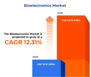
Key Applications in 2026 Healthcare
The integration of electronics into biocompatible substrates has led to a new class of medical devices that were once the domain of science fiction.
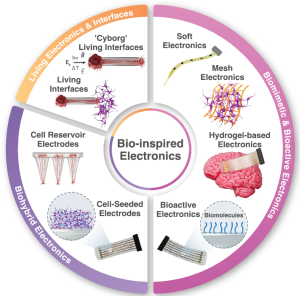 Schematic overview of emerging strategies for bio-inspired electronics and neural interfaces
| Neural Interfaces and “Living Electrodes”. From simple deep brain stimulation, we are moving towards Biohybrid Neural Interfaces that use tissue-engineered axons to bridge the gap between a computer chip and the motor cortex. By “growing” biological wires into the brain, these devices achieve a level of chronic stability that allows paralysed patients to control robotic limbs with the same fluid precision as a biological arm.
Soft Bio-Sensing Wearables: Modern-day wearables have moved from the wrist to the skin. “Electronic skin” (e-skin) patches—ultrathin, breathable, and biocompatible—now monitor biochemical markers in sweat, such as cortisol and glucose, in real-time. These devices utilise MXenes and Graphene to detect molecular changes at concentrations previously only reachable via blood draws. |
| Closed-Loop Bioelectronic Medicine: The concept of “electroceuticals” is now a clinical reality. Small, biocompatible devices implanted on the vagus nerve can monitor inflammatory markers and automatically deliver precise electrical pulses to inhibit the “cytokine storm” associated with autoimmune diseases like rheumatoid arthritis and Crohn’s disease. |
Some key challenges remain to be resolved:
Engineering Challenges:
- Stability and Bio-Integration
Despite the progress, engineering the interface remains a complex task. The physiological environment is incredibly harsh—warm, salty, and chemically active—leading to the degradation of many synthetic materials.
- Hermetic Packaging vs. Biocompatibility
Engineers must find a critical balance between the need to seal sensitive electronics from moisture while ensuring the outer layer is soft enough to integrate with tissue. In 2026, atomic layer deposition (ALD) is used to create nanometer-thin ceramic coatings that provide moisture barriers without adding stiffness.
- The Power Problem
Traditional batteries are bulky and toxic. Next-generation devices are increasingly powered by biofuel cells that harvest energy from blood glucose or through ultrasonic power transfer, which allows deep-seated implants to be recharged wirelessly through layers of muscle and bone
Ethics and the Regulatory Challenges
- As we successfully integrate electronics into the human body, the ethical implications have shifted from “safety” to “agency and privacy.”
- The EU Medical Device Regulation (MDR) and the FDA’s Digital Health Centre of Excellence have established new frameworks for “Neural Data Privacy.”Since these devices can read and potentially influence neural states, the data they produce is classified as a biological asset.
- Furthermore, the longevity of these devices raises questions about “hardware obsolescence” in living patients. Engineering the interface now includes a roadmap for software updates and long-term support for implants that may stay in the body for decades.
The Future: Toward “Living” Bioelectronics
The trend is moving toward synthetic biology-electronics hybrids. We are seeing the prototypes of devices where genetically engineered cells that produce an electrical signal work as “Sensors” when they detect a specific pathogen or cancer marker.
By engineering the interface at the molecular level, we are not just repairing the body; we are enhancing its resilience.
The integration of electronics into biocompatible materials is more than a technical achievement—it is the foundation of a new era of personalised medicine where the device and the patient are the same.
The post Engineering the Interface: Integrating Electronics into Biocompatible Materials for Next-Generation Medical Devices appeared first on ELE Times.
EU–India FTA: A Defining Moment for India’s Electronics and Semiconductor Industry
As global electronics and semiconductor supply chains are restructured for resilience and trust, the proposed EU–India Free Trade Agreement (FTA) is emerging as a pivotal opportunity for the Indian industry. More than a tariff-reduction exercise, the agreement has the potential to integrate India more deeply into Europe’s advanced electronics and semiconductor value chains. For India, the FTA represents a transition—from cost-driven manufacturing to value-driven, technology-led partnership.
The European Union is one of the world’s most quality-conscious electronics markets, with strong demand across automotive electronics, industrial automation, medical devices, power electronics, renewable energy systems, and telecom infrastructure. Under the EU–India FTA, reduced tariffs and streamlined regulatory frameworks will enhance the competitiveness of Indian electronics products.
Alignment on conformity assessment and technical standards will shorten qualification cycles and lower compliance costs, enabling Indian manufacturers to integrate directly into EU OEM and Tier-1 supply chains. As European companies pursue China-plus-one sourcing strategies, India stands to gain as a reliable and scalable manufacturing base.
India’s electronics industry has historically been assembly-led, but this is changing rapidly. Supported by policy incentives and growing design capabilities, Indian firms are expanding into PCB assembly, system integration, testing, and engineering services.
The EU–India FTA accelerates this shift by encouraging European OEMs to localise higher-value activities in India. Electronics manufacturing services (EMS) providers, component manufacturers, and design-led companies can leverage European partnerships to move beyond box build toward design-for-manufacturing, reliability engineering, and lifecycle management—key to long-term competitiveness.
Semiconductors are central to the EU–India technology partnership. The FTA aligns closely with India’s Semiconductor Mission and the EU Chips Act, creating a stable framework for collaboration across design, packaging, testing, and advanced manufacturing.
India’s strengths in chip design, embedded systems, and engineering talent complement Europe’s leadership in semiconductor equipment, materials, power electronics, and automotive-grade chips. Reduced barriers for capital equipment, technology transfer, and skilled workforce mobility can accelerate joint investments in OSAT, ATMP, and speciality semiconductor manufacturing.
This collaboration positions India as a trusted node in Europe’s semiconductor supply chain diversification efforts.
Beyond large fabs and design houses, the FTA creates opportunities for component and equipment suppliers. Demand for sensors, power modules, passive components, connectors, precision tooling, and clean-room equipment is expected to rise as European electronics and semiconductor companies expand operations in India.
Indian MSMEs operating in these segments can integrate into European Tier-2 and Tier-3 supply chains, benefiting from long-term sourcing contracts, technology upgrades, and exposure to global quality benchmarks.
The EU–India FTA also strengthens innovation linkages. Indian start-ups working in semiconductor IP, AI-enabled hardware, EV electronics, power electronics, and Industry 4.0 solutions will gain improved access to European R&D ecosystems, pilot customers, and funding platforms.
Europe’s strong IP regimes and industrial testbeds offer Indian deep-tech start-ups a credible pathway from development to global commercialisation.
Alignment with European technical, safety, and environmental standards will enhance the global credibility of Indian electronics and semiconductor products. Standards convergence reduces certification duplication, improves supplier trust, and increases acceptance across multiple export markets. For global buyers, this translates into confidence in Indian suppliers—an essential requirement in electronics and semiconductor sourcing.
The EU–India FTA arrives at a defining moment for the electronics and semiconductor industry. With effective execution, it can accelerate India’s shift from assembly-led operations to value-added manufacturing, design, and innovation. More importantly, it positions India as a strategic, trusted partner in global electronics and semiconductor supply chains—built on quality, resilience, and long-term collaboration.
Devendra Kumar
Editor
The post EU–India FTA: A Defining Moment for India’s Electronics and Semiconductor Industry appeared first on ELE Times.
Future-Proofing Bharat: India’s Multi-Billion Dollar AI Strategy Revealed
India is hosting the AI Impact Summit 2026 under the Ministry of Electronics and Information Technology, this month from February 16-20. The Summit has received a phenomenal response from across the world, and is shaping up to be the biggest such event so far globally, said Union Minister Ashwini Vaishnaw on Friday.
The summit week will feature around 500 curated events across Bharat Mandapam and Sushma Swaraj Bhawan. The AI Impact Expo will host over 840 exhibitors, including country pavilions, Ministries, State governments, industry, start-ups, and research institutions, showcasing AI solutions with proven real-world impact.
The conference has confirmed the participation of 15 Heads of State Government, more than 40 Ministers, over 100 leading CEOs and CXOs, and more than 100 eminent academics. Industry partners, including Jio, Qualcomm, OpenAI, Nvidia, Google, Microsoft, Adobe, and the Gates Foundation, are expected to participate in the event.
The Minister also informed that leading IT companies had developed over 200 focused and sector-specific AI models, expected to be launched during the upcoming summit. With investments worth nearly $70 billion already flowing into the AI infrastructure layer, the potential to double it by the conclusion of the event is exponential, he added. The AI talent pool is expected to be scaled up by extending infrastructure and industry-finalised curricula to 500 universities.
Budget Highlights for the AI Sector
Additionally, the government has proposed to focus on developing the AI landscape in India with specific provisions in the Union Budget 2026-27. As the focus shifts to building the digital infrastructure, the government has proposed an additional investment of USD 90 billion, specifically for the AI Data Centres and further encouraged long-term investments by proposing a tax holiday till 2047 for foreign companies providing cloud services to customers globally using data centre services from India. Such companies will provide services to Indian customers through an Indian reseller entity. Simultaneously, a safe harbour of 15 per cent on cost has also been proposed where the data centre service provider in India is a related entity.
The government has proposed several domains for AI integration in the Indian landscape: –
- Governance: Serving as a force multiplier for improved public service delivery.
- Supporting new technologies: Adopting new technologies in various sectors through the AI Mission and National Quantum Mission.
- Labour market analysis: Assessing the impact of emerging tech such as AI on job roles and skill requirements.
- Bharat-VISTAAR: A new multilingual AI tool designed for broader linguistic accessibility.
- Agriculture: Integration with AgriStack portals and ICAR agricultural practice packages.
- Healthcare & accessibility: R&D and integration into assistive devices for People with Disabilities manufactured by Artificial Limbs Manufacturing Corporation of India (ALIMCO).
- Customs & security: Expanding non-intrusive scanning and advanced imaging for risk assessment.
- Education: Embedding AI modules directly into the national education curriculum from school level onwards and for teacher training.
- Professional development: Upskilling and reskilling programs for engineers and tech professionals.
- Employment matching: AI-enabled platforms to connect workers with jobs and training opportunities.
India’s AI Landscape
Since 2020, the Artificial Intelligence (AI) start-up ecosystem in India has experienced rapid growth, with over 150 native AI start-ups having raised over $1.5 billion in funding as of September 2025.
As of early 2026, there are over 1,900 total AI companies in India, with 555 being funded. AI start-ups have touched several industries to provide a technically advanced perspective to the workings in the industry, from healthcare, agriculture, Aerospace & Defence, navigation, to education, manufacturing, banking, and E-commerce. Some notable start-ups include Sarvam AI, Krutrim, Observe.AI, Avaamo, Nanonets, and Atomicwork in the sector.
Global giants like IBM, Google, Microsoft, OpenAI, and Nvidia have established or expanded their R&D centres, engineering hubs, and regional offices in India to leverage the country’s vast tech talent pool and rapidly expanding digital economy. Domestic players like Perplexity has partners with telecom giants like Airtel to expand their reach. Simultaneously, Anthropic, the AI start-up backed by Google and Amazon, plans to open its first Indian office in Bengaluru in early 2026, focusing on AI tools and tapping into the local developer ecosystem.
Future of AI in India
The AI market is projected to reach $126 billion by 2030, with a long-term contribution of $1.7 trillion to India’s GDP by 2035.
These developments, coupled with the government’s initiative to boost the sector and focus on “Sovereign AI” to reduce dependency on foreign technology and build custom chips within 3-5 years, can position India as a formidable force in the sector of Artificial Intelligence globally, while the country already ranks third globally in AI competitiveness.
By: Shreya Bansal, Sub-Editor
The post Future-Proofing Bharat: India’s Multi-Billion Dollar AI Strategy Revealed appeared first on ELE Times.
Budget 2026-27: India Semiconductor Mission 2.0 Announced to Boost 3 nm & 2 nm technology nodes in India
The Union Budget 2026-27 outlines the continuation of India’s deep commitment to the domestic semiconductor ecosystem, aiming to promote it to new heights. Union Finance Minister Smt Nirmala Sitharaman, in the Union Budget 2026-27, announces the launch of India Semiconductor Mission 2.0 (ISM 2.0). It will be a continuation of the earlier ISM 1.0 with a realigned goal to produce equipment and materials, design full-stack India IP, and solidify supply chains, a milestone for the technology sector. ‘This time the mission carries a broad mandate to enable the next level of India’s electronic stride into products and more IPs, precisely.
“ISM 1.0 expanded India’s semiconductor sector capabilities. Building on this, we will launch ISM 2.0 to produce equipment and materials, design full‑stack Indian IP, and fortify supply chains. We will also focus on industry‑led research and training centres to develop technology and a skilled workforce,” she said.
Upgrading India’s Semiconductor Ecosystem
Shri Ashwini Vaishnaw, Union Minister of Railways, Electronics and Information Technology, said that the Budget has announced the launch of India Semiconductor Mission (ISM) 2.0, building upon the strong foundation created under ISM 1.0, which established a completely new and foundational semiconductor industry in India.
ISM 2.0 will focus on designing and manufacturing semiconductor equipment in India, manufacturing of materials used in semiconductor production, creation of a large design ecosystem, and further strengthening of talent development initiatives. A provision of Rs. 1,000 crore has been made for ISM 2.0 for FY 2026-27.
Support for Fabless Startups
The mission launch finds mention in the Budget 2026-27 with a fresh outlay of ₹1,000 crore allocation in the BE fiscal 2027. Vaishnaw said recently that the government plans to support at least 50 fabless chip companies in ISM 2.0 by scaling up the Design Linked Incentive Scheme, with the long-term goal of producing “one AMD” and “one Qualcomm” from India.
“The Union Budget 2026–27 charts a decisive course for India’s evolution into a global technology leader. The enhanced capital outlay of ₹12.2 lakh crore and the launch of the India Semiconductor Mission 2.0 reaffirm the government’s commitment to deep-tech indigenization,” says Mr. Meenu Singhal, Regional Managing Director, Socomec Innovative Power Solutions.
Talking about the budget Mr Pankaj Mohindroo, Chairman, ICEA, says, “Budget 2026–27 reinforces the government’s commitment to manufacturing-led growth, particularly in electronics and semiconductors, through continuity, scale, and targeted reforms. Measures such as the expansion of ECMS, support for ISM 2.0, and long-term incentives for cloud and data infrastructure send a strong signal of strategic intent and policy stability.
The post Budget 2026-27: India Semiconductor Mission 2.0 Announced to Boost 3 nm & 2 nm technology nodes in India appeared first on ELE Times.
Caliber Interconnects Achieves ARAI Certification for EV Charging Solutions, Strengthening India’s Indigenous EV Infrastructure
Caliber Interconnects Private Ltd., a leading Indian engineering and deep-tech solutions company, today announced that its electric vehicle (EV) charging portfolio has been awarded ARAI certification, marking a significant milestone in the company’s journey to deliver reliable, safe, and future-ready charging infrastructure for India’s rapidly evolving mobility ecosystem.
The certification from the Automotive Research Association of India (ARAI) validates Caliber’s adherence to stringent national standards for safety, performance, and environmental compliance—benchmarks critical to the Indian automotive and EV industries.
“This milestone goes far beyond a certificate—it’s a clear signal of our engineering depth and long-term commitment to India’s EV future,” said Suresh Babu, Founder & CEO, Caliber Interconnects. “ARAI certification reinforces our belief that India deserves globally competitive EV charging solutions that are designed, manufactured, and supported locally. At Caliber, we are building high-performance charging systems that the ecosystem can depend on—not just today, but for the decade ahead.”
A Comprehensive, ARAI-Certified EV Charging Portfolio
Caliber Interconnects offers one of the industry’s most versatile EV charging portfolios, addressing residential, commercial, fleet, and public charging needs:
- AC Chargers: 3.3 kW | 7.4 kW | 22 kW
- Hybrid Chargers: 30 kW DC + 22 kW AC
- DC Fast Chargers: 30 kW | 60 kW | 120 kW | 240 kW
- Two-Wheeler DC Chargers: 3 kW | 6 kW
All chargers are powered by Cogency, Caliber’s intelligent smart-charging platform engineered for real-time monitoring, predictive maintenance, and optimized charger performance.
Intelligent, Scalable, and Standards-Compliant
Cogency is OCPP 1.6 and 2.0.1 compliant and supports both Android and iOS, enabling seamless system integration, remote management, and scalable deployments across diverse charging networks. The platform is designed to meet the operational demands of utilities, charge point operators, OEMs, and infrastructure developers.
With ARAI certification, Caliber’s EV chargers meet the highest standards expected by India’s automotive industry—ensuring safety, durability, and environmental responsibility across operating conditions.
Designed in India. Built for Scale.
At a time when the market is saturated with imported EV chargers, Caliber Interconnects is championing locally manufactured, future-ready solutions that reduce dependency, improve serviceability, and strengthen India’s EV value chain.
Whether supporting immediate deployments or long-term infrastructure planning, Caliber’s charging solutions are engineered to scale alongside the growing demands of India’s EV and clean-energy ecosystem.
The post Caliber Interconnects Achieves ARAI Certification for EV Charging Solutions, Strengthening India’s Indigenous EV Infrastructure appeared first on ELE Times.
ICEA Welcomes Budget 2026–27’s Focus on Manufacturing, Flags Key Structural Gaps
India Cellular and Electronics Association (ICEA) said that the Union Budget 2026–27 adopts a steady and largely inclusive approach, reinforcing India’s manufacturing and technology ecosystem through policy continuity, scale, and targeted reforms.
The sustained focus on electronics manufacturing, the launch of India Semiconductor Mission (ISM) 2.0, and the significant expansion of the Electronics Component Manufacturing Scheme (ECMS) reaffirm the government’s long-term commitment to building resilient domestic supply chains and strengthening India’s position in global value chains.
ICEA also welcomed the announcement of a tax holiday till 2047 for foreign companies offering global cloud services using India-based data centres, describing it as a forward-looking measure that provides long-term policy certainty, anchors global digital infrastructure in India, and enhances the country’s credibility as a trusted hub for data, cloud, and AI-led services. Long-term predictability, as provided in this measure, will be a sure win for our nation.
Additional measures, such as the five-year income tax exemption for foreign suppliers of capital equipment in bonded zones, the Safe Harbour framework for non-resident component warehousing, customs decriminalisation, and extended validity of advance rulings, are expected to improve ease of doing business, reduce compliance friction, and strengthen investor confidence.
However, ICEA noted that there are a few unfinished businesses. Inverted duty structures across capital equipment, display assemblies, inductors, FPCA, MICs, receivers, speakers, and specialised inputs continue to impact cost competitiveness. Partial progress on MOOWR reforms, limited clarity on tax-neutral VMI models, and residual uncertainty around Permanent Establishment (PE) exposure for foreign-owned capital equipment remain constraints to faster scale-up.
Commenting on the Budget, Mr. Pankaj Mohindroo, Chairman, ICEA, said: “Budget 2026–27 reinforces the government’s commitment to manufacturing-led growth, particularly in electronics and semiconductors, through continuity, scale, and targeted reforms. Measures such as the expansion of ECMS, support for ISM 2.0, and long-term incentives for cloud and data infrastructure send a strong signal of strategic intent and policy stability.
“At the same time, key structural issues, especially inverted duty structures, unfinished MOOWR reforms, and tax-related uncertainties, need timely resolution to ensure cost competitiveness and speed of execution,” Mr. Mohindroo added.
ICEA Chairman further stated that the exponential growth in mobile manufacturing has clearly demonstrated what bold and consistent policy measures can achieve. “To replicate this success across sectors and move towards 25% of GDP through manufacturing, the National Manufacturing Mission is a need of the nation, enabling the ecosystem to truly fire on all cylinders,” he said.
ICEA reiterated its commitment to working closely with the government and stakeholders to support policy implementation and accelerate India’s journey towards becoming a globally competitive electronics manufacturing hub.
The post ICEA Welcomes Budget 2026–27’s Focus on Manufacturing, Flags Key Structural Gaps appeared first on ELE Times.
Enabling the Road to 6G: How Rohde & Schwarz Is Shaping the Future of Wireless Networks
Senior leaders from Rohde & Schwarz shared their perspectives with Kumar Harshit, Technology Correspondent at ELE Times, on the evolving wireless landscape, discussing the transition from 5G to 6G and the technologies shaping next-generation networks. The conversation focused on rising network complexity and the growing importance of intelligent test and measurement solutions.
The conversation was enriched by insights from Simon Ng, Sales Director – Mobile Network Testing (Asia Pacific), R&S Regional Headquarters, Singapore; Alexander Pabst, Vice President – Market Segment Wireless Communication, R&S GmbH & Co. KG, Germany; and Mahesh Basavaraju, Market Segment Manager – Wireless Communication, R&S India Pvt. Ltd.
Together, the leaders shared a cohesive outlook on key enablers of future networks, including advanced test and measurement methodologies, AI-native and AI-assisted networks, non-terrestrial and satellite integration, the emergence of Wi-Fi 8, and India’s expanding role as a critical hub for telecom R&D and innovation.
Here are the excerpts from the conversation:
ELE Times: How does Rohde & Schwarz view localization, particularly in manufacturing and equipment development in India?
R&S: Rohde & Schwarz develops global technologies for a global market. Rather than localizing products in isolation, we operate through a unified global development model. India plays a key role in this framework.
We have over 200 engineers in India who contribute directly to our global R&D efforts. The solutions developed through this collaboration are deployed worldwide, including in India. In that sense, India is deeply integrated into our global innovation ecosystem.
ELE Times: As the industry transitions from 5G toward 6G, how is Rohde & Schwarz positioning itself?
R&S: Connectivity is no longer limited to consumer communication; it is becoming core infrastructure for industry and society. While 5G has enabled private networks, industrial IoT, and enterprise use cases, 6G will take this further.
With 6G, we expect higher operating frequencies, native integration of non-terrestrial networks such as satellites, network sensing capabilities, and deeper convergence of AI, XR, and communication technologies. Our role is to enable this entire ecosystem—on both the network and device sides—through advanced test, measurement, and validation solutions, from early research to commercialization.
ELE Times: What are the defining technology pillars you associate with 6G?
R&S: Three pillars stand out clearly. First is ubiquitous connectivity, where satellite communication becomes a native part of the network rather than an add-on. Second is immersive and intelligent experiences driven by the convergence of XR, AI, and sensing technologies. Third is energy and spectrum efficiency, which will be critical to ensure sustainability as network capacity and complexity continue to grow.
ELE Times: Rohde & Schwarz is known for working in the pre-market phase. How early are you involved in new technology development?
R&S: Very early. Typically, we operate three to five years ahead of commercial deployment. Our responsibility is to translate high-level visions—such as holographic communication or pervasive sensing—into concrete, testable technical requirements.
This includes supporting evolving standards, advances in massive MIMO, AI-driven air interfaces, integrated sensing and communication (ISAC), and next-generation antenna systems. We work closely with industry players to ensure these technologies are testable and reliable long before they reach the market.
ELE Times: Wi-Fi 8 is emerging alongside cellular evolution. Why is Wi-Fi 8 important?
R&S: Wi-Fi 8 is less about peak data rates and more about reliability, coordination, and scalability. One key improvement is the ability of access points to coordinate spectrum usage among themselves, significantly reducing interference.
It also enhances mesh networking, improves spectrum efficiency, and allows a single cell to serve more users reliably. While there may be incremental increases in bandwidth, the real value lies in better-managed spectrum and consistent user experience.
ELE Times: Can you highlight some recent breakthroughs in test and measurement technologies?
R&S: One important area is testing XR and AI applications over wireless networks. Unlike wired connections, wireless networks introduce latency, fading, congestion, and other impairments that directly affect performance. Our platforms can simulate these real-world conditions to validate application behavior accurately.
Another breakthrough is in base station testing. Traditionally, this required large racks of individual instruments. We have introduced compact, fully integrated base station testers that are cost-efficient, reliable, and well-suited for production environments.
We have also developed solutions for millimeter-wave Wi-Fi, particularly relevant to India, and advanced test setups for non-terrestrial networks, including satellite-based communication.
ELE Times: How do you assess India’s progress after its rapid nationwide 5G rollout?
R&S: India’s progress has been remarkable. Network quality, coverage, and speed have improved dramatically in a short time. More importantly, India is no longer content with being a fast follower.
There is a strong national ambition to be at the forefront of 6G, supported by government funding, research programs, and industry collaboration. We are actively supporting this journey by working closely with Indian operators, OEMs, startups, and academic institutions.
ELE Times: What role does Rohde & Schwarz play in India’s 6G and R&D ecosystem?
R&S: We are actively engaged with the Bharat 6G Alliance and contribute across multiple working groups covering technology, spectrum, and use cases. Our role is to bring global experience into Indian research programs and testbeds.
India has set ambitious goals around creating domestic intellectual property for 6G. We already see strong innovation emerging from Indian universities and startups, particularly in areas such as massive MIMO and AI-driven networks, and we support them with advanced validation and measurement platforms.
ELE Times: What are the key challenges in pre-silicon testing and validation?
R&S: One major challenge has been early-stage testing. Historically, this required complex hardware simulators and tightly synchronized physical interfaces. We have now shifted toward software-based testing using IQ-over-IP, enabling validation at a much earlier stage.
Another important shift is continuous integration, where software can be repeatedly tested in pre-silicon environments before being committed to hardware. This significantly accelerates development cycles.
We are also simplifying automation by moving from traditional programming approaches to Python-based workflows and introducing AI-assisted scripting, allowing engineers to define complex tests using natural language.
ELE Times: AI is becoming central to telecom systems. How does Rohde & Schwarz approach AI?
R&S: From a telecom perspective, AI can be broadly categorized into AI on RAN, AI for RAN, and AI and RAN. Our primary focus is AI for RAN, where AI is used to optimize network performance.
AI introduces many new variables, making performance validation more complex. Our focus is on enabling fair, repeatable, and meaningful testing. Internally, we see AI as a powerful enabler rather than a replacement for engineers. The engineer remains at the center of decision-making, with AI enhancing efficiency, automation, and insight.
ELE Times: Finally, how do you see India shaping the global 6G ecosystem?
R&S: India brings together scale, talent, a vibrant startup ecosystem, and strong policy support. What is particularly striking is the density of innovation and risk-taking startups, supported by government initiatives.
With sustained investment in research, testbeds, and global collaboration, India is well-positioned to influence global 6G standards and deployments. We expect India to play a significant role in shaping the future of wireless communication worldwide.
The post Enabling the Road to 6G: How Rohde & Schwarz Is Shaping the Future of Wireless Networks appeared first on ELE Times.
Union Budget 2026-27: ECMS Gets a budgetary Outlay of Rs 40,000 Crore, Big boost to Components Manufacturers in India
The Union Budget 2026-27 presented in the parliament on 1st February, 2026, allocates Rs 40, 000 crore to the Electronics Components Manufacturing Scheme (ECMS) launched last year in April. With a proposed budgetary outlay of around Rs 40,000 Crore for the Electronics Components & Manufacturing Scheme (ECMS), as compared to the previous outlay of Rs 22,919 crore during its launch in April 2025, the government intends to ensure that India’s electronics components game goes up globally. The outlay is being doubled even as the scheme “already has investment commitments at double the target,” and the near-doubling of the outlay will “capitalise on the momentum,” she says.
The increased budgetary outlay will highly benefit the electronics sector in India as it aims to promote the domestic manufacturing of electronics components that the nation really needs at this time, so as to become the real electronics hub globally. It promotes the manufacturing of Printed Circuit Boards (PCBs), lithium-ion Cells and other necessary electronics components used in modern-day devices ranging from mobile phones to automobiles.
Commitment to Mnaufacturing-led Growth
Commenting on the Budget, Mr. Pankaj Mohindroo, Chairman, ICEA, says, “Budget 2026–27 reinforces the government’s commitment to manufacturing-led growth, particularly in electronics and semiconductors, through continuity, scale, and targeted reforms.”India Cellular & Electronics Association (ICEA) is India’s apex industry body representing the entire mobile and electronics ecosystem. “Measures such as the expansion of ECMS, support for ISM 2.0, and long-term incentives for cloud and data infrastructure send a strong signal of strategic intent and policy stability,” he adds.
The EMS Component in GDP to Increase
The intent behind the budgetary outlay speaks volumes about the government’s vision for the electronics industry. Talking about this very thing, Mr Jasbir Singh, Executive Chairman and CEO, Amber Enterprises, welcomes the governmnet’s decision to increase the budgetary outlay. He says,” Cementing this further, the decision to establish high-tech tool rooms to manufacture high-precision components at scale and lower cost will propel India to become self-reliant and globally competitive.”
He also commends the government’s decision to rejuvenate 200 legacy industrial clusters, which will boost the EMS sector tonexponential growth. He adds,” These policies will increase the EMS contribution to the GDP, expected to be the third-largest.”
A Mighty Scheme
The scheme has approved 46 projects so far, attracting cumulative investments of ₹54,567 crore, with projected production valued at ₹3.68 trillion and the creation of over 50,000 direct jobs. Notified with a six-year budgetary outlay of ₹22,919 crore, the scheme envisages a total production of ₹10.34 lakh crore and employment generation for nearly 142,000 people. It is designed to lay the groundwork for a $500-billion electronics manufacturing ecosystem by 2030–31.
The post Union Budget 2026-27: ECMS Gets a budgetary Outlay of Rs 40,000 Crore, Big boost to Components Manufacturers in India appeared first on ELE Times.
Microchip Expands its Arm Cortex-M0+ Portfolio with PIC32CM PL10 MCUs
Building on decades of experience in serving embedded applications where low power, affordability and ease of development are critical, Microchip Technology has added PIC32CM PL10 MCUs to its PIC32C family of Arm Cortex-M0+ core devices. PL10 MCUs feature a rich set of Core Independent Peripherals (CIPs), 5V operation, touch capabilities, integrated toolsets and safety compliance. The device family targets high-volume applications including industrial control, building automation, consumer appliances, power tools and sensor-based systems. As part of the company’s unified MCU strategy, PL10 devices offer pin-to-pin compatibility with AVR MCUs.
The integrated Peripheral Touch Controller (PTC), along with a 12-bit Analogue-to-Digital Converter (ADC) are designed to provide responsive performance in touch applications and strong noise immunity for analogue signal measurement. Additional on-chip CIPs help offload time-critical, repetitive and deterministic tasks from the CPU to improve real-time performance and power efficiency. The PL10 supports the Cortex Microcontroller Software Interface Standard (CMSIS), enabling the development of modular, reusable application code to accelerate the process.
In addition to support from Microchip’s MPLAB development ecosystem, the PL10 family incorporates industry-standard tools and integrated development environments (IDEs), providing developers with more flexibility in how they build, debug, and deploy their software. Compatible third-party tools include Microsoft Visual Studio Code (VS Code), IAR Systems, Arm Keil, SEGGER, Zephyr and MikroElektronika. AI-driven resources such as the MPLAB AI Coding Assistant offer context-aware code generation and real-time product insights to help accelerate and simplify development.
“PL10 MCUs help engineers more easily migrate to higher performance microcontrollers while maintaining the straightforward development experience, power efficiency and cost structure of our established 8-bit solutions,” said Greg Robinson, corporate vice president of Microchip’s MCU business unit. “As we prepare to introduce a range of new microcontrollers over the next 12-18 months, with everything spanning entry-level to AI-capable devices, Microchip is strengthening its commitment to a comprehensive MCU portfolio designed to meet evolving market demands.”
The PL10 family is designed to comply with various industry safety standards, including International Organisation for Standardisation (ISO) 26262 for functional safety in electrical and electronic systems of road vehicles. Additionally, the MCUs are designed to operate from 1.8 to 5.5 volts, supporting performance in high-noise environments such as automotive, IoT, industrial automation and consumer electronics applications. PL10 MCUs enable simultaneous connection to devices operating at different voltage levels without external level shifters using the integrated Multi-Voltage I/O (MVIO).
The post Microchip Expands its Arm Cortex-M0+ Portfolio with PIC32CM PL10 MCUs appeared first on ELE Times.
Vishay Intertechnology’s 1200 V SiC MOSFET Power Modules for Power Efficiency
Vishay Intertechnology, Inc. has introduced five new 1200 V MOSFET power modules designed to increase power efficiency for medium to high frequency applications in automotive, energy, industrial, and telecom systems. The Vishay Semiconductors VS-SF50LA120, VS-SF50SA120, VS-SF100SA120, VS-SF150SA120, and VS-SF200SA120 feature Vishay’s latest generation silicon carbide (SiC) MOSFETs in the industry-standard SOT-227 package.
Offered in single switch and low side chopper configurations, each power module released today features a SiC MOSFET integrated with a soft body diode offering low reverse recovery. The result is reduced switching losses and increased efficiency for solar inverters, off-board chargers for electric vehicles (EV), SMPS, DC/DC converters, UPS, and HVAC systems; large-scale battery storage systems, and telecom power supplies.
The compact SOT-227 package of the VS-SF50LA120, VS-SF50SA120, VS-SF100SA120, VS-SF150SA120, and VS-SF200SA120 allows the devices to serve as drop-in replacements for competing solutions in existing designs, enabling designers to adopt one of the newest SiC technologies without the expense of changing PCB layouts. The moulded package also offers electrical insulation up to 2500 V for one minute, lowering costs by eliminating the need for additional insulation between the component and heatsink.
The power modules provide continuous drain current from 50 A to 200 A and low on-resistance down to 12.1 mΩ. The RoHS-compliant devices deliver high-speed switching with low capacitance and offer a high maximum operating junction temperature of +175 °C.
Device Specification Table:
|
Part # |
VDSS |
ID |
RDS(ON) |
Configuration |
Package |
|
VS-SF50LA120 |
1200 V |
50 A |
43 mΩ |
Low side chopper |
SOT-227 |
|
VS-SF50SA120 |
50 A |
47 mΩ |
Single switch |
||
|
VS-SF100SA120 |
100 A |
23 mΩ |
Single switch |
||
|
VS-SF150SA120 |
150 A |
16.8 mΩ |
Single switch |
||
|
VS-SF200SA120 |
200 A |
12.1 mΩ |
Single switch |
Samples and production quantities of the VS-SF50LA120, VS-SF50SA120, VS-SF100SA120, VS-SF150SA120, and VS-SF200SA120 are available now, with lead times of 13 weeks.
The post Vishay Intertechnology’s 1200 V SiC MOSFET Power Modules for Power Efficiency appeared first on ELE Times.
Budget 2026-27: Can New PLI Schemes Drive India’s A&D Tech Sovereignty?
As the Union Budget approaches, the spotlight intensifies on India’s aerospace and defence technology sector, a vertical that has transitioned from a heavy importer to a nascent global manufacturing hub. The numbers tell a story of aggressive scaling: under the aegis of “Atmanirbhar Bharat,” domestic defence production surged to a historic ₹1.27 lakh crore in FY 2023-24.
However, for an industry eyeing a $5 trillion economy, this record high is viewed not as a finish line, but as a baseline. The shift toward indigenous manufacturing has fundamentally rewired the nation’s military-industrial complex, replacing foreign dependency with homegrown R&D and high-tech sovereignty. As the government prepares to lay out its fiscal roadmap, the industry is looking for more than just procurement orders; it is looking for deep-tech incentives, streamlined export pathways, and sustained capital outlay.
This budget will be a litmus test for India’s self-reliance commitment. Stakeholders are bracing for announcements that could further catalyse the aerospace ecosystem, ensuring that “Made in India” weaponry and avionics don’t just meet internal security needs but become a cornerstone of India’s global economic footprint.
The Tech-Sovereignty Mandate
As the lines between commercial innovation and battlefield superiority blur, technology has emerged as the definitive fulcrum for India’s tri-service modernisation. Industry experts argue that the upcoming Budget presents a pivotal window to institutionalise this convergence through aggressive structural reforms.
Central to this discourse is the evolution of the Production Linked Incentive (PLI) Scheme. While the current framework has provided a vital tailwind for the drone industry, there is a growing consensus that a “narrow-lens” approach is no longer sufficient. To truly insulate India’s supply chain from global volatility, the PLI umbrella must expand to cover the high-stakes world of dual-use technologies.
In terms of using technology in aerospace and defence technology development, the use of AI and related features will play a significant role.
“Investing in digital twins and simulation technology for testing and research in aviation and defence can boost precision and efficiency in the electronic manufacturing industry. Tecknotrove urges the government to prioritize use of digital twin technology in this financial budget. It’s a strategic move that will amplify innovation, save research and development and manufacturing costs, and drive India’s self-reliance in manufacturing. Digital twins aren’t just a trend—they’re a game-changer. With decades of expertise in digital twins for aviation and defence, we have seen this technology helping in at least 30% reduction in costs,” says Payal Gupta, Co-Founder, Director-Business Development, Tecknotrove Systems India Pvt. Ltd.
The strategic roadmap for the FY 2026-27 fiscal cycle should ideally prioritise:
- The Full Drone Spectrum: Moving beyond basic assembly to incentivise the manufacturing of high-endurance propulsion systems and autonomous flight controllers.
- Electronic Warfare & Surveillance: Bringing Airborne Early Warning (AEW) systems, jamming devices, and advanced radar arrays under the incentive net to neutralise import dependencies.
- The Robotics Frontier: Providing fiscal stimulus for indigenous sensors and robotic systems that will define the future of unmanned combat and deep-space communication.
By widening these incentive corridors, the government can transform the “Make in India” initiative from a manufacturing slogan into a high-tech powerhouse, ensuring that the next generation of aerospace sensors and AI-driven robotics are conceived, designed, and built on Indian soil.
By: Shreya Bansal, Sub-Editor
The post Budget 2026-27: Can New PLI Schemes Drive India’s A&D Tech Sovereignty? appeared first on ELE Times.
How to Build a Hacker-Proof Car: Insights from the Auto EV Tech Summit
Speaking at the Auto EV Tech Vision Summit 2025, Suresh D highlights the major cyber vulnerabilities and the corresponding technologies required to enable a safer and more resilient automotive ecosystem.
Since the electronic components in passenger vehicles are set to increase by 20-40 percent, as the recent studies suggest, including infotainment, ADAS, etc, drawing in a lot of sensors in the near future, automobiles are emerging as the new battlefield for cyber developments. Underlining this growing phenomenon, Suresh D, Group CTO, Minda Corporation, CEO, Spark Minda Tech Centre & Board Member, Spark Minda Green Mobility says, “A passenger vehicle is expected to see a 20–40 percent increase—nearly doubling in some cases—over the next two to three years, bringing in a large number of on-board electronic systems. This will significantly increase software content and complexity,” at the Auto EV Tech Vision Summit 2025 held at KTPO, Bengaluru, on November 18–19, 2025.
He further goes on to add that the phenomenon will make Operating Systems and other software indispensable, escalating the security question in automobiles.
Critical Challenges on the way
He says that the new architectural parameter of SDVs, where the distributed architecture is being replaced by controlled or zonal architecture, also poses certain security challenges. Also, as the new vehicles remain entirely connected, as in V-2-V or V-2-I connection, the proximity of cyber risks escalates.
Further, he touches upon the critical challenges that are to be tackled, including phishing, hacking, snooping, malware, etc. He goes on to underline some of the crucial cyberattacks that the automotive industry has seen in the recent past, ranging from CAN spoofing a Jeep Cherokee in 2014 to the latest TESLAMATE attack on Tesla cars in 2025, underlining how the question of cybersecurity becomes more relevant than ever.
Curious Case of SDVs & EVs
As EVs are on the rise across the world, Suresh D highlights how EV expansion and the need for robust charging systems also aggravate the risk. He explains that if a charging station compromises a supplier’s build server, it can be manipulated to tamper with BMS parameters via a compromised internal bus or a malicious charging station.
While for SDVs, potential risk sources he underlines include attack scenarios ranging from unprivileged root access and pivoting through fleet management backends, to compromised third-party apps and poorly protected cryptographic keys.
How to Tackle this?
In the latter part, he touches upon the important steps that can be taken to avoid the potential risks and create a safer and reliable cyber ecosystem for automotives. First among them is the System Architecture approach. He says, “It refers to developing a robust architecture—understanding the OEM’s architecture and aligning the product accordingly.” He sums it up as thinking way ahead of the OEMs. It also includes encryption and decryption of the hardware to ensure that no vulnerability remains open to exploitation.
Further, he also outlines a distinct approach, which is Embedded Edge Solutions, which means solving the problem at the source. It includes several protections, including secure flashing and secure boot. This is done through the plant server of the OEM that generates distinct private keys for each of the units for further authorization.
For SDVs, he highlights a telematics-based approach which consists of 3 layers, namely Layer 1- In-vehicle security, Layer 2- Vehicle Communication Security & Layer 3- The cloud infrastructure. When Internet Protocol is used for communication, it enables whitelisting of the IPs through encryption and decryption through SSL, enabling a better and safer environment.
High Frequency Options: Granting More Immunity
He also underlines how automobiles these days usually come with smart keys or keyless access to the vehicle. While the technology is referred to as Low-Frequency Radio Frequency (LFRF), it is immune to relay attacks. However, the industry is gradually moving towards safer and more reliable options like Bluetooth and Ultra Wide Bandgap (UWB), with high-frequency technology making decoding highly difficult.
He adds that even these technologies are prone to cyberattacks, either at the server level or the device level. Conclusively, some techniques like channel sounding with Bluetooth-based technology have been developed, which are more precise and help make authentication more secure. It offers a turnkey secure foundation, making automobiles reliable and secure.
The post How to Build a Hacker-Proof Car: Insights from the Auto EV Tech Summit appeared first on ELE Times.
Palo Alto Networks Unifies Observability and Security for the AI Era through Chronosphere Acquisition
As enterprises increasingly rely on AI to run digital operations, protect assets, and drive growth, success depends on one critical factor: trusted, high-quality, real-time data. Palo Alto Networks, the global cybersecurity leader, announced the completion of its acquisition of Chronosphere, addressing a core challenge of the AI era: the inability to see and secure the massive data volumes running modern businesses.
Chronosphere, a Leader in the 2025 Gartner Magic Quadrant for Observability Platforms, was purpose-built to handle this scale. While legacy tools break down in cloud-native environments, Chronosphere gives customers deep visibility across their entire digital estate. With this acquisition, Palo Alto Networks is redefining how organisations run at the speed of AI—by enabling customers to gain deep, real-time visibility into their applications, infrastructure, and AI systems — while maintaining strict control over data cost and value.
The planned integration of Palo Alto Networks Cortex AgentiX with Chronosphere’s cloud-native observability platform will allow customers to apply AI agents that can now find and fix security and IT issues automatically—before they impact the customer or the bottom line. AI security without deep observability is blind; this acquisition delivers the essential context across models, prompts, users, and performance to move from manual guessing to autonomous remediation.
Nikesh Arora, Chairman and CEO, Palo Alto Networks:
“Enterprises today are looking for fewer vendors, deeper partnerships, and platforms they can rely on for mission-critical security and operations. Chronosphere accelerates our vision to be the indispensable platform for securing and operating the cloud and AI. We believe that great security starts with deep visibility into all your data, and Chronosphere provides that foundation for our customers.”
Martin Mao, Co-founder and CEO, Chronosphere, is joining Palo Alto Networks as SVP, GM Observability and comments:
“Chronosphere was built to help the world’s most complex digital organisations operate at scale with confidence. Joining Palo Alto Networks allows us to bring AI-era observability to a global audience. Together, we’re delivering a new standard — where observability, security, and AI come together to give organisations control over their most valuable asset: data.”
The Chronosphere Telemetry Pipeline remains available as a standalone solution, enabling organisations to eliminate the ‘data tax’ associated with modern security operations. By acting as an intelligent control layer, the pipeline filters low-value noise to reduce data volumes by 30% or more while requiring 20x less infrastructure than legacy alternatives. This is key to Palo Alto Networks Cortex XSIAM strategy, ensuring customers can scale their security posture—not their spending—as they transition to autonomous, AI-driven operations.
The post Palo Alto Networks Unifies Observability and Security for the AI Era through Chronosphere Acquisition appeared first on ELE Times.
Spectral Engineering and Control Architectures Powering Human-Centric LED Lighting
As technological advancements continue to pursue personalisation & customisation at every level, illumination has also transformed from a need to a customisation. Consequently, the LED industry is moving towards a similar yet prominent stride, making customised and occasion-specific solutions, keeping in consideration the human behaviour and lighting changes across the day. Long seen as the constant and uniform thing, illumination is now being reimagined as something dynamic and customisable.
In the same pursuit, the industry has moved towards enabling Human-Centric Lighting(HCL), where lighting is designed and engineered to emulate natural daylight, ranging from dimming them as the Sun goes down, while brightening up as the day begins. Gradually, illumination is now being designed around human biology, visual comfort, and cognitive performance rather than simple brightness or energy efficiency.
But what lies behind this marvel is hardcore engineering. Technically, the result is made possible by the marvels of spectral engineering & control architectures, wherein the former adjusts the light spectrum while the latter enables the intelligence directing the timing changes of the lighting system. Simultaneously, the dual play brings forth today’s human-centric lighting into real-life examples and is also making them more customised and personalised. This ultimately helps in supporting human circadian rhythms, enhancing well-being, mood, and performance.
To enable these engineered outcomes, embedded sensors, digital drivers, and networked control platforms are integrated into the modern-day LED lights, transforming illumination into a responsive, data-driven infrastructure layer. In combination, spectral engineering and intelligent control systems are reshaping the capabilities of LED lighting, transforming it from a passive utility into a dynamic, precision-engineered tool for enhancing human wellbeing, productivity, and performance.
How is Spectral Power Distribution engineered?
When we talk about LED lights, white light is the first thing that comes to our minds. Although the same is not true scientifically. Surprisingly, LEDs inherently emit blue light and not white. To turn the blue light into white, a Phosphor coating is applied over it. Consequently, the blue light mixes with the phosphor to turn some of the light into green, red & yellow simultaneously. These lights eventually mix to turn white.
Spectral Power Distribution (SPD) is simply the profile of the white colour which is not visible to our naked eyes, and how much of each colour is present in the visible white light. The final light can be controlled by various means, such as the type of phosphor, how thick the phosphor layer is, or by adding extra coloured LEDs (like red or cyan).

Spectral Power Distribution is engineered by carefully mixing different colours of light inside an LED, even though it looks white, so that the light feels right for the human body and mind.
Engineering the Spectral Power Distribution of White LEDs
Often, it is seen that the very same white light is sometimes harsh while sometimes soft- all this is because of various variables. Today, from being a static character, SPD has turned into a tunable design parameter,++ becoming a Controllable Design Variable. To this effect, SPD is largely controlled by Phosphor composition (which colours it emits), Particle size and density, and finally Layer thickness and distribution.
That’s why the same 400K LEDs from different manufacturers can feel completely different — their SPDs are different, even if the Correlated Color Temperature (CCT) is the same. But as long as the final color is decided by some application made during manufacturing, the effect remains static. While spectral Power distribution is essential, it is equally important to dictate the given behaviour as per the time of the day.
Multi-Channel LED Configurations for Spectral Tunability
To enable a real-time nature to this Spectral tunability, engineers today use multiple LED channels, including:
- White + Red
- White + Cyan
- RGBW / RGBA
- Tunable white (warm white + cool white)
By precisely varying the current supplied to each LED channel, the spectral power distribution can be reshaped in real time, allowing the system to shift between blue-enriched and blue-reduced lighting modes as required. This level of control allows you to adjust the perceived colour temperature independently of the light’s biological impact, rather than having them locked together. As a result, SPD is no longer a fixed characteristic of the light source but becomes a dynamic, real-time controllable design parameter.
Melanopic Response, Circadian Metrics, and Spectral Weighting
When we talk about light, visibility & brightness make up the primary issue, but that has changed drastically with the emergence of Human Centric Lighting (HCL). With HCL coming into play, photopic lux, the quantification of brightness, is no longer a go-to metric to decide upon the quality of lighting. It is because it explained only one part of the coin, which is visibility, and not how this light or visibility affects human biology.
At the same time, Human Centered Lighting focuses on how light affects the circadian system, alertness, sleep–wake cycles, mood, and hormonal regulation. This phenomenon has brought up new metrics that tell us not only about the brightness or visibility, but also how it biologically acts. One such metric is Melanopic Lux, which weights the spectrum based on melanopsin sensitivity. Melanopsin is a photopigment in our eyes, usually sensitive to Blue-Cyan light.
Interestingly, more melanopic stimulation → increased alertness and circadian activation, while less melanopic stimulation → relaxation and readiness for sleep. That’s where we come to the core of our subject – Light induced behaviuour. The emergence of Melanopic Lux allows engineers to decouple visual brightness from biological effect, giving the right direction to Human Centric Lighting.
While melanopic metrics define what kind of biological response light should produce, control architectures determine when and how that response is delivered. Translating circadian intent into real-world lighting behaviour requires intelligent control systems capable of dynamically adjusting spectrum, intensity, and timing throughout the day. This is where embedded sensors, digital LED drivers, and networked control platforms come into play, enabling lighting systems to modulate melanopic content in real time—boosting circadian stimulation during the day and reducing it in the evening—without compromising visual comfort or energy efficiency.
Other metrics, such as Melanopic Equivalent Daylight Illuminance (EDI) and Circadian Stimulus (CS) are used to quantify how effectively a light source supports circadian activation or melatonin suppression, beyond what photopic lux can describe.
LED Drivers and Power Electronics for Dynamic Spectral Control
In human-centric lighting systems, LED drivers are no longer simple power supplies but precision control elements that translate circadian intent into real-world illumination. Because LEDs are current-driven devices, accurate current regulation is essential to maintain stable brightness and spectral output, especially as temperature and operating conditions change.

Dynamic spectral tuning typically relies on multi-channel LED architectures, making channel balancing a critical requirement. Each LED colour behaves differently electrically and thermally, and without independent, well-balanced current control, the intended spectral profile can drift over time, affecting both visual quality and biological impact.
Equally important is dimming accuracy. Human-centric lighting demands smooth, flicker-free dimming that preserves spectral integrity at all brightness levels, particularly during low-light, evening scenarios. Advanced driver designs enable fine-grained dimming and seamless transitions, allowing lighting systems to dynamically adjust spectrum and intensity throughout the day while maintaining visual comfort and circadian alignment.
System Integration Challenges and Design Trade-Offs
While human-centric lighting promises precise control over both visual and biological responses, delivering this in real-world systems involves significant integration challenges and design trade-offs. Spectral accuracy, electrical efficiency, thermal management, and system cost must all be balanced within tight form-factor and reliability constraints. Multi-channel LED engines increase optical and control complexity, while higher channel counts demand more sophisticated drivers, sensing, and calibration strategies.
Thermal effects further complicate integration, as LED junction temperature directly influences efficiency, colour stability, and lifetime. Without careful thermal design and feedback control, even well-engineered spectral profiles can drift over time. At the same time, adding sensors, networking, and intelligence introduces latency, interoperability, and cybersecurity considerations that must be addressed at the system level.
Ultimately, successful human-centric lighting solutions are defined not by any single component, but by holistic co-design—where optics, power electronics, controls, and circadian metrics are engineered together. The trade-offs made at each layer determine whether a system merely adjusts colour temperature or truly delivers biologically meaningful, reliable, and scalable lighting performance.
The post Spectral Engineering and Control Architectures Powering Human-Centric LED Lighting appeared first on ELE Times.
Pages

