
ELE Times

ASDC Advocates for 2 Lakh Skilled Professionals by 2030 to Power EV Revolution
New Delhi: Automotive Skills Development Council (ASDC) made a strong showing at the Bharat Mobility Global Auto Expo 2025, India’s premier automotive event, with prominent displays at Bharat Mandapam in New Delhi. The stalls, inaugurated by ASDC’s President F R Singhvi, aimed to showcase the council’s crucial skilling initiatives and underscore the importance of attracting young talent to the automotive sector.
Speaking at the expo, F R Singhvi, who also serves as JMD of Sansera Engineering Pvt Ltd, emphasized the event’s alignment with Prime Minister Narendra Modi’s vision for a greener India, focusing on advanced energy storage, green hydrogen, and e-mobility. “The battery is the core of this industry,” Singhvi stated, citing the India Battery Manufacturing Vision, which projects over 2.6 million jobs and a USD 35 billion investment by 2035. He further highlighted the rapid growth of EV sales as a cleaner alternative and reiterated the government’s ambitious goal of 30% vehicle fleet electrification by 2030.
Singhvi highlighted the surging adoption of electric vehicles (EVs) in India, propelled by the government’s ambitious target of 30% fleet electrification by 2030. “Achieving 100% localization of EV components will require adding 30,000 EV-ready workers annually,” he said. By 2030, the automotive sector will need up to 2 lakh skilled professionals to support this transformative vision. He added, “The auto industry’s biggest challenge lies in addressing the shortage of skilled manpower equipped for the electric vehicle sector.”
Vinkesh Gulati, Vice President, ASDC, forecasted substantial growth in India’s domestic EV market, stressing the need for rapid upskilling, reskilling, and fresh skilling to keep pace with global trends. “The transition from Internal Combustion Engine (ICE) vehicles to EVs demands expertise across multiple disciplines, including electrical, mechanical, chemical, and electronics engineering,” Gulati explained. He pointed out that technical overlaps between ICE and EV technologies are minimal, necessitating targeted training programs for existing and new talent pools.
Arindam Lahiri, CEO, ASDC reiterated the stalls’ purpose: showcasing the importance of skilling for the EV industry and attracting young professionals. He emphasized the need for industry outreach to academic institutions and participation in expos to expose students to the exciting opportunities within the automotive sector. ASDC is committed to bridging the industry-academia gap through faculty involvement in industry experiences and regular student interactions. The stalls highlighted various skilling initiatives and programs designed to address skill gaps within the industry.
ASDC also set up a stall at the Yashobhoomi Convention Centre in Dwarka, New Delhi, showcasing its skilling initiatives. The council highlighted the critical role of hiring assessed and certified professionals to enhance talent retention and mitigate skill mismatches during recruitment. Expo attendees were invited to explore the stall to gain insights into ASDC’s programs, with a call to stakeholders to collaborate in addressing the skill gaps within the automotive industry.
The post ASDC Advocates for 2 Lakh Skilled Professionals by 2030 to Power EV Revolution appeared first on ELE Times.
Infineon and the BSI pave the way for a quantum-resilient future: World’s first Common Criteria Certification for post-quantum cryptography algorithm on a security controller
- Infineon receives world’s first Common Criteria EAL6 certification for implementing a post-quantum cryptography (PQC) algorithm in a security controller
- Internationally accepted certification is a crucial step towards a quantum-resilient world
- Post-quantum cryptography supports the protection of digital infrastructure from the future threats of quantum computers
Infineon Technologies AG has achieved a milestone on the way to a quantum-resilient world in collaboration with the German Federal Office for Information Security (BSI). Infineon is the first company ever to receive the Common Criteria EAL6, an industry-leading certification level, for the implementation of a post-quantum cryptography algorithm in a security controller. Such cryptography enhances security for eSIM, 5G SIM and smart card applications, including personal IDs, payment cards and eHealth cards, against threats resulting from highly capable quantum computers. The world’s first certification is a milestone on the way to a quantum-safe future in our daily lives.
Within the next ten to twenty years, quantum computers are expected to become powerful enough to break current cryptographic algorithms, compromising the security of our digital lives. Documents like eIDs that currently being issued and are valid for many years need to be resistant against future attacks by quantum computers. The same is true of encrypted messages and emails that are sent now, because when stored these can be attacked by quantum computers later. Post-quantum cryptography algorithms such as Module-Lattice-Based Key Encapsulation Mechanisms (ML-KEM) are designed to resist these attacks, fortifying the integrity of our digital infrastructure. A secured implementation of these algorithms is crucial to withstanding classical security attacks.
Infineon’s latest achievement demonstrates the company’s commitment to providing future-proof security solutions. “With our innovations in post-quantum cryptography and active contribution to algorithm development, Infineon is an integral part in finding future-proof PQC solutions,” said Thomas Rosteck, Division President Connected Secure Systems at Infineon. “There is no question that quantum computers will be a reality; Therefore, we need to push forward with the migration to post-quantum cryptography decisively. Being the first company to receive the Common Criteria EAL 6 certification for post-quantum security is a testament to our dedication in protecting critical infrastructure and helping maintain the security of our customers’ data in a post-quantum world. This once again underpins Infineon’s leadership in the security industry.”
“The threats posed by quantum computers are becoming more and more real and are within reach,” said Claudia Plattner, President of the German Federal Office for Information Security (BSI). “The BSI consistently supports and demands the switch to post-quantum cryptography in order to make files and applications secure in the long term. The availability of quantum-safe IT products, which can also be found in numerous everyday applications, is therefore a real milestone!”
The international Common Criteria standard sets guidelines and criteria for the security of IT products and systems and is internationally recognized. By certifying Infineon’s secured implementation of a PQC algorithm with Common Criteria EAL 6, the BSI underlines the importance of resistance against classic attacks, like fault attacks, as well as quantum computer attacks. The ML-KEM algorithm was implemented on a TEGRION security controller, Infineon’s latest brand of 28 nm security controllers based on Infineon’s revolutionary security architecture Integrity Guard 32. The Common Criteria scheme was developed in collaboration among various governments and is recognized by governments around the globe. The certification itself takes place through various national institutions. Infineon’s TEGRION security controller has been evaluated and certified by the German BSI under the German Certification scheme.
EAL6 is a highly advanced level of assurance, indicating that the product or system has undergone a comprehensive and rigorous evaluation to confirm its security claims. The certified security controller combines high-performance processing with advanced cryptographic capabilities, providing a robust foundation for post-quantum cryptography. With this certification, Infineon is setting a new standard for the industry, paving the way for widespread adoption of post-quantum cryptography and for a safer digital future. And with the PQC era approaching fast, Infineon will continue working on further and more advanced quantum-resistant solutions.
 Thomas Rosteck, President of Infineon’s Connected Secure Systems Division
The post Infineon and the BSI pave the way for a quantum-resilient future: World’s first Common Criteria Certification for post-quantum cryptography algorithm on a security controller appeared first on ELE Times.
Rohde & Schwarz presents R&S ScopeStudio, a PC-based oscilloscope solution to boost development teams
Rohde & Schwarz enhances its oscilloscope offerings with the launch of R&S ScopeStudio, an innovative application that brings the functionality of the MXO series oscilloscopes to a PC, often a more convenient and effective workspace. This advanced solution allows engineers to visualize, analyze, document and share oscilloscope measurements, making development teams more efficient.
R&S®ScopeStudio is a new software solution from Rohde & Schwarz that transfers the capabilities of the MXO series oscilloscopes to a computer. This PC-based oscilloscope application facilitates the viewing, analysis, documentation and sharing of oscilloscope measurements away from the oscilloscope hardware, presenting a more accessible solution for individual users and development teams.
Users can import oscilloscope waveforms or entire sessions – a blend of captured waveform data and instrument setup files. The subsequent measurements and analysis capabilities mirror what a user would experience on their MXO oscilloscope. However, the application offers three key advantages. First, since users can view and analyze previously acquired data away from the instrument, it leaves the oscilloscope free for others to use. Second, engineers can use PC tools to more efficiently document designs. This not only enhances productivity but also improves the quality of images and annotations by leveraging the flexibility of additional PC resources. Finally, research and development teams can share measurement results more effectively with remote locations, partners, suppliers and customers. The need to share technical measurement details is common in development teams, and this PC-based oscilloscope application simplifies the process.
The standard features of the application include R&S SmartGrid, cursors, over 40 automated measurements, mathematical functions, filters and spectrum viewing of time-domain signals. Protocol decoding support for I2C, SPI, RS-232/UART, CAN, CAN-FD, CAN-FL, LIN, SENT, MilStd 1553, ARINC 429 and SPMI serial buses will be available soon.
The new R&S ScopeStudio PC application software for the R&SMXO 4 , R&SMXO 5 and R&SMXO 5C oscilloscopes is now available from Rohde & Schwarz with perpetual licenses priced at EUR 550.
The post Rohde & Schwarz presents R&S ScopeStudio, a PC-based oscilloscope solution to boost development teams appeared first on ELE Times.
The Future is Connected Embracing the Advanced Communication Revolution
A complex web of communication systems inextricably links the modern world. From the simple act of placing a phone call to the intricate orchestration of global data networks, these systems have become the lifeblood of our societies, driving innovation and shaping every aspect of our lives.
Advanced communication systems are not only driving technological progress but are also shaping industries, economies, and lifestyles. However, the relentless march of technological progress demands a constant evolution of these systems to meet the ever-growing demands of a hyper-connected world.
From the rapid expansion of 5G to the groundbreaking development of quantum communication, this article explores the latest advancements, challenges, and transformative potential of these systems.
Evolution of Communication SystemsThe journey of communication systems has been marked by exponential growth, from basic telegraphs to sophisticated wireless networks. Each generation of communication technology has introduced faster speeds, higher reliability, and greater accessibility:
- 1G to 4G: Early systems focused on enabling voice communication, followed by text and basic data services. The advent of 4G revolutionized mobile broadband with faster internet and video streaming capabilities.
- 5G Revolution: The fifth generation (5G) marked a paradigm shift, enabling ultra-low latency, high-speed connectivity, and massive device interconnectivity.
As the world moves beyond 5G, research on 6G and other cutting-edge technologies is gaining momentum, promising to redefine communication systems yet again.
Key Advancements in Communication Systems- 5G and Beyond
5G networks are unlocking new possibilities across industries, with key features such as enhanced Mobile Broadband (eMBB), Ultra-Reliable Low-Latency Communication (URLLC), and massive Machine-Type Communication (mMTC). These capabilities are driving applications like autonomous vehicles, smart cities, and industrial automation.
Looking ahead, 6G networks are projected to offer:
- Terahertz (THz) frequency bands for ultra-high data rates.
- AI-driven network optimization.
- Integration of communication and sensing for applications like precision healthcare and environmental monitoring.
- Quantum Communication
Quantum communication is emerging as a revolutionary technology for secure data transmission. Leveraging the principles of quantum mechanics, such as superposition and entanglement, it ensures unparalleled security through Quantum Key Distribution (QKD). Recent advancements include:
- Satellite-based quantum communication networks, exemplified by China’s Micius satellite.
- Integration of quantum repeaters to extend the range of quantum networks.
- Satellite Communication
The rise of Low Earth Orbit (LEO) satellite constellations, such as SpaceX’s Starlink and OneWeb, is transforming global connectivity. These systems offer high-speed internet to remote and underserved regions, addressing the digital divide. Advancements in phased-array antennas and laser-based inter-satellite links are further enhancing satellite communication capabilities.
- Software-Defined Networking (SDN) and Network Function Virtualization (NFV)
SDN and NFV are revolutionizing network architecture by decoupling hardware from software. These technologies enable:
- Dynamic network management and traffic optimization.
- Cost-efficient deployment of virtualized network functions (VNFs).
- Faster rollout of updates and new services.
- Artificial Intelligence and Machine Learning
AI and ML are becoming integral to modern communication systems, enhancing efficiency, reliability, and adaptability. Key applications include:
- Predictive network maintenance to minimize downtime.
- Intelligent resource allocation for optimized bandwidth usage.
- Real-time anomaly detection and cybersecurity.
- Optical Communication
Optical communication, leveraging fibre-optic technology, continues to advance with innovations such as:
- Multi-core and hollow-core fibres for higher data transmission rates.
- Free-space optical communication (FSO) for wireless, high-speed data transfer.
- Integration with 5G networks for enhanced backhaul and fronthaul.
- Healthcare
Telemedicine, remote patient monitoring, and robotic surgeries are becoming more feasible with advanced communication technologies. For instance:
- 5G networks support real-time video consultations and transmission of high-resolution medical imaging.
- IoT-enabled medical devices ensure continuous health monitoring and timely alerts.
- Autonomous Systems
From self-driving cars to unmanned aerial vehicles (UAVs), advanced communication systems are critical for enabling autonomy. Ultra-reliable and low-latency networks ensure seamless data exchange between devices, improving safety and efficiency.
- Smart Cities
Smart cities rely on interconnected systems to optimize urban infrastructure. Advanced communication systems enable:
- Smart grid management for energy efficiency.
- Intelligent transportation systems (ITS) to reduce traffic congestion.
- Real-time environmental monitoring and disaster response.
- Industrial Automation
Industry 4.0 is driven by advanced communication technologies that facilitate:
- Real-time data exchange between machines, robots, and sensors.
- Predictive maintenance to reduce downtime and operational costs.
- Digital twins for process simulation and optimization.
- Spectrum Scarcity
The increasing demand for wireless communication is putting pressure on the available radio frequency spectrum. Efficient spectrum management and the exploration of higher frequency bands, such as millimeter waves and THz waves, are crucial to address this issue.
- Security and Privacy
As networks become more interconnected, they become more vulnerable to cyberattacks. Ensuring robust encryption, secure authentication protocols, and real-time threat detection is imperative.
- Infrastructure Costs
Deploying advanced communication networks, especially in remote or underserved areas, involves significant investment. Innovations in cost-effective technologies and public-private partnerships are needed to bridge this gap.
- Environmental Impact
The energy consumption of communication networks is rising with the proliferation of data-intensive applications. Developing energy-efficient network components and leveraging renewable energy sources are essential for sustainable growth.
Future Directions- Integration of AI and 6G
The synergy between AI and 6G will enable intelligent and adaptive networks, capable of self-optimization and self-healing. AI-driven communication systems will also support advanced applications such as immersive extended reality (XR) and holographic telepresence.
- Global Quantum Internet
The vision of a global quantum internet is becoming a reality, with efforts focused on building scalable quantum networks. This technology will redefine secure communication, scientific research, and even financial systems.
- Interplanetary Communication
As space exploration intensifies, advanced communication systems are being developed to support interplanetary missions. NASA’s Deep Space Optical Communications (DSOC) project aims to enable high-speed data transmission between Earth and spacecraft.
- Convergence of Technologies
The convergence of communication, computing, and sensing technologies will lead to new paradigms, such as the Internet of Everything (IoE), where devices, data, and humans interact seamlessly.
ConclusionAdvanced communication systems are transforming the way we connect, collaborate, and innovate. By pushing the boundaries of speed, security, and scalability, these technologies are laying the foundation for a smarter and more sustainable future. As we navigate the complexities of deployment and adoption, a focus on innovation, inclusivity, and sustainability will be critical in harnessing the full potential of advanced communication systems.
The post The Future is Connected Embracing the Advanced Communication Revolution appeared first on ELE Times.
The Race to Net-Zero: Accelerating Efficiency & Renewables
The escalating global energy crisis, coupled with the urgent need to mitigate climate change, demands a radical shift in our energy consumption patterns. This necessitates a two-pronged approach: enhancing energy efficiency and transitioning to low-carbon emission sources. These two facets are not mutually exclusive but rather symbiotic, driving a virtuous cycle of sustainability.
In the era of climate change and environmental challenges, the twin goals of enhancing energy efficiency and reducing carbon emissions have become pivotal for global sustainability. As industries, governments, and researchers seek solutions to minimize ecological footprints, advancements in technology and policy innovations have opened new pathways toward achieving these goals. This article delves into the latest trends, strategies, and technologies in energy efficiency and low carbon emissions, shedding light on their implications for a sustainable future.
The Energy-Carbon NexusEnergy consumption is a primary contributor to greenhouse gas (GHG) emissions, particularly from sectors such as power generation, transportation, and manufacturing. According to the International Energy Agency (IEA), energy-related CO2 emissions account for nearly 75% of global GHG emissions. Tackling this issue requires a dual approach: improving energy efficiency to reduce consumption and transitioning to low-carbon energy sources.
Innovations Driving Energy Efficiency- Smart Grids and IoT Integration
Smart grids leverage Internet of Things (IoT) devices, sensors, and real-time analytics to optimize energy distribution and consumption. These grids enable demand response strategies, where electricity usage is adjusted based on supply conditions, reducing waste and enhancing grid stability. For instance, smart thermostats and lighting systems can significantly cut residential and commercial energy usage.
- Advanced Building Technologies
Buildings account for 40% of global energy consumption. Modern energy-efficient building materials, such as aerogels and phase-change materials, provide superior insulation and thermal regulation. Additionally, building automation systems (BAS) equipped with AI algorithms can optimize HVAC (heating, ventilation, and air conditioning) systems, further reducing energy needs.
- High-Efficiency Industrial Processes
Industrial processes are energy-intensive, but advancements in technologies like waste heat recovery, precision manufacturing, and energy-efficient motors have made significant progress. For example, deploying variable frequency drives (VFDs) in motor systems can reduce energy consumption by 30-50%.
- Electrification of End-Uses
The electrification of transportation, heating, and cooking—coupled with clean electricity—is a cornerstone of energy efficiency. Electric vehicles (EVs), heat pumps, and induction stoves consume less energy compared to their fossil fuel-based counterparts while eliminating direct emissions.
Decarbonizing the Energy SectorThe transition to low-carbon energy sources is critical for achieving global climate goals. Recent innovations are accelerating this shift:
- Renewable Energy Expansion
The deployment of solar, wind, and hydropower technologies has reached unprecedented levels. Innovations in photovoltaic (PV) materials, such as perovskite solar cells, promise higher efficiency and lower production costs. Offshore wind turbines with capacities exceeding 15 MW are now operational, significantly enhancing energy output.
- Green Hydrogen
Green hydrogen, produced via electrolysis powered by renewable energy, is emerging as a versatile solution for decarbonizing hard-to-abate sectors like steelmaking, aviation, and maritime transport. Recent advancements in electrolyzer efficiency and cost reduction have accelerated its adoption.
- Energy Storage Technologies
The intermittent nature of renewable energy necessitates robust storage solutions. Lithium-ion batteries dominate the market, but next-generation technologies such as solid-state batteries, redox flow batteries, and gravity-based storage systems are gaining traction. These innovations promise longer lifespans, higher energy densities, and reduced environmental impacts.
- Carbon Capture, Utilization, and Storage (CCUS)
CCUS technologies capture CO2 emissions from industrial and power generation processes, preventing them from entering the atmosphere. The captured CO2 can be utilized to produce synthetic fuels, chemicals, or building materials, creating a circular carbon economy. Companies like Climeworks and CarbonCure are pioneering such solutions.
Policy and Market DriversGovernments worldwide are implementing policies to incentivize energy efficiency and low-carbon technologies. Examples include:
- Carbon Pricing Mechanisms: Carbon taxes and cap-and-trade systems encourage industries to reduce emissions by assigning a cost to carbon pollution.
- Energy Efficiency Standards: Mandates for appliances, vehicles, and industrial equipment ensure a baseline level of efficiency.
- Renewable Energy Targets: Countries like India, Germany, and the United States have set ambitious goals for renewable energy capacity.
- Green Financing: Initiatives like green bonds and sustainability-linked loans provide capital for clean energy projects.
Despite progress, significant barriers remain. The high upfront costs of energy-efficient technologies and renewables can deter adoption, particularly in developing regions. Additionally, integrating high shares of renewables into the grid poses technical challenges related to stability and storage.
These challenges also offer opportunities for innovation and investment. Digital twins, for instance, enable virtual simulations of energy systems, optimizing design and operations. Artificial intelligence (AI) and machine learning (ML) are being harnessed to predict energy demand, optimize renewable integration, and enhance grid resilience.
Case Studies: Real-World Impacts- Singapore’s Green Building Initiative
Singapore has implemented stringent green building standards, leading to a 28% reduction in energy consumption per building. The city-state’s Green Mark certification incentivizes energy-efficient designs and retrofits, demonstrating the impact of policy-driven action.
- Tesla’s Energy Ecosystem
Tesla’s integrated approach—combining solar panels, battery storage, and EVs—offers a glimpse into a sustainable energy future. The company’s Gigafactories focus on scaling production while reducing costs, making clean energy solutions more accessible.
- Europe’s Offshore Wind Success
Europe’s offshore wind sector exemplifies the potential of renewable energy. Projects like Dogger Bank in the UK, set to be the world’s largest offshore wind farm, highlight advancements in turbine technology and supply chain efficiencies.
The Road AheadAchieving a sustainable, low-carbon future requires collective effort across sectors. Key priorities include:
- Scaling Innovation: Continued research and development are crucial to drive down costs and improve performance.
- Equitable Access: Ensuring that developing nations benefit from clean technologies and financing mechanisms is essential for global impact.
- Collaboration: Partnerships between governments, private sectors, and academia can accelerate deployment and knowledge sharing.
- Behavioral Change: Public awareness campaigns and incentives can encourage energy-saving behaviors and adoption of clean technologies.
Energy efficiency and low carbon emissions are not just environmental imperatives but also economic opportunities. By embracing cutting-edge technologies, fostering policy innovation, and promoting global collaboration, we can pave the way for a resilient and sustainable future. As we stand at the crossroads of energy transformation, the choices we make today will shape the world for generations to come.
The post The Race to Net-Zero: Accelerating Efficiency & Renewables appeared first on ELE Times.
Robot System Products (RSP) Opens Manufacturing Facility in Chennai, India
Robot System Products (RSP), a global leader in high-performance industrial robot accessories, has officially opened its first production facility outside of Sweden, located in Chennai, India, through its subsidiary company, Scandinavian Robot Systems India Private Limited.
RSP’s Indian subsidiary began operations in November 2023 in Tamil Nadu, one of India’s primary automotive hubs. Since then, the company has been supplying its industry-leading range of robot accessories to customers across India. In 2024, RSP experienced significant growth, especially within the automotive and automotive ancillary (Tier-1) sectors in India. To further enhance customer service, the company also established a branch office in Pune, strengthening its presence in western India.
The new facility in Chennai will focus on manufacturing key products or modules such as automatic tool changers, swivels, tool parking stands, and cable & hose management solutions. RSP is leveraging the established supplier network in Tamil Nadu and Karnataka to ensure high-quality production.
According to the International Federation of Robotics (IFR), India was the fastest-growing industrial robot market in 2023, with annual installations increasing by 50%, reaching 8,500 units. This surge in demand has positioned India as the 10th largest robotics market globally. “We are confident in our decision to establish operations in India, and the rapid market growth reinforces that India will deliver on its potential,” said Eddie Eriksson, President and CEO of Robot System Products AB.
RSP’s products are designed to enhance manufacturing flexibility and reliability across all major robot brands. As a leading innovator in the industrial automation space, RSP delivers cutting-edge solutions that improve robot performance and versatility. Among its key products, the automatic tool changers stand out for their efficiency, enabling robots to seamlessly switch between various tools—such as grippers, welders, and drills—without downtime, optimizing productivity and throughput.
Arvind Vasu, Managing Director of RSP’s India subsidiary, commented, “Indian industries are poised to boost productivity through robot-based automation, particularly in automotive electric vehicles, electronics, and other manufacturing sectors. With India’s ambitious ‘Make in India’ initiative, RSP is well-positioned to offer local industries reliable, high-quality, and flexible solutions to help them automate and achieve their goals.”
The post Robot System Products (RSP) Opens Manufacturing Facility in Chennai, India appeared first on ELE Times.
Servotech Renewable Power System Limited for Q3FY25 reports consolidated 315% revenue growth & registers 616.8% increase in Profits
Servotech Renewable Power System Ltd. (Formerly known as Servotech Power Systems Ltd.) (NSE: SERVOTECH), India’s largest manufacturer of Electric Vehicle (EV) chargers, and a leading provider of Solar solutions, EV Charger components and Power-Backup solutions, presented its quarterly financial results for the quarter and nine months ended 31st December, 2024 at its Board of Directors meeting on 21st January, 2025.
FINANCIAL HIGHLIGHTS Consolidated- Total Revenue witnessed stellar growth of 3% in Q3 FY25 to Rs. 21,683.2 lacs from Rs. 5,220.6 lacs in Q3 FY24
- EBITDA increased by 1% from Rs. 321.6 lacs in Q3 FY24 to Rs. 1,672.8 lacs in Q3 FY25
- PBT stood at 1,282.5 lacs in Q3 FY25, compared to Rs. 185.8 lacs in Q3 FY24, witnessing a growth of 590.2%
- PAT stood at 798.7 lacs in Q3 FY25, compared to Rs. 111.4 lacs in Q3 FY24, witnessing a growth of 616.8%
- In terms of 9M performance, total revenue increased by 1% and stood at Rs. 52,934.0 lacs in 9M FY25 compared to Rs. 21861.0 lacs in 9M FY24
- EBITDA increased by 1% from Rs. 1,631.5 lacs in 9M FY24 to Rs. 4,455.9 lacs in 9M FY25
- PAT increased by 1% and stood at Rs. 2,371.9 lacs in 9M FY25 compared to Rs. 834.8 lacs in 9M FY24, margins improved to 4.5% from 3.8% during the same period
- Total Revenue witnessed stellar growth of 8% in Q3 FY25 to Rs. 18,185.7 lacs from Rs. 4,984.5 lacs in Q3 FY24.
- EBITDA increased by0% from Rs. 318.6 lacs in Q3 FY24 to Rs. 1,698.1 lacs in Q3 FY25
- PBT stood at 1,309.4 lacs in Q3 FY25, compared to Rs. 182.9 lacs in Q3 FY24, witnessing a growth of 616.0%
- PAT stood at 829.7 lacs in Q3 FY25, compared to Rs. 109.2 lacs in Q3 FY24, witnessing a growth of 659.8%
- In terms of 9M performance, total revenue increased by 6% and stood at Rs. 46,236.9 lacs in 9M FY25 compared to Rs. 18,601.6 lacs in 9M FY24
- EBITDA increased by 8% from Rs. 1,596.7 lacs in 9M FY24 to Rs. 4,499.9 lacs in 9M FY25
- PAT increased by 3% and stood at Rs. 2,441.8 lacs in 9M FY25 compared to Rs. 813.0 lacs in 9M FY24, margins improved to 5.3% from 4.4% during the same period
Commenting upon the results, Raman Bhatia, Managing Director, Servotech Renewable Power System Ltd. (Formerly known as Servotech Power Systems Ltd.) said, “The quarter experienced stellar growth, fueled by our unwavering commitment to delivering cutting-edge, technology-driven solutions in electric vehicles and solar energy. As a market leader in India’s EV charging sector, currently holding a 35-40% market share, we are strategically positioned to capture 50-55% by manufacturing 12,000 DC fast chargers in FY25, meeting the rapidly surging demand for EV infrastructure. EV chargers are projected to constitute 70-75% of our total revenue, with solar products contributing the remaining portion. This dual-pronged focus on innovation reflects our dedication to creating long-term value for our stakeholders while simultaneously contributing to a sustainable future. The trust and enthusiasm of our customers and shareholders inspire us to push boundaries and set higher benchmarks. We are optimistic about the future and committed to driving growth and establishing ourselves as a global leader in renewable energy and smart energy solutions.”
The post Servotech Renewable Power System Limited for Q3FY25 reports consolidated 315% revenue growth & registers 616.8% increase in Profits appeared first on ELE Times.
Top 10 UAV Companies in India
India’s unmanned aerial vehicle (UAV) industry has emerged as a global hotspot for innovation and technological advancement, driven by rapid adoption across defense, agriculture, infrastructure, and surveillance sectors. With a strong focus on indigenization and cutting-edge research, Indian UAV companies are not only meeting domestic demands but also establishing a significant presence in international markets. As of January 2025, several Indian firms have taken the lead in developing advanced drone solutions, offering a range of applications tailored to meet diverse operational requirements.
This article highlights the top 10 UAV companies in India that are shaping the future of drone technology and revolutionizing industries with their innovative offerings.
![]()
- ideaForge Technology Limited: Established in 2007, ideaForge is a prominent UAV manufacturer based in Mumbai. The company designs and develops drones for mapping, security, and surveillance applications, catering to defense forces and various government departments. In July 2023, ideaForge successfully launched its initial public offering (IPO), marking a significant milestone in its growth trajectory.

2. Asteria Aerospace: Asteria Aerospace is a key player in the Indian drone industry, focusing on the development of UAVs for various applications, including defense and industrial sectors. The company offers a range of drone solutions tailored to meet specific operational requirements.

3. Zen Technologies: Specializing in defense training solutions, Zen Technologies has expanded into the UAV market, providing drones and related systems for military applications. The company’s expertise in simulation and training complements its UAV offerings.
![]()
4. Paras Defence and Space Technologies: Paras Defence is involved in the design, development, and manufacturing of a wide range of defense and space engineering products, including UAVs. The company serves various segments of the Indian defense industry, contributing to the nation’s strategic capabilities.

5. Garuda Aerospace: Garuda Aerospace is a Chennai-based company that provides drone-based solutions across multiple sectors, including agriculture, infrastructure, and surveillance. The company focuses on delivering cost-effective and efficient UAV services.

6. Aarav Unmanned Systems: Aarav Unmanned Systems focuses on providing drone solutions for industrial applications, including mining, urban planning, and agriculture. The company’s UAVs are designed to deliver high-quality data for decision-making processes.
![]()
7. Dhaksha Unmanned Systems: Dhaksha Unmanned Systems offers a variety of UAVs for applications such as agriculture, surveillance, and logistics. The company emphasizes indigenous design and manufacturing to cater to local and international markets.

8. Marut Drones: Marut Drones provides drone-based solutions focusing on environmental and agricultural applications. The company develops UAVs aimed at improving efficiency in sectors like crop management and afforestation.

9. SkyLark Drones is a Bengaluru-based drone technology company specializing in providing end-to-end drone solutions for industrial applications. Founded in 2014, the company leverages drone-based data to drive operational efficiencies and decision-making across sectors such as infrastructure, mining, agriculture, and energy. SkyLark Drones offers services including drone mapping, surveying, and aerial analytics, supported by a proprietary platform that transforms drone-captured data into actionable insights.
![]()
10. Adani Defence & Aerospace: As a division of Adani Enterprises, Adani Defence & Aerospace has ventured into UAV manufacturing through collaborations and acquisitions. Notably, the company has set up a manufacturing facility for unmanned aerial vehicles in Hyderabad, Telangana, in partnership with Elbit Systems.
The post Top 10 UAV Companies in India appeared first on ELE Times.
Electronic Sensors Market Revolutionizing Industries with Cutting-Edge Innovations and Future Growth Potential
The Electronic Sensors Market has seen a significant transformation in recent years, driven by cutting-edge technological innovations and a surge in demand across various industries. From healthcare and automotive to consumer electronics and industrial applications, the role of electronic sensors has expanded beyond traditional uses. These sensors are pivotal in the development of smarter devices and systems, ultimately shaping the future of industries worldwide.
The global Electronic Sensors Market is projected to reach US$ 52.6 billion by 2032, up from US$ 22.8 billion in 2022, reflecting a robust CAGR of 8.7% throughout the forecast period.
According to the global electronic sensors market is projected to experience substantial growth over the coming years, presenting numerous opportunities for manufacturers, investors, and businesses looking to capitalize on the evolving market dynamics.
The Growing Demand for Electronic SensorsThe increasing adoption of smart technologies and the Internet of Things (IoT) is one of the primary factors contributing to the rise in demand for electronic sensors. As IoT-connected devices become more prevalent, the need for sensors capable of measuring, detecting, and responding to various environmental and physical changes has grown substantially. From temperature and pressure sensors to motion and proximity sensors, electronic sensors are integral components of modern devices and systems, enhancing functionality and user experience.
The healthcare industry, in particular, has been a major adopter of electronic sensors. With the advent of wearable devices, such as smartwatches and fitness trackers, sensors play a critical role in monitoring vital signs, including heart rate, blood oxygen levels, and body temperature. This trend is also expanding into more advanced healthcare applications, such as remote patient monitoring and diagnostic systems, enabling real-time health data collection and improving patient care.
Similarly, the automotive industry is undergoing a significant transformation, with electronic sensors being at the forefront of advancements in autonomous vehicles, driver-assistance systems, and electric vehicles. Sensors are vital for functions such as collision detection, lane departure warning, and adaptive cruise control, making driving safer and more efficient. As electric vehicles (EVs) continue to gain traction globally, the demand for advanced electronic sensors for battery management systems and energy optimization is expected to rise.
Innovations Driving Market GrowthInnovation has been the key driver behind the continuous expansion of the electronic sensors market. The rise of miniaturization, improved sensor accuracy, and enhanced energy efficiency are some of the key technological advancements propelling the market forward. Manufacturers are increasingly focusing on developing sensors that are smaller, more efficient, and capable of operating in harsher environments.
In particular, mems (Microelectromechanical systems) sensors have gained widespread adoption due to their compact size, low cost, and versatility. These sensors are used in a wide range of applications, from mobile phones and wearable devices to industrial machinery and automotive systems. MEMS sensors are enabling more sophisticated devices and systems, enhancing their overall performance and functionality.
Moreover, the integration of sensors with AI and machine learning technologies is paving the way for more intelligent sensing systems. AI-driven sensors can not only collect data but also analyze and interpret it in real time, allowing for predictive maintenance, smarter decision-making, and improved operational efficiency across industries. This is particularly evident in industrial automation, where sensors equipped with AI can detect anomalies in machinery, predict failures, and optimize manufacturing processes.
The growing focus on environmental sustainability is another factor accelerating sensor innovation. Sensors that monitor air quality, water pollution, and carbon emissions are gaining popularity as governments and organizations seek ways to mitigate environmental impact. Additionally, there is increasing demand for sensors that contribute to energy efficiency, such as those used in smart homes and buildings for optimizing energy consumption.
Key Market Drivers and ChallengesThe Electronic Sensors Market is being driven by several key factors. One of the primary drivers is the rapid advancement of IoT technologies, which rely heavily on sensors to collect and transmit data. As IoT applications expand across sectors, from smart homes and agriculture to supply chain management and logistics, the demand for sensors is expected to grow at an exponential rate.
Furthermore, the increasing importance of automation and robotics in industries such as manufacturing, logistics, and agriculture is creating a surge in sensor demand. Sensors are essential for the accurate detection of physical and environmental parameters, allowing automated systems to operate efficiently and effectively.
Despite the significant growth prospects, the electronic sensors market faces certain challenges. One of the main hurdles is the complexity involved in integrating sensors into existing systems and technologies. The need for seamless connectivity and data interoperability across multiple devices and platforms requires ongoing innovation and collaboration between sensor manufacturers, software developers, and system integrators.
Additionally, the market is witnessing price sensitivity, with cost-effective solutions being a major consideration for both end-users and manufacturers. While the demand for advanced sensors is growing, price competitiveness remains a critical factor, especially in regions with price-sensitive markets.
Future Growth Potential and Market OpportunitiesLooking ahead, the future of the electronic sensors market is filled with growth potential. The continuous rise in connected devices, the increasing importance of automation, and the demand for more sustainable solutions are expected to drive the expansion of the market. Persistence Market Research anticipates that innovations in sensor technology, combined with the growth of IoT, will fuel market growth in the coming years.
For manufacturers, the future presents numerous opportunities, particularly in areas such as smart manufacturing, healthcare innovation, electric vehicles, and smart cities. As these industries continue to evolve, electronic sensors will remain integral to their success, offering businesses the chance to provide cutting-edge solutions that cater to the growing demand for advanced sensing technologies.
Moreover, emerging markets, particularly in Asia-Pacific, are expected to contribute significantly to the global growth of the electronic sensors market. The rapid industrialization, expanding consumer electronics market, and increasing adoption of IoT technologies in countries such as China and India present significant opportunities for sensor manufacturers to tap into new customer bases.
ConclusionThe Electronic Sensors Market is undergoing rapid innovation and expansion, driven by advances in technology, the growth of IoT, and the increasing demand for smarter, more efficient systems across various industries. As we move forward, the integration of artificial intelligence, machine learning, and sustainability-focused sensors will shape the future of this market, creating new opportunities for growth.
The post Electronic Sensors Market Revolutionizing Industries with Cutting-Edge Innovations and Future Growth Potential appeared first on ELE Times.
Dominating the Skies: DRDO’s UAV Revolution
From the high-altitude surveillance of the Himalayas to the tactical maneuvering on the border, DRDO-developed drones and UAVs are silently shaping the contours of India’s defense. This article delves into the impressive array of unmanned systems born from the ingenuity of DRDO, exploring their diverse roles, cutting-edge technologies, and the strategic impact they have on India’s evolving security landscape.
- Rustom Series
 The Rustom series represents DRDO’s flagship UAV program, inspired by the National Aeronautical Laboratory’s (NAL) earlier designs. The series is named after Rustom Damania, a pioneer in Indian aerospace engineering. The Rustom series includes multiple variants tailored to specific missions:
- Rustom-I:
- Type: Medium-Altitude Long-Endurance (MALE) UAV
- Primary Use: Intelligence, Surveillance, and Reconnaissance (ISR)
- Key Features:
- Endurance: Up to 12 hours
- Payload capacity: 75 kg
- Operational altitude: 22,000 feet
- Applications: Border surveillance and reconnaissance missions
- Rustom-II (TAPAS-BH-201):
- Type: Advanced MALE UAV
- Primary Use: Long-endurance ISR missions with strike capabilities
- Key Features:
- Endurance: Over 24 hours
- Operational altitude: 35,000 feet
- Payload capacity: Up to 350 kg
- Status: Under extensive testing and trials for integration into the armed forces
- Rustom-H:
- Type: High-Altitude Long-Endurance (HALE) UAV
- Primary Use: Long-term surveillance and strategic ISR missions
- Status: Development phase
- Nishant

The Nishant series is a tactical Unmanned Aerial Vehicle (UAV) developed by India’s Defence Research and Development Organisation (DRDO). Specially designed for intelligence, surveillance, and reconnaissance (ISR) roles, Nishant was equipped with advanced electro-optic and infrared sensors. Launched via a hydro-pneumatic rail system, it played a crucial role in counter-insurgency and battlefield surveillance. Widely recognized for its operational effectiveness, Nishant marked a significant step in indigenous UAV development before being phased out for more advanced systems.
- Type: Tactical UAV
- Primary Use: Short-range ISR and battlefield surveillance
- Key Features:
- Launched via a mobile hydro-pneumatic rail launcher
- Payload: Electro-optic and infrared sensors
- Range: 160 km
- Endurance: 4.5 hours
- Notable Deployment: Widely used during counter-insurgency and border monitoring operations
- Status: Retired, replaced by more advanced systems
- Lakshya
 Lakshya is an advanced pilotless target aircraft developed to meet the needs of high-performance aerial target systems. Designed for simulating enemy threats during combat training and weapon evaluation, Lakshya offers remarkable versatility with features like remote control, pre-programmed flight paths, and high maneuverability. Its upgraded version, Lakshya-2, enhances operational capabilities, ensuring accurate replication of evolving aerial threats. This indigenously developed system underscores India’s prowess in defense technology innovation and continues to serve as a critical asset in the nation’s defense arsenal.
- Type: High-speed target drone
- Primary Use: Aerial target for training and weapon calibration
- Key Features:
- Operational altitude: 30,000 feet
- Speed: 0.7 Mach
- Applications: Simulating enemy aircraft for live-fire training
- Status: In active service, with multiple upgrades
- Abhyas
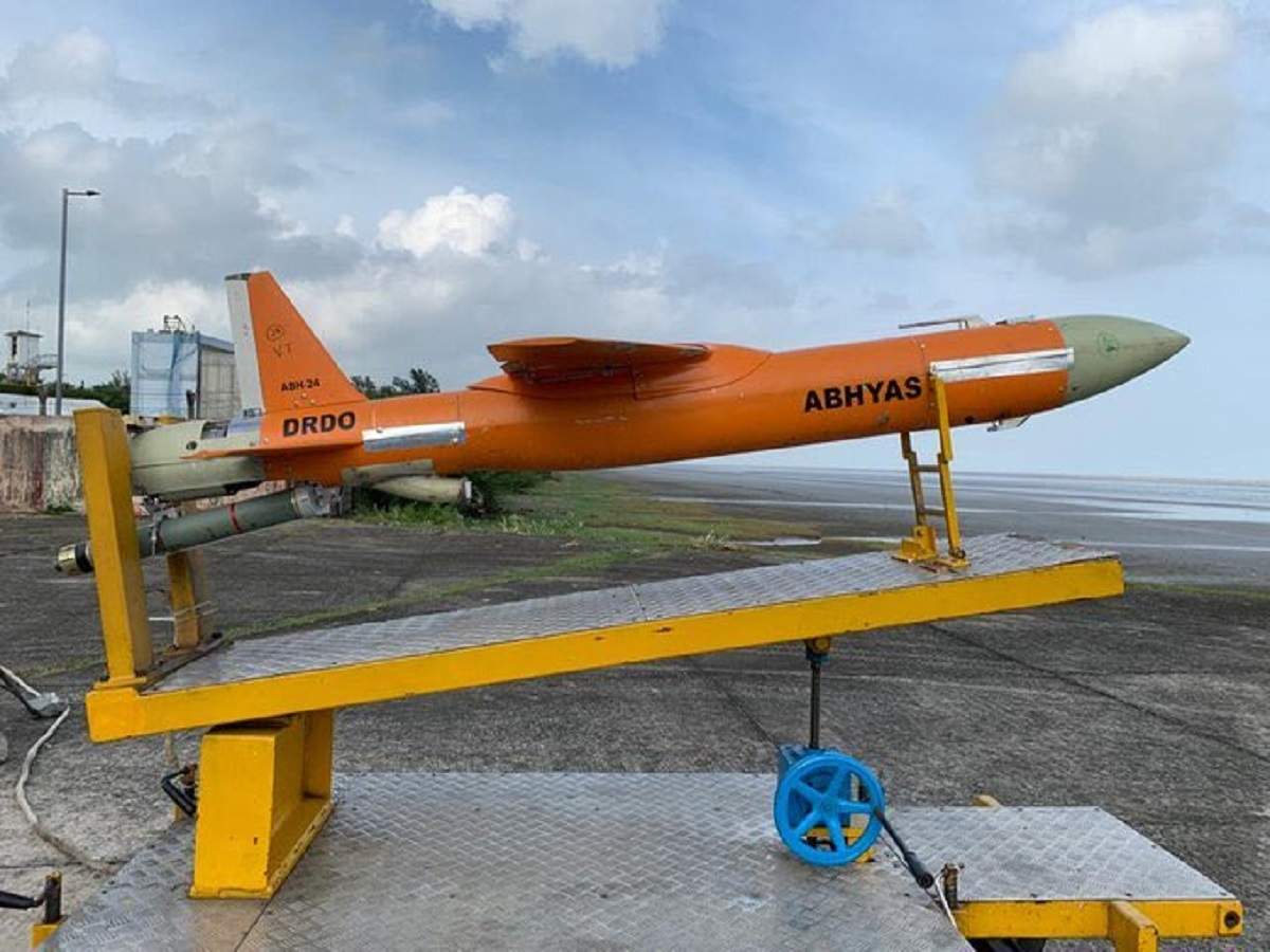
The DRDO Abhyas is an advanced high-speed expendable aerial target (HEAT) developed by the Defence Research and Development Organisation (DRDO) of India. Designed to simulate a variety of aerial threats for weapons testing and training, Abhyas features a radar cross-section (RCS) enhancer, an acoustic miss distance indicator (AMDI), and the ability to replicate different threat profiles. Launched using a twin-booster system, it operates on a gas turbine engine, offering high endurance and maneuverability. Abhyas exemplifies India’s commitment to indigenous defense technology development, supporting robust and realistic training scenarios for the armed forces.
- Type: High-speed expendable aerial target (HEAT)
- Primary Use: Testing surface-to-air and air-to-air missile systems
- Key Features:
- Turbojet engine for extended performance
- Maximum altitude: 5 km
- Applications: Weapon evaluation and air defense training
- Status: Under induction and operational use
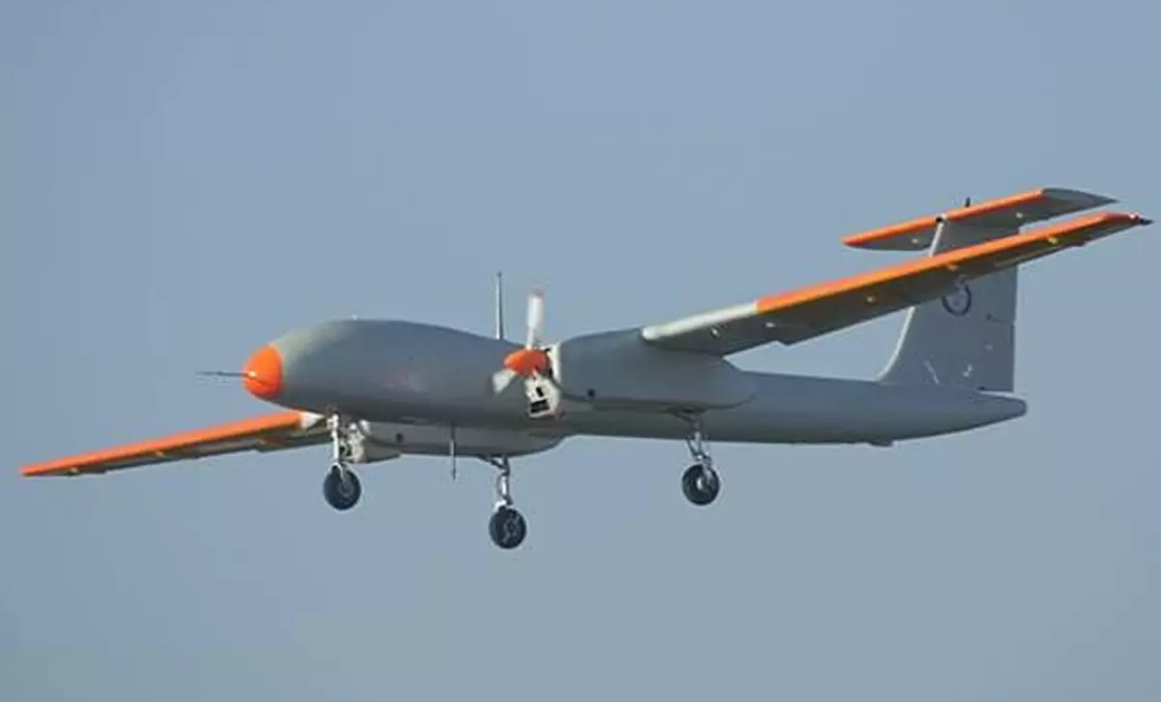
- Panchi
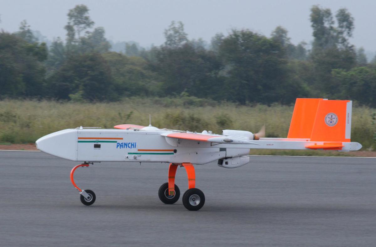
- Type: Wheeled version of the Nishant UAV
- Primary Use: ISR operations with a runway-based takeoff and landing capability
- Key Features:
- Enhanced flexibility compared to Nishant
- Longer endurance due to reduced launch constraints
- Netra (Developed in collaboration with IdeaForge)
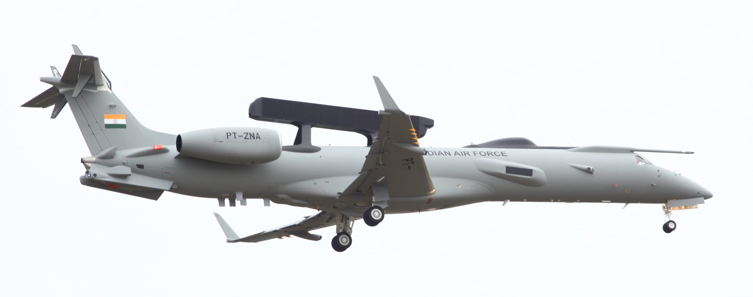
The DRDO Netra is India’s indigenous Airborne Early Warning and Control (AEW&C) system. Mounted on an Embraer EMB-145 platform, Netra features advanced radar and surveillance systems capable of tracking aerial and ground-based targets over a wide range. With a 240-degree coverage and state-of-the-art communication capabilities, it plays a vital role in enhancing situational awareness and supporting tactical operations.
- Type: Mini UAV
- Primary Use: Urban surveillance and crowd monitoring
- Key Features:
- Lightweight quadcopter design
- Real-time video surveillance capability
- Applications: Disaster management, border infiltration monitoring, search and rescue etc.
- Notable Usage: Extensively used during search-and-rescue operations and for monitoring sensitive areas
- Aura (Autonomous Unmanned Research Aircraft)
The AURA program represents India’s ambitious leap into developing an indigenous Unmanned Combat Aerial Vehicle (UCAV). Spearheaded by the Defence Research and Development Organisation (DRDO), AURA is designed for stealth and precision, capable of delivering strategic payloads with minimal detection. Envisioned with advanced composite materials and autonomous systems, it symbolizes a significant advancement in India’s defense technology, aiming to reduce reliance on imports and fortify the nation’s aerial combat capabilities.
- Type: Unmanned Combat Aerial Vehicle (UCAV)
- Primary Use: Stealth operations and precision strikes
- Key Features:
- Design: Flying wing configuration for stealth
- Payload: Precision-guided munitions and ISR equipment
- Status: Development phase with significant potential for high-impact defense missions
- Imperial Eagle
Imperial Eagle is an advanced tactical Unmanned Aerial Vehicle (UAV) developed in collaboration with private industry partners. Designed primarily for surveillance and reconnaissance, the Imperial Eagle is equipped with state-of-the-art sensors and communication systems to support military and paramilitary operations. Its compact design and high endurance make it ideal for monitoring sensitive areas, providing real-time intelligence to enhance operational effectiveness.
- Type: Tactical UAV
- Primary Use: Short-range reconnaissance
- Key Features:
- Lightweight and portable
- Applications: Counter-insurgency and tactical surveillance
- Status: Limited deployment, with potential for scaling
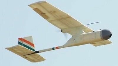
- Pushpak
The NAL/ADE Pushpak is an autonomous Unmanned Aerial Vehicle (UAV) jointly developed by the National Aerospace Laboratories (NAL) and the Aeronautical Development Establishment (ADE), divisions of DRDO. Designed for tactical operations, Pushpak is a lightweight, high-performance UAV primarily intended for surveillance, reconnaissance, and intelligence gathering. With advanced avionics, real-time data transmission capabilities, and robust design, it plays a vital role in enhancing situational awareness across varied terrains, underscoring India’s progress in indigenous UAV technology.
- Type: Fixed-wing UAV
- Primary Use: Environmental monitoring and ISR missions
- Key Features:
- Compact design for ease of deployment
- Applications: Disaster management and environmental surveys
Conclusion
India’s journey into UAV and drone technology, spearheaded by DRDO, reflects a bold vision of self-reliance and innovation in defense. From surveillance-focused UAVs like Nishant to cutting-edge systems like Aura, DRDO’s achievements showcase a blend of ingenuity and strategic foresight. These advancements not only strengthen India’s defense capabilities but also position the nation as a global contender in unmanned aerial systems. As DRDO continues to push the boundaries of technology, it paves the way for a future where Indian innovation becomes a cornerstone of national and global security.
The post Dominating the Skies: DRDO’s UAV Revolution appeared first on ELE Times.
VIPower full bridge with real-time diagnostics reduces complexity and cost of automotive drives
The VNH9030AQ integrated full-bridge DC motor driver handles diverse automotive uses including functional-safety applications. As well as integrating advanced diagnostics, the driver has a dedicated pin for real-time output status that saves external circuitry and slims the bill of materials.
With RDS(on) of 30mΩ per leg, the VNH9030AQ efficiently handles mid- and low-power DC motor driven applications such as door-control modules, washer pumps, powered lift gates, powered trunks, and seat adjusters.
Contributing to the driver’s high overall efficiency, and saving external components, integrated non-dissipative current-sense circuitry monitors the current flowing through the device to distinguish each motor phase. The standby power consumption is very low over the full operating temperature range, easing use in zonal controller platforms.
The VNH9030AQ integrates the high-side and low-side MOSFETs with gate drivers, diagnostics, and protection against overvoltage transients, undervoltage, short-circuit conditions, and cross conduction. Flexibility to configure the MOSFETs either in parallel or in series allows use in systems involving multiple motors or to meet other specific requirements.
The new driver is part of a family of devices that leverage ST’s latest VIPower M09 technology, which permits efficient, monolithic integration of power and logic circuitry. All products feature an innovative 6mm x 6mm thermally enhanced triple-pad QFN package designed for optimal underside cooling and share a common pinout to ease layout and software reuse.
The post VIPower full bridge with real-time diagnostics reduces complexity and cost of automotive drives appeared first on ELE Times.
Swathi Weapon Locating Radar: A Beacon of Indian Defense Technology
India has steadily emerged as a formidable force in defense technology, with indigenous innovations taking center stage. Among its crowning achievements is the Swathi Weapon Locating Radar (WLR), a state-of-the-art radar system designed to detect and track enemy artillery, mortars, and rockets. Developed by Indian defense engineers, the Swathi radar underscores India’s self-reliance in defense capabilities, offering world-class performance at a competitive cost.
What is Swathi Weapon Locating Radar?Swathi Weapon Locating Radar (WLR) is an advanced radar system designed to locate the origin of hostile artillery fire and pinpoint the location of enemy weapons. It provides critical real-time data to armed forces, enabling them to neutralize threats effectively. The radar has been a game-changer for India’s military and has garnered international attention for its capabilities.
Developed by Indian ExpertiseSwathi WLR was developed indigenously by the Electronics and Radar Development Establishment (LRDE), a division of the Defence Research and Development Organisation (DRDO), in collaboration with Bharat Electronics Limited (BEL). This collaboration brought together cutting-edge radar technology and indigenous manufacturing expertise, resulting in a highly reliable and efficient system tailored to the needs of the Indian Armed Forces.
Swathi Radar: Full Form and SignificanceThe term “Swathi” does not have a conventional acronymic full form; it is a name that symbolizes vigilance and precision. In the context of military technology, it signifies the radar’s ability to scan, detect, and act with unparalleled accuracy, much like its namesake.
Swathi’s significance lies in its ability to act as a force multiplier. By detecting and neutralizing threats before they can cause damage, the radar enhances the strategic and tactical advantage of armed forces in conflict scenarios. It also reduces the dependency on foreign-made radar systems, contributing to India’s ‘Make in India’ initiative.
Technical Features and CapabilitiesThe Swathi Weapon Locating Radar boasts several cutting-edge features that make it a world-class system:
- Detection Range: Swathi WLR has a range of up to 50 kilometers for locating artillery and up to 30 kilometers for detecting mortars and rockets. This extended range ensures early threat detection and effective countermeasures.
- Coverage Area: The radar can simultaneously track multiple targets over a wide area, making it ideal for use in complex battlefield scenarios.
- Accuracy: With high precision, the radar can pinpoint the location of enemy weaponry, providing critical data for swift retaliatory action.
- Mobility: Mounted on a mobile platform, the radar can be rapidly deployed in different terrains, from deserts to mountainous regions.
- Weather Resilience: The radar performs reliably under varied weather conditions, ensuring uninterrupted operation during critical missions.
Swathi WLR is not just a domestic asset; it has also made its mark on the international stage. India’s defense exports have grown significantly, with Swathi being a flagship product. Notably, Armenia has procured the radar system, recognizing its exceptional capabilities and cost-effectiveness. This export marked a significant milestone for India’s defense industry, positioning Swathi as a competitive alternative to systems offered by countries like the United States, Israel, and Russia.
The successful export of Swathi underscores the global recognition of India’s indigenous defense technology. It also reflects India’s growing capability to design and manufacture advanced systems that meet international standards.
Cost-Effectiveness: A Strategic Advantage
One of Swathi’s most compelling aspects is its affordability. Priced significantly lower than similar systems from other countries, Swathi offers an attractive option for nations looking to bolster their defense capabilities without overshooting their budgets. The radar’s competitive pricing, combined with its high performance, has made it an appealing choice for several countries exploring modern defense solutions.
Operational Impact and Applications
Swathi WLR has proven invaluable in enhancing battlefield operations. Here’s how:
- Threat Neutralization: By detecting the source of enemy artillery, the radar allows forces to respond quickly and effectively, neutralizing threats before they escalate.
- Border Security: Deployed along sensitive borders, Swathi provides constant surveillance and tracking, ensuring robust national security.
- Counter-Battery Fire: The radar’s ability to accurately locate enemy firing positions enables counter-battery operations, minimizing damage and ensuring tactical superiority.
- International Peacekeeping: Swathi can be deployed in international peacekeeping missions, where its precision and reliability contribute to maintaining stability in conflict zones.
Future Prospects and Upgrades
To maintain its edge, Swathi radar is expected to undergo periodic upgrades, incorporating advancements in radar and sensor technologies. Future iterations may include enhanced range, better integration with command-and-control systems, and AI-driven analytics for real-time decision-making.
Additionally, with an increasing focus on exports, DRDO and BEL are likely to develop customized versions of Swathi to meet the specific needs of different countries.
Conclusion
The Swathi Weapon Locating Radar is a testament to India’s strides in indigenous defense technology. Combining cutting-edge features with cost-effectiveness, it has become a valuable asset for both domestic and international applications. Its successful deployment and export highlight India’s potential to be a global leader in defense innovation. As Swathi continues to evolve, it will undoubtedly remain a cornerstone of India’s defense strategy and a beacon of technological excellence.
The post Swathi Weapon Locating Radar: A Beacon of Indian Defense Technology appeared first on ELE Times.
5G vs LPWA Technologies: A Comparative Overview of 5G, NB-IoT, Sigfox, and LoRa IoT
The Internet of Things (IoT) continues to revolutionize industries by enabling seamless connectivity among devices, sensors, and systems. The choice of communication technology is critical in determining the efficiency, scalability, and cost-effectiveness of IoT implementations. Among the most prominent technologies are 5G and Low Power Wide Area (LPWA) networks, which include NB-IoT, Sigfox, and LoRa. Each of these technologies has distinct characteristics, making them suitable for specific use cases. This article explores the differences between 5G and LPWA technologies, highlighting their unique features, advantages, and limitations.
Understanding the Basics5G Technology
5G is the fifth generation of mobile network technology, designed to provide ultra-fast data speeds, minimal latency, and support for massive device connectivity. It is a versatile technology catering to diverse applications, from enhanced mobile broadband (eMBB) to ultra-reliable low-latency communication (URLLC) and massive machine-type communication (mMTC).
Low Power Wide Area (LPWA) Technologies
LPWA technologies, such as NB-IoT, Sigfox, and LoRa, focus on low power consumption, wide coverage, and cost-efficiency. These technologies are tailored for IoT applications requiring long battery life, low data rates, and devices distributed over vast areas.
Key Features and Capabilities| Feature | 5G | NB-IoT | Sigfox | LoRa |
| Data Speed | Up to 10 Gbps | Up to 250 kbps | 100 bps to 600 bps | 0.3 kbps to 50 kbps |
| Latency | 1 ms or less | ~1.5 seconds | ~10 seconds | ~1 to 5 seconds |
| Coverage | Urban and dense environments | Deep indoor and rural | Global (through operators) | Regional (private networks) |
| Power Efficiency | Moderate | High | Very High | Very High |
| Cost | High | Low to moderate | Low | Low |
Comparing the Technologies
- 5G: High-Speed and Versatility
5G excels in high-bandwidth applications requiring real-time responsiveness. It is ideal for:
- Autonomous Vehicles: Low latency ensures real-time decision-making for self-driving cars.
- Smart Cities: 5G supports dense sensor deployments, enabling smart traffic systems and public safety applications.
- Industrial Automation: Ultra-reliable low-latency communication (URLLC) facilitates advanced robotics and precision manufacturing.
However, 5G’s advanced capabilities come at a higher cost. Its infrastructure demands significant investment, and its power consumption is relatively high, making it less suitable for battery-powered IoT devices.
2. NB-IoT: Simplified Cellular Connectivity
Narrowband IoT (NB-IoT) is a cellular-based LPWA technology developed to address the needs of IoT applications requiring low power consumption and wide coverage. Key applications include:
- Smart Utilities: NB-IoT is widely used in smart metering for water, gas, and electricity.
- Agriculture: It supports soil moisture sensors and livestock monitoring systems.
- Asset Tracking: NB-IoT enables cost-effective tracking of shipping containers and equipment.
NB-IoT operates within the licensed spectrum, ensuring minimal interference and reliable connectivity. Its power efficiency allows devices to run for years on a single battery. However, its data speed and latency are not sufficient for applications requiring real-time responsiveness.
3. Sigfox: Global Connectivity at Low Cost
Sigfox is a proprietary LPWA technology designed for simplicity and affordability. Operating in the unlicensed ISM band, it focuses on:
- Environmental Monitoring: Sigfox supports sensors for air quality, weather, and water levels.
- Smart Logistics: It enables tracking of pallets and packages globally.
- Security Systems: Sigfox connects low-power intrusion sensors and alarms.
Sigfox’s ultra-low data rates and power consumption make it ideal for applications transmitting small amounts of data sporadically. However, its reliance on Sigfox operators limits flexibility and scalability compared to open standards.
4. LoRa: Flexibility and Decentralization
LoRa (Long Range) is an open standard LPWA technology operating in the unlicensed ISM band. It is particularly valued for its:
- Private Networks: LoRa enables businesses to establish their own IoT networks without relying on third-party operators.
- Agriculture and Environmental Use: LoRa supports monitoring of farmlands, forests, and wildlife habitats.
- Smart Buildings: LoRa connects HVAC systems, lighting controls, and security sensors.
LoRa’s flexibility and cost-effectiveness make it a popular choice for localized IoT deployments. However, its reliance on gateways and lack of native global coverage can be limitations for some use cases.
Selecting the Right TechnologyThe choice between 5G and LPWA technologies depends on the specific requirements of the IoT application.
| Consideration | Best Technology |
| High-speed data transfer | 5G |
| Battery life and power efficiency | Sigfox, LoRa, NB-IoT |
| Global connectivity | Sigfox |
| Private network setup | LoRa |
| Real-time responsiveness | 5G |
The Future of IoT Connectivity
As IoT ecosystems continue to expand, hybrid approaches integrating multiple technologies are emerging. For example, 5G can provide high-speed backbone connectivity, while LPWA networks handle localized low-power tasks. Additionally, advancements in edge computing and AI are enhancing the capabilities of all these technologies, enabling more intelligent and efficient IoT solutions.
Conclusion5G and LPWA technologies each bring unique strengths to the IoT landscape. While 5G is the backbone of high-performance, real-time applications, LPWA technologies like NB-IoT, Sigfox, and LoRa cater to cost-sensitive, low-power use cases. The diversity of these technologies ensures that IoT can address a wide spectrum of needs, driving innovation across industries and transforming how we interact with the world around us.
The post 5G vs LPWA Technologies: A Comparative Overview of 5G, NB-IoT, Sigfox, and LoRa IoT appeared first on ELE Times.
Powering a Sustainable Future: A Look at Emerging Sustainable Power Technologies
The world is at a critical juncture. The ever-increasing demand for energy coupled with the looming threat of climate change necessitates a paradigm shift towards sustainable power generation. Thankfully, innovation is blossoming in the realm of renewable energy, with a plethora of emerging technologies poised to revolutionize the way we power our planet.
This article delves into some of the most promising sustainable power technologies that hold immense potential for shaping a cleaner and more secure energy future. We will explore these technologies based on the following categories:
- Solar Energy Advancements
- Wind Power Innovations
- Alternative Renewable Energy Sources
- Energy Storage Solutions
Solar energy remains at the forefront of the renewable energy revolution. However, advancements are constantly pushing the boundaries of efficiency and affordability. Here are some exciting developments:
- Perovskite Solar Cells: These next-generation solar cells boast the potential to surpass the efficiency limits of traditional silicon-based cells. Perovskite materials are lightweight, flexible, and can be manufactured at lower costs, making them ideal for large-scale deployment.
- Concentrated Solar Power (CSP) with Thermal Storage: CSP plants use mirrors to concentrate sunlight onto a receiver, generating heat that can be converted into electricity. Integrating thermal storage allows for continuous power generation even during periods of low sunlight.
- Building-Integrated Photovoltaics (BIPV): BIPV technologies seamlessly integrate solar panels into building materials, transforming rooftops, facades, and windows into power generators. This not only reduces reliance on traditional grids but also enhances building aesthetics.
Wind power is another established renewable energy source, and advancements are focusing on efficiency and harnessing wind energy from untapped sources:
- Offshore Wind Farms: With stronger and more consistent winds blowing offshore, these large-scale wind farms offer significant potential for clean energy generation. Technological advancements in turbine design and floating platforms are making offshore wind farms more cost-effective.
- Vertical Axis Wind Turbines (VAWTs): Unlike traditional horizontal-axis wind turbines, VAWTs can capture wind from any direction, making them suitable for urban environments or areas with unpredictable wind patterns. Their compact design also reduces visual impact.
- High-Altitude Wind Power (HAWP): HAWP systems utilize tethered kites or balloons equipped with turbines to harness the stronger and more consistent winds at high altitudes. This technology is still in its early stages but holds promise for large-scale energy generation.
Beyond solar and wind, a diverse range of renewable energy sources are emerging:
- Geothermal Energy: This technology utilizes the Earth’s internal heat to generate electricity. Enhanced Geothermal Systems (EGS) are expanding the reach of geothermal power by creating artificial geothermal reservoirs in areas with limited natural resources.
- Ocean Energy: The power of waves, tides, and currents can be harnessed through various technologies like wave energy converters, tidal turbines, and ocean thermal energy conversion (OTEC). These technologies are still under development but offer immense potential for coastal regions.
- Biomass Energy: While concerns exist regarding sustainability, advancements in biofuel production and waste-to-energy conversion can contribute to a cleaner energy mix.
The intermittent nature of some renewable energy sources necessitates efficient energy storage solutions. Here are some key technologies:
- Advanced Battery Storage: Lithium-ion batteries are currently the dominant technology, but advancements in solid-state batteries and flow batteries promise higher capacities, longer lifespans, and faster charging times.
- Pumped Hydroelectric Storage (PHES): This mature technology stores energy by pumping water uphill during off-peak hours and releasing it through turbines to generate electricity during peak demand periods.
- Compressed Air Energy Storage (CAES): CAES stores energy by compressing air into underground caverns. When electricity is needed, the compressed air is released to drive turbines and generate power.
The successful integration of these emerging sustainable power technologies requires a collaborative effort. Governments, research institutions, and private companies need to work together to address challenges like:
- Cost Reduction: While advancements are lowering costs, further research and development are crucial to make these technologies cost-competitive with traditional fossil fuels.
- Grid Modernization: Integrating a diverse range of renewable energy sources necessitates a smarter and more flexible grid infrastructure.
- Policy and Regulations: Supportive policies and regulations can incentivize the adoption of renewable energy technologies and create a stable investment environment
The post Powering a Sustainable Future: A Look at Emerging Sustainable Power Technologies appeared first on ELE Times.
Infineon strengthens Sensor and Radio Frequency portfolio with new business unit to drive profitable growth
Infineon Technologies AG, a leader in power, automotive and IoT semiconductors, announced the formation of a new business unit to drive the company’s growth in the area of sensors by combining the existing Sensor and Radio Frequency (RF) businesses into one dedicated organization. The new business unit SURF (Sensor Units & Radio Frequency) will be part of the Power & Sensor Systems (PSS) division and include the former Automotive and Multi-market Sense & Control businesses.
By combining its sensor and RF expertise, Infineon strengthens its competitiveness and go-to-market approach by leveraging cost and R&D synergies accelerating innovation and value to customers. This strategic move will capitalize on the vast market potential of the sensor and RF markets, projected to exceed 20 billion US- Dollars by 2027. The new business unit became effective on 1 January 2025.
“With the new business unit, we are addressing the growing demand for sensors and RF solutions, driven by trends such as green energy, clean and safe mobility, and smart and secure IoT,” says Dr. Thomas Schafbauer, Head of SURF business unit at Infineon. “Our dedicated business unit for sensors and RF allows for the expansion of our sales activities and combines our innovation capabilities, offering even more differentiated system solutions for our automotive, consumer and industrial customers.”
With devices attaining higher levels of intelligence and autonomy, sensor semiconductors are becoming ubiquitous components in connecting the real and digital world: Human Machine Interfaces (HMI) and ambient monitors allow for context-aware devices; Infineon’s microphones based on high-end microelectromechanical systems (MEMS) already play a crucial role in smartphones, wearables, and smart speakers, enabling AI-based language solutions for enhanced consumer experience; Infineon radar solutions enable reliable object recognition e.g. in autonomous driving; And in electric cars and industrial automation, Infineon’s magnetic sensors are key enablers for controlling motion precisely and its current sensors allow for better energy-efficiency in power inverters and batteries.
The post Infineon strengthens Sensor and Radio Frequency portfolio with new business unit to drive profitable growth appeared first on ELE Times.
New Family of Switchtec PCIe Gen 4.0 16-Lane Switches Provides Versatility for Automotive and Embedded Computing Applications
Microchip’s PCI100x devices deliver high performance and cost efficiency for any application where accelerated or specialized computing is used
Efficient management of high-bandwidth data transfer and seamless communication between multiple devices or subsystems are critical in automotive, industrial and data center applications, making PCIe switches an indispensable solution. They provide scalability, reliability and low-latency connectivity, which are crucial for handling the demanding workloads of modern High-Performance Computing (HPC) systems. Microchip Technology today announces sample availability of the new PCI100x family of Switchtec PCIe Gen 4.0 switches in variants to support packet switching and multi-host applications.
The PCI1005 is a packet switch which expands a single host PCIe port to as many as six endpoints. The PCI1003 device enables multi-host connectivity through Non-Transparent Bridging (NTB) and is fully configurable to support from 4–8 ports. All devices are compliant with the PCI-SIG Gen5 specification and operate up to 16GT/s. High-speed DMA is supported on all variants. Advanced Switchtec technology features include Automatic Error Reporting (AER), Downstream Port Containment (DPC) and Completion Timeout Synthesis (CTS). The PCI100x devices are available in wide temperature ranges including commercial (0°C to +70°C), industrial (−40°C to +85°C) and Automotive Grade 2 (−40°C to +105°C) ambient ratings.
“The PCI100x family is a cost-effective solution that does not compromise on high performance and high reliability. It enables designers to now take advantage of PCIe switch capabilities for mass market automotive and embedded computing applications,” said Charles Forni, vice president of Microchip’s USB and networking business unit. “In addition to these connectivity solutions, customers can get many critical components from Microchip including timing, power management and sensors.”
Microchip’s broad portfolio of PCIe switches provides high-density, low-power and reliable solutions for applications like data centers, GPU servers, SSD enclosures and embedded computing. The portfolio also includes Flashtec NVMe controllers and NVRAM drives, Ethernet PHYs and switches, timing solutions and Flash-based FPGAs and SoCs, supporting markets such as storage, automotive, industrial and communications. For more information about PCIe switches.
Pricing and AvailabilityThe PCI1005 and PCI1003 switches are now available in limited sample quantities. Pricing for the PCI1005 commercial variant is $43 each in 1,000-unit quantities (note pricing is subject to change). For additional information and to purchase, contact a Microchip sales representative or visit Microchip’s Purchasing and Client Services website, www.microchipdirect.com.
The post New Family of Switchtec PCIe Gen 4.0 16-Lane Switches Provides Versatility for Automotive and Embedded Computing Applications appeared first on ELE Times.
New MOTIX family of full-bridge ICs for smart brushed DC motor applications enables comfort and convenience in vehicles
With the automotive industry continuing to evolve, features that were once considered premium are now becoming standard. As a result, smart low-voltage motors will play an increasingly important role in shaping tomorrow’s user experience in the vehicle. Automotive manufacturers are looking for more reliable, energy-efficient and cost-effective semiconductor solutions that can work effectively even under the given harsh conditions. To address this demand, Infineon Technologies AG is now expanding its portfolio with the MOTIX Bridge BTM90xx family, a product family of full-bridge/ H-bridge integrated circuits (ICs), specifically designed for brushed DC motor applications. The new BTM90xx full-bridge ICs complement the MOTIX low-voltage motor control IC portfolio spanning from driver ICs to highly integrated system-on-chip (SoC) solutions. BTM90xx devices are not limited to but in particular optimized for automotive applications such as door, mirror, seat, body and zone control modules. Accompanying safety documentation is available to allow use also in safety relevant applications.
The BTM90xx family is characterized by a high functionality to enable intelligent and tiny motor control solutions. The devices, with a supply voltage range for normal operation of 7 V to 18 V (extended 4.5 V to 40 V) offer extensive protection and diagnostic functions such as overtemperature, undervoltage, overcurrent, cross-current or short-circuit detection. Currents are measured for both the high-side and low-side switches and the devices are suitable for automotive applications with a current limit of at least 10 A (BTM901x) or 20 A (BTM902x). PWM operation is possible for frequencies up to 20 kHz. The BTM9011EP and BTM9021EP are SPI variants and support pin-saving daisy chain function to help reduce overall system costs. BTM9021 in addition features an integrated watchdog. The BTM90xx’s tiny TSDSO-14 (4.9 x 6.0 mm) package reduces the overall PCB board space required and features a large exposed pad that simultaneously improves the device’s thermal performance.
To simplify the evaluation and design-in process for MOTIX BTM90xx, Infineon also provides a comprehensive support package, including technical product documentation, simulation models, a tool for calculating power dissipation, evaluation boards and Arduino example code. In addition, software (MOTIX BTM90xx Device Driver) and the MOTIX Full Bridge IC Configuration Wizard are available for free at the Infineon Developer Center (IDC).
The post New MOTIX family of full-bridge ICs for smart brushed DC motor applications enables comfort and convenience in vehicles appeared first on ELE Times.
Navigating the Digital Frontier: Unveiling the Distinction Between Cybersecurity and Ethical Hacking
In the ever-expanding digital landscape, the terms “cybersecurity” and “ethical hacking” often get tossed around interchangeably. While both disciplines share a common goal – protecting our valuable data and systems from malicious actors – their approaches and objectives diverge significantly. Understanding these distinctions is crucial for navigating the complex terrain of the digital frontier.
Cybersecurity: Building the FortressCybersecurity can be likened to a meticulously constructed fortress, safeguarding our digital assets from unauthorized access, theft, disruption, modification, or destruction. It encompasses a comprehensive set of strategies, technologies, and practices designed to deter, detect, and mitigate cyberattacks.
- Defense in Depth: Cybersecurity professionals employ a layered defense approach, akin to building multiple walls around a castle. This includes firewalls, intrusion detection/prevention systems (IDS/IPS), data encryption, access controls, and user education. Each layer serves as a barrier, making it progressively harder for attackers to breach the system.
- Continuous Monitoring: Vigilance is paramount in cybersecurity. Security professionals constantly monitor network activity, system logs, and user behavior for anomalies that might indicate a potential attack. Security Information and Event Management (SIEM) systems play a vital role in this ongoing process, aggregating data from various sources and providing real-time insights into potential threats.
- Incident Response: Despite the best-laid plans, cyberattacks can still occur. Cybersecurity professionals develop and implement incident response plans to effectively respond to security breaches. These plans outline procedures for containing the damage, eradicating the threat, and restoring affected systems.
Ethical hacking, on the other hand, embodies a proactive approach to cybersecurity. Ethical hackers, also known as white hat hackers or penetration testers, are security professionals who are authorized to simulate cyberattacks on a system or network. Their objective is to identify vulnerabilities that malicious actors might exploit and recommend appropriate security measures to address them.
- Vulnerability Assessment and Penetration Testing (VAPT): This is the cornerstone of ethical hacking. Ethical hackers employ a variety of tools and techniques, mirroring those used by real-world attackers, to probe for weaknesses in systems and networks. They may attempt to gain unauthorized access, exploit software vulnerabilities, or bypass security controls.
- Social Engineering Assessments: Ethical hackers don’t just focus on technical vulnerabilities. They also assess the human element of security by conducting social engineering simulations. This involves mimicking tactics used by attackers, such as phishing emails or pretext calls, to evaluate employee awareness and susceptibility to social engineering attacks.
- Red Teaming and Purple Teaming: Ethical hacking can be taken a step further through red teaming and purple teaming exercises. Red teaming exercises simulate a full-blown cyberattack, allowing organizations to assess their overall security posture and response capabilities. Purple teaming exercises involve collaboration between ethical hackers and security teams, fostering communication and knowledge sharing to strengthen the organization’s defenses.
While cybersecurity and ethical hacking operate on different sides of the digital security spectrum, they share a symbiotic relationship. Cybersecurity professionals rely on the insights gleaned from ethical hacking to identify and address vulnerabilities before they can be exploited by malicious actors. Ethical hackers, in turn, depend on a strong understanding of cybersecurity principles and best practices to effectively simulate real-world attacks.
Key Distinctions: A Comparative Analysis- Objectives: Cybersecurity aims to defend systems and data from unauthorized access and attacks. Ethical hacking, on the other hand, proactively identifies vulnerabilities in systems to improve security posture.
- Methodology: Cybersecurity professionals employ a defensive approach, deploying security tools and monitoring systems for suspicious activity. Ethical hackers take an offensive stance, simulating attacks to uncover vulnerabilities.
- Legality: Cybersecurity activities are always legal and authorized. Ethical hacking is legal only when conducted with explicit permission from the system or network owner.
- Outcomes: Effective cybersecurity practices minimize the risk of cyberattacks. Ethical hacking identifies vulnerabilities that can be addressed to strengthen overall security.
The recognition of the value of ethical hacking has led to the emergence of bug bounty programs. These programs incentivize security researchers to identify and report vulnerabilities in software or systems. Organizations can leverage these programs to discover and address vulnerabilities before they are exploited by malicious actors.
Conclusion: A United Front in the Digital AgeCybersecurity and ethical hacking, though distinct disciplines, are both essential components of a comprehensive digital security strategy. By combining the proactive vulnerability identification of ethical hacking with the defensive measures of cybersecurity, organizations can create a robust and innovative security ecosystem that can adapt to the rapidly changing threat landscape and safeguard our increasingly interconnected digital world.
The post Navigating the Digital Frontier: Unveiling the Distinction Between Cybersecurity and Ethical Hacking appeared first on ELE Times.
The Interwoven Tapestry of the Internet of Things Weaving a Smarter Future
The Internet of Things (IoT), a revolutionary concept seamlessly intertwining the physical and digital realms, is no longer a distant futuristic vision but a rapidly unfolding reality. At its core, IoT represents a vast network of interconnected devices—ranging from the mundane to the extraordinary—imbued with the ability to sense, communicate, and act upon their environment. From wearable fitness trackers and household appliances to industrial machinery and precision agricultural tools, IoT’s potential to transform our world is profound and unprecedented.
The Foundation of Connectivity: Data as the LifebloodThe genesis of IoT lies in its capacity to generate, collect, and utilize data. Embedded within these interconnected devices are arrays of sensors—meticulously designed instruments that monitor a myriad of parameters such as temperature, humidity, motion, location, and more. These sensors act as the IoT’s nervous system, continuously gathering data from their environment. Once collected, this raw data becomes the lifeblood of IoT, driving transformative applications across various industries.
However, the process doesn’t end with data collection. IoT’s effectiveness depends heavily on its ability to transmit this data reliably and efficiently. The advent of high-speed networks, particularly 5G technology, has proven instrumental in this endeavor. With its ultra-low latency, high data transfer speeds, and capacity to connect billions of devices simultaneously, 5G serves as the critical backbone for real-time data exchange. This capability is crucial for applications like autonomous vehicles, which rely on instantaneous communication with traffic signals and other vehicles, or remote surgical procedures that demand precise, latency-free control.
The Intelligence Quotient: AI and Machine LearningWhile the collection and transmission of data form the foundational layers of IoT, the true transformative power lies in intelligent data processing and interpretation. Artificial Intelligence (AI) and Machine Learning (ML) algorithms are pivotal in this aspect, acting as the cognitive engines of IoT.
AI systems analyze massive datasets to uncover intricate patterns and predict future outcomes. For instance, in manufacturing, AI-powered predictive analytics can monitor sensor data from industrial equipment to forecast potential failures, enabling proactive maintenance and minimizing costly downtime. Similarly, in smart cities, AI algorithms analyze traffic flow and identify congestion hotspots, optimizing traffic management systems to reduce delays and improve urban mobility.
Machine Learning models also enhance IoT by enabling devices to adapt to changing conditions over time. Smart thermostats, for example, learn user preferences and environmental patterns to optimize energy consumption without manual intervention.
A Tapestry of Applications: Weaving a Smarter WorldIoT’s impact extends across multiple industries, each leveraging its potential to innovate and optimize operations.
- Smart Cities
IoT technologies are integral to building smart cities, where interconnected systems manage resources efficiently and sustainably. Smart grids optimize energy distribution, intelligent traffic systems reduce congestion, and IoT-enabled sensors monitor air quality to improve urban health standards. Cities like Singapore and Barcelona have already implemented IoT solutions to enhance public safety, transportation, and energy efficiency.
- Healthcare
In healthcare, IoT has revolutionized patient care through wearable devices and remote monitoring systems. These devices collect real-time health data, such as heart rate, blood pressure, and glucose levels, enabling personalized and proactive medical interventions. Remote monitoring also allows healthcare providers to track patients’ conditions outside hospital settings, reducing costs and improving accessibility.
- Industrial Automation
The Industrial Internet of Things (IIoT) is driving significant advancements in manufacturing and supply chain management. Smart factories utilize interconnected machines to monitor production processes, detect anomalies, and optimize workflows. Predictive maintenance powered by IoT sensors reduces equipment downtime, while real-time tracking enhances inventory management and logistics.
- Agriculture
Precision agriculture leverages IoT-enabled sensors to monitor soil moisture, weather conditions, and crop health. Farmers can optimize irrigation schedules, apply fertilizers more effectively, and predict pest infestations, leading to higher yields and reduced environmental impact. These technologies are especially valuable in addressing the challenges of food security and climate change.
- Consumer Electronics
Smart home devices, such as voice-activated assistants, connected lighting systems, and intelligent appliances, have become mainstream. These devices enhance convenience and energy efficiency, creating personalized living environments for users.
The Future of IoT: A Horizon of PossibilitiesThe evolution of IoT is an ongoing journey fueled by technological innovation. Several key trends are shaping its future:
- Edge Computing
As the volume of data generated by IoT devices continues to explode, the need for decentralized processing becomes critical. Edge computing addresses this challenge by processing data closer to its source, reducing latency and bandwidth requirements. Applications such as autonomous vehicles and industrial automation greatly benefit from the responsiveness enabled by edge computing.
- Blockchain Technology
Blockchain’s inherent security and transparency make it a valuable tool for IoT. By providing tamper-proof data storage and secure transaction mechanisms, blockchain enhances trust within the IoT ecosystem. This is particularly important for applications involving sensitive data, such as healthcare and finance.
- Low-Power Wide-Area Networks (LPWAN)
Technologies like LoRaWAN and NB-IoT are expanding the reach of IoT into remote and challenging environments. These networks enable long-range communication for battery-powered devices, supporting applications in agriculture, logistics, and environmental monitoring.
- Interoperability and Standards
The diverse array of devices and platforms in the IoT ecosystem necessitates standardized communication protocols. Efforts to establish universal standards will be critical for ensuring seamless integration and scalability across different IoT applications.
- Sustainability
As IoT adoption grows, so does its environmental impact. The development of energy-efficient devices, sustainable manufacturing practices, and recycling programs for IoT components will be essential to mitigate this impact.
Challenges and ConsiderationsDespite its potential, IoT faces several challenges that must be addressed:
- Security and Privacy: With billions of connected devices, the risk of cyber-attacks and data breaches is significant. Implementing robust security measures, such as encryption and real-time threat detection, is crucial.
- Scalability: Managing the massive influx of IoT devices and data requires scalable infrastructure and efficient resource allocation.
- Cost and Accessibility: The initial investment in IoT infrastructure can be prohibitive for smaller organizations, underscoring the need for cost-effective solutions.
- Regulatory Compliance: As IoT applications intersect with various industries, ensuring compliance with regulatory standards is a complex yet essential task.
The Internet of Things represents a paradigm shift, a convergence of technology, data, and intelligence poised to reshape our world. By harnessing the power of interconnected devices, AI-driven insights, and robust communication networks, IoT has the potential to create a smarter, more sustainable future. From optimizing urban living to revolutionizing healthcare and agriculture, the applications of IoT are as diverse as they are impactful.
As we continue to navigate this transformative era, addressing challenges such as security, interoperability, and sustainability will be paramount. With continued innovation and collaboration, IoT stands ready to enrich the human experience, weaving a tapestry of connectivity and intelligence that defines the future.
The post The Interwoven Tapestry of the Internet of Things Weaving a Smarter Future appeared first on ELE Times.
STMicroelectronics recognized as a Global Top Employer 2025
- STMicroelectronics has been awarded “Top Employer Global” certification for the first time
- 17 companies in the world have obtained this international certification for 2025
- ST entities in 41 countries certified as Top Employer
STMicroelectronics, a global semiconductor leader serving customers across the spectrum of electronics applications, has been recognized for the first time as a global Top Employer for 2025 by Top Employers Institute.
This year STMicroelectronics was one of only 17 global Top Employers to be recognized by Top Employers Institute for their outstanding HR policies and practices worldwide, covering ST entities in 41 countries. The Top Employers Institute program certifies organizations based on the participation and results of their HR Best Practices Survey. STMicroelectronics was distinguished in this ranking thanks to a continuous improvement approach and stands out particularly in the themes of Ethics & Integrity, Purpose & Values, Organization & Change, Business Strategy, and Performance.
“A couple of years ago, we began a people-centric transformation to enhance our leadership culture, simplify and digitalize people processes, with the employee journey and experience as our north star. Achieving the Top Employer Global certification confirms that our efforts are well-directed, and that ST is a place where every talent can thrive, regardless of their career stage or perspective,” said Rajita D’Souza, President, Human Resources & Corporate Social Responsibility, STMicroelectronics.
“We’re excited that STMicroelectronics certified as a global Top Employer for the first time. They have particularly showcased their strengths in areas such as Organisation & Change, Ethics & Integrity, Purpose & Values and Business Strategy. This Certification shows ST’s commitment to creating a better world of work through their HR initiatives and practices, by demonstrating how they support their colleagues across 41 countries,” said David Plink, CEO Top Employers Institute.
The Top Employers Institute survey, followed by validation and audit, covers six HR domains consisting of 20 topics including People Strategy, Work Environment, Talent Acquisition, Learning, Diversity & Inclusion, Wellbeing and more. The program has certified and recognized over 2,400 Top Employers in 125 countries/regions across five continents.
The post STMicroelectronics recognized as a Global Top Employer 2025 appeared first on ELE Times.
Pages

