
ELE Times

TOYOTA Selects Infineon’s SiC Power Semiconductors for its New, “bZ4X”
Infineon Technologies announced that CoolSiC MOSFETs (silicon carbide (SiC) power MOSFETs) have been adopted in the new bZ4X model from Toyota, the world’s largest automaker. Integrated into the on-board charger (OBC) and DC/DC converter, the SiC MOSFETs leverage the material’s advantages of low losses, high thermal resistance, and high voltage capability to help extend driving range and reduce charging time.
“We are very proud that Toyota, one of the world’s largest automakers, has chosen Infineon’s CoolSiC technology. Silicon carbide enhances the range, efficiency and performance of electric vehicles and is therefore a very important part of the future of mobility,” said Peter Schaefer, Executive Vice President and Chief Sales Officer Automotive at Infineon. “With our dedication and our commitment to innovation and zero-defect quality, we are well-positioned to meet the growing demand for power electronics in electromobility.”
Infineon’s CoolSiC MOSFETs feature a unique trench gate structure that reduces normalised on-resistance and chip size, enabling reductions in both conduction and switching losses to contribute to higher efficiency in automotive power systems. In addition, optimised parasitic capacitance and gate threshold voltage enable unipolar gate drive, contributing to the simplification of drive circuits for automotive electric drive train and supporting high-density, high-reliability design for OBC and DC/DC converters.
The post TOYOTA Selects Infineon’s SiC Power Semiconductors for its New, “bZ4X” appeared first on ELE Times.
STMicroelectronics expands strategic engagement with AWS, enabling high-performance compute infrastructure for cloud and AI data
STMicroelectronics has announced an expanded strategic collaboration with Amazon Web Services (AWS) through a multi-year, multi-billion USD commercial engagement serving several product categories. The collaboration establishes ST as a strategic supplier of advanced semiconductor technologies and products that AWS integrates into its compute infrastructure, enabling AWS to provide customers with new high-performance compute instances, reduced operational costs, and the ability to scale compute-intensive workloads more effectively.
As part of this expanded relationship, ST will work with AWS to optimise electronic design automation (EDA) workloads in the cloud. AWS’s scalable compute power enables silicon design acceleration, parallelises design tasks, and gives engineering teams the flexibility to handle dynamic compute demands and speed products to market.
Commercial Agreement
This engagement covers a broad range of semiconductor solutions leveraging ST’s portfolio of proprietary technologies. ST will supply specialised capabilities across high-bandwidth connectivity, including high-performance mixed-signal processing, advanced microcontrollers for intelligent infrastructure management, as well as analogue and power ICs that deliver the energy efficiency required for hyperscale data centre operations.
The collaboration will help customers reduce the total cost of ownership and bring products to market faster. ST’s specialised technologies help AWS address the increasing demands for compute performance, efficiency, and data throughput required to support growing AI and cloud workloads.
Jean-Marc Chery, ST President & CEO, commented: “This strategic engagement establishes ST as an important supplier to AWS and validates the strength of our innovation, proprietary technology portfolio, and proven manufacturing-at-scale capabilities. Our advanced semiconductor solutions will directly power AWS’s next-generation infrastructure, enabling its customers to push the boundaries of AI, high-performance computing, and digital connectivity. This collaboration positions us ideally for further scale-up across multiple market segments, from data centre infrastructure to AI connectivity, positioning ST at the centre of the AI revolution.”
ST has issued warrants to AWS for the acquisition of up to 24.8 million ordinary shares of ST. The warrants will vest in tranches over the term of the agreement, with vesting substantially tied to payments for ST products and services purchased by AWS and its affiliates. AWS may exercise the warrants in one or more transactions over a seven-year period from the issue date at an initial exercise price of $28.38.
The post STMicroelectronics expands strategic engagement with AWS, enabling high-performance compute infrastructure for cloud and AI data appeared first on ELE Times.
GaN Benefits in Motor Controls
By: Ester Spitale, Technical Marketing Manager, STMicroelectronics and Albert Boscarato, Application Lab Manager, STMicroelectronics

GaN benefits in different applications
The major challenge of power electronics today is dealing with the growing need for improved efficiency and power performance, and at the same time, the constant pursuit of cost and size reductions.
The introduction of Gallium Nitride (GaN) technology, a relatively new wide bandgap compound, moves in this direction, as it becomes increasingly available commercially, its use is growing tremendously.
With a better figure-of-merit (FOM), on-resistance RDS(on), and total gate charge (QG) than silicon counterparts, High-electron-mobility transistor (HEMT) devices based on gallium nitride (GaN) also offer a high drain to source voltage capability, zero reverse recovery charge and very low intrinsic capacitances.
The first application where GaN technology has spread is power conversion: GaN represents the leading solution for improving efficiency, making it possible to meet the most stringent energy requirements. The capability to work at higher switching frequencies enables higher power densities, and therefore reduction of the system dimensions, weight and cost.
Size and energy efficiency are also crucial in electronic motor designs: minimising conduction and switching losses in the drive is key for reducing energy waste.
Performance improvement in motor drivers relying on classic silicon MOSFETs and IGBTs is becoming more difficult as silicon technology approaches theoretical limits for power density, breakdown voltage, and switching frequency. Due to their superior electrical characteristics, GaN transistors are a valid alternative to MOSFETs and IGBTs in high-voltage motor control applications.
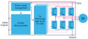 Simplified block diagram of a power inverter based on GaN transistors
Fueling the next generation of motor inverters
GaN is promising important benefits even in applications operating at low frequencies (up to 20kHz). In the realm of home appliances, motor-driven systems such as washing machines, refrigerators, air conditioners, and vacuum cleaners rely heavily on motor inverters to control speed, torque, and efficiency. Unlike industrial servo or precision motors, the physical size of these motors is largely fixed due to mechanical and functional constraints. This means that the traditional approach of reducing overall system size by shrinking the motor itself is not feasible. Instead, improvements must be sought in the inverter and power electronics that drive these motors.
In this sense, it is important to point out that the benefit of GaN over traditional silicon transistors does not come from a single parameter that stands out. It is rather the sum of different aspects concatenating together.
GaN has a de facto negligible reverse recovery charge (Qrr) and low parasitic capacitances, which in turn enable working with slightly higher dV/dt. While the motor winding and insulation limit the maximum allowable dV/dt, GaN’s capability to operate at higher switching speeds allows designers to optimise switching edges carefully.
Moreover, a safe and drastic reduction of dead-time is also achievable without risking shoot-through faults. Time between high-side and low-side switching can be easily lowered by a factor of 10. This can improve inverter efficiency and reduce switching losses without compromising motor reliability.
As remarkable as it gets, the performance is not over yet. In fact, all these “little” improvements combined lead to what may be considered the most relevant of them all: the removal of the heatsink.
Kiss your heatsink goodbye
The considerable reduction in power dissipation allows designers to reduce or even remove bulky heatsinks in the inverter power stage. The assembly line may now require fewer steps in the manufacturing process. No heatsink also means no screws or mounting joints, thus avoiding mechanical failures that can appear when the appliance is already long in the field. An interesting potential saving of service and warranty costs.
The overall result is a more compact, lightweight, and cost-effective inverter design that fits better within the demanding and highly competitive space of the home appliances market.
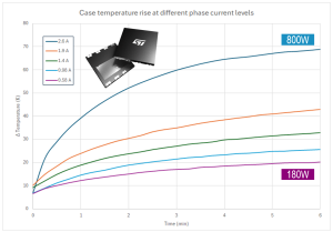 700 V GaN mounted on a motor inverter running without a heatsink
The waveforms show how smooth and cold a GaN can be. In the example above, the device under test has a typical RDS(on) of 80mΩ. The motor inverter runs at a switching frequency of 16 kHz, with a maximum dV/dt slightly under 10V/ns.
A power level of about 800 W can be safely achieved without incurring thermal runaway. The increase in temperature Δt is less than 70 °C, which leaves a good margin before reaching the maximum operating junction temperature (TJmax) of 150 °C.
This remarkable result is achieved without a heatsink, with GaNs mounted on and cooled down through a common 2-layer PCB.
STPOWER GaN Transistors
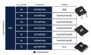
STPOWER GaN Transistors are intrinsically normally off, p-GaN gate e-mode transistors that offer a zero reverse recovery charge. ST offers today seven part numbers rated 700 V breakdown voltage (VDS), with typical on-resistance RDS(on) ranging from 270 mΩ down to 53 mΩ in DPAK, PowerFLAT 8×8, and TO-LL packages.
The portfolio is rapidly growing, adding on different packages, RDS(on) and breakdown voltage levels.
The post GaN Benefits in Motor Controls appeared first on ELE Times.
Union Minister Ashwini Vaishnaw inaugurates TI’s new, world-class R&D centre
Texas Instruments (TI) officially opened its new, state-of-the-art product research and development (R&D) centre in Bengaluru at an event commemorating the company’s 40-year presence in India. As the first multinational company to establish an R&D centre in India in 1985, TI has been instrumental in shaping India’s semiconductor landscape for four decades. The new 550,000-square-foot centre features a collaborative workspace dedicated to developing world-class chip designs. The centre includes an end-to-end reliability lab equipped with advanced testing capabilities for various environmental conditions, along with many other integrated circuit design labs.
Inaugurated by Shri Ashwini Vaishnaw, Union Minister for Railways, Information & Broadcasting, Electronics & Information Technology, Government of India, alongside TI leaders, the new centre highlights the company’s strategic vision to propel semiconductor innovation and nurture world-class design talent. This expansion reinforces TI’s commitment to developing breakthrough analogue and embedded processing technologies while strengthening its support for the design ecosystem and its growing customer base in India.
Shri Ashwini Vaishnaw, Union Minister for Railways, Information & Broadcasting; Electronics & Information Technology, Government of India, said, “I congratulate Texas Instruments on the inauguration of this world-class R&D centre in Bengaluru. TI has been a true pioneer in India’s semiconductor journey and stood as a testament to consistently nurturing the design talent ecosystem in India. The company’s expanded investment reinforces India’s position as a global hub for semiconductor design, development and supports our vision of building an innovation-led nation.”
Santhosh Kumar, president and managing director, TI India, said, “As we celebrate 40 years in India, this milestone reflects TI’s rich legacy and our strong commitment to the future. TI India’s product development and design teams drive research and breakthrough innovations for customers worldwide. Our world-class engineers are central to pioneering the next generation of semiconductor advancements.”
The company recently opened an additional sales office to strengthen its partnership with Indian customers, while the new R&D facility builds on its innovation capabilities in the region. With thousands of employees in India, TI continues to expand its presence in the region.
The post Union Minister Ashwini Vaishnaw inaugurates TI’s new, world-class R&D centre appeared first on ELE Times.
Bridging the design-to-deployment gap: How India can lead the next wave of connected device innovation
Hareesh Ramana, Chief Experience Officer, Sasken Group & President, Borqs Technologies (a Sasken Group company)
India is making significant strides in electronics manufacturing with the aim of 38% value addition within five years. The device manufacturing ecosystem has grown to a significant scale, but it still depends heavily on designs and reference architectures developed elsewhere.
Building domestic capability in electronic device design, especially IoT/connected device design, is critical to India’s ambition of becoming a major electronics manufacturing hub. India’s ambition to reach 38% value addition in electronics manufacturing will be driven not only by scaling assembly but by strengthening device design and systems engineering, which can contribute as much as 30-35% of the total value creation.
Need for in-house design capabilities:
A growing model in India’s connected-device ecosystem is design-led, end-to-end IoT product development anchored locally, covering silicon integration, embedded software, connectivity stacks, and certification. Companies like Borqs Technologies (now part of the Sasken Group) exemplify this approach, offering full-stack IoT design capabilities from within India. For OEMs, this can shorten development cycles, improve control over system integration, and reduce dependence on externally sourced IP and engineering capacity, especially in critical connectivity and compliance stages. Expanding these capabilities across the industry can help India move beyond contract manufacturing and toward the higher-value innovation layer where devices connect to data, analytics, and services.
Time to market gap:
Many IoT projects stall because hardware, firmware, cloud platforms, connectivity, and certification are handled by separate vendors with misaligned priorities.
Over the past decade, India’s product development ecosystem has matured to address these challenges, evolving from a cost-centric outsourcing base into a design-led innovation hub. Global OEMs and platform companies increasingly view India as a partner for rapid prototyping and co-innovation, not just low-cost assembly. Several end-to-end product engineering companies in India exemplify this shift by delivering integrated IoT solutions that shorten development cycles and align with global OEM roadmaps.
Integration as a strategic capability
Connected devices are no longer standalone products; they are endpoints of digital services. The differentiator is therefore systems integration across silicon, hardware, software, connectivity, and lifecycle management. A unified, end-to-end engineering model can enable:
- Faster debugging by tightening the feedback loop between hardware and software teams
- Fewer integration issues by reducing handoffs across multiple vendors
- Quicker prototyping and validation through coordinated design and test cycles
- More predictable certification and production ramp by planning compliance and manufacturability early
- A single accountable partner from concept through delivery and lifecycle management
This is particularly vital for industrial-grade devices where reliability, security, and compliance define adoption. Indian engineering firms with cross-layer capabilities are increasingly enabling platform-driven approaches that allow module reuse across verticals like automotive, energy management, and logistics.
AI and advanced technologies and product development:
Advanced technologies like AI, IoT, automation, digital twins, and cloud computing are transforming product development. AI-driven analytics reduce manual testing cycles, while digital twins simulate device behaviour under real-world conditions, enabling faster iteration and higher reliability.
Demand for software-defined vehicles, smart energy infrastructure, automated factories, and connected appliances is accelerating globally. Multinationals are expanding design centres and co-innovation programs in India to build products for both developed and emerging markets.
For India, the opportunity lies in moving beyond contract manufacturing to the high-value layer where devices meet data, analytics, and services. Mastery over sensors, edge intelligence, connectivity stacks, and lifecycle platforms can enable the country to capture a far greater share of the global electronics economy.
The coming decade will reward ecosystems that can bridge the design-to-deployment gap with reliability and speed. India has the talent, digital infrastructure, and entrepreneurial energy to lead this shift. The next step is an integrated approach that unites design, engineering, and manufacturing into a single innovation continuum.
The post Bridging the design-to-deployment gap: How India can lead the next wave of connected device innovation appeared first on ELE Times.
ST Foundation Continues Expansion of Digital Literacy Initiatives in India; Honours IFCCI ‘CSR Project of the Year’ Recognition
The ST Foundation, the non-profit corporate arm of STMicroelectronics, hosted a media briefing late January 2026 to outline its strategic expansion in India and celebrate the recent recognition of its flagship “Digital Unify” program. Dedicated to bridging the global digital divide since 2001. The Foundation’s mission has taken on critical urgency in India, where over 400 million people remain excluded from essential digital services.
Addressing the 400 Million Divide
With global data from the 2025 ITU Connectivity Report indicating that 2.2 billion people lack basic digital access, the ST Foundation has positioned India as a central focus for its “Digital Unify” (DU) initiative. The program uses a “train-the-trainer” model and local partnerships to ensure sustainable, community-owned growth.
Impact in Asia and India
In Asia alone, the foundation has 96 Digital Unify Labs, serving about 26,000 beneficiaries per year at a cost of less than $10 per student trained.
The Foundation in India was officially registered in 2018, having reached more than 180,000 trainees to date and having established over 56 Digital Unify Labs across the country.
Key Program Impact and Expansions:
- Education for Vulnerable Children: Since 2022, the “Basic Coding” program has reached over 2,500 children aged 9–13 in slum areas, providing many with their first-ever exposure to digital devices.
- Rehabilitation for Incarcerated Individuals: In partnership with the India Vision Foundation, the “Introduction to Computer Basics” (ICB) course has trained over 3,300 incarcerated people across Uttar Pradesh and Delhi (including Central Jail Rohini) to aid in their eventual reintegration into society.
- Empowering the Visually Impaired: A specialised ICB4VI pilot recently trained 17 visually impaired girls in digital skills. The Foundation is now preparing to scale this model nationwide.
Digital Unification and Cyber Concerns
The Foundation has not only been providing underprivileged people with digital literacy but has also helped them with understanding the basic risks of cyber-attacks, briefings on cybersecurity and internet safety.
Award-Winning Impact
The briefing also highlighted the Foundation’s recent accolade as the “CSR Project of the Year” at the 7th Indo-French Chamber of Commerce & Industry (IFCCI) CSR Conclave & Awards. This award recognises the program’s effectiveness in turning the digital access gap into tangible opportunities for education and employment.
By: Shreya Bansal, Sub-Editor
The post ST Foundation Continues Expansion of Digital Literacy Initiatives in India; Honours IFCCI ‘CSR Project of the Year’ Recognition appeared first on ELE Times.
R&S drives connections and innovations at MWC Barcelona 2026
Rohde & Schwarz will exhibit its extensive portfolio of next generation of wireless technologies, under the motto, “Enabling Connections, Empowering Innovations”, at the Mobile World Congress 2026 in Barcelona, Fira Gran Via, hall 5, booth 5A80 from March 2 to 5, 2026.
The path from 5G to 6G
For a seamless evolution from 5G to 6G, Rohde & Schwarz offers future-ready test solutions for mobile devices and networks. Among the many innovative solutions, the CMX500 one-box signalling tester stands out throughout multiple demos, addressing today’s and tomorrow’s testing challenges.
- Paving the way for 6G, Rohde & Schwarz showcases carrier aggregation combining FR1 and FR3 frequency ranges with its CMX500 one-box signalling tester. The demonstration validates end-to-end device behaviour across the aggregated spectrum. FR3 (7.125 to 24.25 GHz) has been identified by industry and research as a “sweet spot” for combining wide-area coverage with high capacity. Equipped with the new, upgradeable RFU18 board for the CMX500, the tester covers up to 18 GHz, giving users enough headroom for FR3 evolution and a future-ready path for testing next-generation networks.
- Another setup addresses virtual signalling testing. Based on the CMX500, Rohde & Schwarz demonstrates a new approach of shift-left testing, allowing R&D engineers to find design flaws early in their mobile radio modem chips before costly silicon fabrication. This early SDR-based validation will significantly cut time-to-market for 6G devices.
- Ray tracing simulates real-world signal propagation environments, making it a valuable technique for AI receiver testing for future 6G devices. Rohde & Schwarz will showcase the CMX500 as it creates a digital twin of signal propagation within its test environment by leveraging the VIAVI
 ray tracing engine. This enables controlled and reproducible validation of complex scenarios with high measurement precision, facilitating site-specific optimisation of radio links and reducing the need for tedious field tests.
 - Rohde & Schwarz also advances 5G and emerging 6G testing with its AI-based toolset AI Workplace for the CMX500, massively enhancing testing productivity. TechAssist uses natural language to control the CMX500, enabling rapid test-scenario setup and status/configuration queries, while an upgraded ScriptAssist with a new interface simplifies and accelerates scripting for R&D protocol and application testing as well as instrument automation. Visitors can experience these AI-powered tools in action within various setups at MWC 2026.
- Mobile XR and personal AI devices like smart glasses and wearables are key for 5G-Advanced and 6G-enabled immersive 3D communications. Delivering compelling, low-latency experiences will require rigorous, realistic testing. Rohde & Schwarz will demonstrate an end-to-end testbed centred around the CMX500, addressing AI on RAN and XR testing challenges with its ability to emulate 4G, 5G and Wi-Fi networks, applying both RF and IP impairments to reproduce real-world conditions such as interference and congestion.
- 6G ISAC (Integrated Sensing and Communication), which leverages mobile networks for object detection, is rapidly gaining traction. Rohde & Schwarz will demonstrate new capabilities of its R&S AREG800A, including the emulation of micro-Doppler signatures – in addition to distance, speed and RCS – to support object classification, such as drones.
- For testing base stations and network infrastructure, Rohde & Schwarz showcases the PVT360. It meets the requirements for testing FR1/FR2, small cells and O-RU in a single box. For the verification of frequency converting antennas used in SATCOM, NTN or 5G and 6G applications, visitors can learn about CATR-based over-the-air test chambers, enabling fast OTA-testing of phased antenna arrays.
- With the first off-the-shelf commercial mobile devices now available for 5G broadcast, Rohde & Schwarz lets visitors explore seamless rich data distribution transmission to mobile devices, innovative applications like venue casting, emergency alerts and advanced solutions for terrestrial positioning, navigation and timing.
From ground to orbit with NTN
As terrestrial and satellite-based networks converge, it becomes increasingly complex to simulate real-world conditions while meeting 3GPP requirements, for instance, when it comes to handovers within orbits, between orbits or from space to ground. As NTN technology matures alongside 5G and towards 6G, overcoming significant technical hurdles is key to realising NTN’s potential.
- Rohde & Schwarz has upgraded its CMX500 one-box signalling tester, supporting NR-NTN, NB-NTN and Direct-to-Cell (D2C/DTC) technologies in a single platform. The tester creates a digital twin of the sky, simulating orbits, bands and impairments like Doppler shifts and fading. Combined with smart features like the Constellation Insights Tool, it allows engineers to visualise satellite constellations, analyse coverage gaps and observe trajectories.
- Rohde & Schwarz also supports NTN conformance and carrier acceptance testing, offering the highest number of validated test cases for NR-NTN according to 3GPP Rel.17. In cooperation with Samsung, validations were conducted across all three test domains: RF, RRM and PCT. At MWC 2026, visitors will not only be able to experience these test cases but also see a demonstration of Viasat’s test plan for NB-NTN, covering protocol, performance and RF test scenarios.
Industry collaborations to accelerate AI-RAN
AI is becoming an integral part of the RAN, enabling performance optimisation, improved energy efficiency and more autonomous operations. As a member of the AI-RAN Alliance, Rohde & Schwarz continues industry collaboration and provides reliable test equipment for navigating interoperability in this evolving landscape.
- Rohde & Schwarz and Nokia Bell Labs have collaborated on an AI/ML-based 6G base station radio receiver employing Digital Post Distortion (DPoD) to recover distorted uplink signals. DPoD improves link budget, preserves coverage and reduces the need for dense site deployments, lowering costs. DPoD also reduces mobile device complexity and power consumption. The testbed at the Rohde & Schwarz booth, comprising the R&S SMW200A vector signal generator and the newly launched FSWX signal and spectrum analyzer will showcase the improved performance of Nokia’s AI receiver for uplink signals with different distortion levels.
- In collaboration with NVIDIA, Rohde & Schwarz will exhibit its latest proof-of-concept, also leveraging digital twin technology and high-fidelity ray tracing. This approach creates a robust framework for testing AI-enhanced base stations for both 5G-Advanced and 6G under realistic propagation conditions. This integration aims to bridge the gap between AI-driven wireless simulations and real-world deployment, facilitating more efficient and accurate testing of next-generation receiver architectures.
Next-generation Wi-Fi experience
Wi-Fi 8 sets new expectations for consistent, ultra-high-reliability and quality connectivity. Designed to handle a growing number of connected devices and demanding applications like XR or industrial IoT, IEEE 802.11bn employs ever more complex MIMO (Multiple-Input, Multiple-Output) scenarios. Rohde & Schwarz enables manufacturers with its solution portfolio, from R&D to production.
- The CMX500 one-box signalling tester is now equipped with comprehensive Wi-Fi 8 capabilities. The tester’s flexibility and embedded IP test capabilities make it a versatile solution for a broad range of Wi-Fi 8-specific tests, such as dRu (distributed resource unit), introducing distributed resource allocation, and UEQM (unequal modulation) where different MIMO layers use different modulation schemes, as well as 320 MHz channel bandwidth.
- To navigate the technical complexities of Wi-Fi 8 throughout the entire device lifecycle – from development to production – Rohde & Schwarz will exhibit the CMP180 radio communication tester, designed for testing in non-signalling mode with advanced capabilities and broad bandwidth support. The CMP180 combines two analysers and generators for efficient testing of 2×2 MIMO Wi-Fi 8 devices.
- For high-end MIMO signal generation and analysis tasks in R&D, Rohde & Schwarz will display the R&S SMW200A vector signal generator and the newly launched FSWX signal and spectrum analyser. With its outstanding standard EVM performance and in combination with its cross-correlation feature, the FSWX discovers details of Wi-Fi 8 signals that have been hidden up to now and offers new margins for optimisation. Its multichannel architecture makes the FSWX well-suited for analysing complex scenarios like multi-user MIMO (MU-MIMO).
Automotive connectivity testing
Vehicle manufacturers are integrating increasing levels of wireless connectivity to enable new user experiences, safety features and higher levels of autonomous driving. Rohde & Schwarz offers precise test solutions that cover all wireless technologies used in the automotive industry, from 5G and ultra-wideband to C-V2X and GNSS.
- With NG eCall becoming mandatory for vehicles sold in Europe starting in 2026, Rohde & Schwarz will demonstrate compliance testing capabilities using the CMX500 one-box signalling tester and R&S SMBV100B vector signal generator. The test solution also supports the upcoming Chinese automotive GNSS test standard, GB/T 45086.1 2024, expected to be mandatory for the Automotive Emergency Call System in 2027, with automated testing.
- Non-terrestrial networks have the potential to provide ubiquitous automotive connectivity and require enhancements to key components such as the chipsets, TCU and antennas. Trade show visitors can discover at MWC 2026 how the company’s comprehensive NTN test solutions can help the automotive industry create the always-connected vehicle.
Solutions for mission-critical communications and spectrum monitoring
Mission-critical communications (MCX) support public safety, first responders and emergency services by providing extremely reliable, low-latency and secure communications even in adverse conditions. Rohde & Schwarz will showcase its integrated solutions for testing devices and mobile networks, facilitating the ongoing migration to 3GPP-compliant broadband mission-critical services.
- The QualiPoc platform will be demonstrated with new capabilities for MCX testing. This smartphone-based solution allows detailed performance assessment of MCX private and group calls, including measurement of 3GPP-defined MCX KPIs. New features include direct MCX app control and the ability to measure quality of service (QoS) and quality of experience (QoE) for public safety communications. The R&S LCM, an autonomous monitoring probe, and the R&S TSMS8, the fastest network scanner, will also be on display, further expanding capabilities for both business and mission-critical networks.
- Rohde & Schwarz will also exhibit a protocol conformance test solution to verify that MCX devices and client software implementations adhere to 3GPP specifications.
- Expanding its spectrum monitoring portfolio, Rohde & Schwarz will launch two new products at MWC Barcelona 2026: These solutions will enable regulatory authorities, network operators and public services in over 100 countries to actively protect the electromagnetic spectrum and address evolving monitoring challenges. The new devices will enhance capabilities in interference hunting and regulatory compliance.
Endpoint security, network visibility and secure network solutions
Robust security solutions deliver seamless and reliable communications experiences. Rohde & Schwarz subsidiaries will also present their innovative solutions supporting the wireless ecosystem.
- The Rohde & Schwarz Networks & Cybersecurity division, comprising the subsidiaries Rohde & Schwarz Cybersecurity and LANCOM Systems, provides endpoint security, secure networks and high-quality cryptography. With products “Engineered in Germany”, they ensure trustworthy, reliable and secure data transfer, specialising in the public, critical infrastructures, defence, health, retail and SME verticals. At MWC 2026, Rohde & Schwarz Cybersecurity will showcase the Layer 2 encryptor R&S SITLine ETH NG and the R&S ComSec solution enabling secure mobile working with sensitive data on iPhones and iPads. LANCOM Systems will present an overview of its Wi-Fi 7 access point portfolio, the latest 5G router models and firewalls.
- As networks become more distributed, encrypted and dynamic, network visibility becomes indispensable. At the Rohde & Schwarz booth, visitors will experience how the ready-to-deploy, DPI-powered R&S Probe Observer delivers deep network visibility, precise real-time traffic analytics and actionable intelligence. Developed by ipoque, a Rohde & Schwarz company, this deep packet inspection (DPI) software probe analyses network traffic at the application level, enabling operators to understand, optimise, and control their networks while supporting faster detection, diagnosis and resolution of network and service issues.
Rohde & Schwarz will showcase its comprehensive portfolio of test and measurement and industry solutions at Mobile World Congress 2026 at Fira Gran Via in Barcelona, in hall 5, booth 5A80. Trade magazine editors and press representatives visiting the event are invited to schedule briefings with their press contact at Rohde & Schwarz.
The post R&S drives connections and innovations at MWC Barcelona 2026 appeared first on ELE Times.
EVs, Software and the Grid: Why the Real EV Challenge Is Infrastructure, Not Vehicles
Speaking at the Auto EV Tech Vision Summit 2025, Mohammadsaeed Mombasawala laid bare a reality the EV industry often skirts around—electric vehicles are evolving fast, but the ecosystem supporting them is dangerously lagging.
Opening his address with a provocative question—“Is EV done and dusted?”—Mombasawala was quick to answer it himself: far from it. Innovation in EVs is accelerating, but the real battleground is no longer the vehicle alone. It is charging infrastructure, grid readiness, and software-defined architectures that will decide the success or failure of the transition.
Charging Anxiety Will Not Be Solved with AC
According to Mombasawala, EV charging anxiety cannot be addressed with slow, AC charging solutions. The industry is inevitably moving towards high-power DC fast charging, with capacities of 50 kW and above becoming the new norm.
But charging speed alone is not enough. He highlighted the emergence of plug-and-play charging, where vehicles authenticate themselves automatically through preloaded scripts and cloud connectivity—eliminating the need for RFID cards or manual authentication. In this model, the vehicle communicates with the charger via the cloud, pre-authorises itself, and begins charging seamlessly, reflecting the deeper convergence between EVs and software-defined vehicles (SDVs).
Vehicle-to-Grid: Opportunity Born from Crisis
One of the most critical trends Mombasawala pointed to was Vehicle-to-Grid (V2G) —using EVs not just as consumers of electricity, but as mobile energy sources capable of feeding power back into the grid.
This, he explained, is not just a technological curiosity, but a necessity born from a looming crisis. “I have done the calculation myself,” he noted. If all vehicles in Delhi were replaced with EVs and charged using 50 kW fast chargers, the grid would require 7,000 MW of additional power just to charge vehicles within 5–8 minutes. No grid today is prepared for that kind of load”.
The implication is stark: while EV adoption is racing ahead, grid infrastructure is nowhere close to ready.
The Grid Is the Real Bottleneck
Mombasawala warned that without serious innovation and investment in electrical infrastructure, a rapid EV transition could destabilise the power system itself.
“If we transition the whole country by 2030 at this pace, the grid will collapse,” he cautioned. The issue is no longer just EV range anxiety—it is national power security. Without infrastructure upgrades, consumers may find themselves unable to charge vehicles and facing power shortages at home.
Electrical engineers, he stressed, have a monumental role ahead—not just in vehicles, but in re-architecting the grid to handle electrified mobility at scale.
Software-Defined Vehicles: Complexity Beneath the Surface
While SDVs are often discussed as sleek, updatable platforms, Mombasawala highlighted the hidden complexity beneath the headlines. Today’s vehicles contain hundreds of ECUs communicating through multiple discrete protocols. The industry urgently needs standardisation, moving towards Ethernet-based architectures to manage growing data and control demands.
He also pointed to emerging semiconductor trends such as chiplets, where optics and semiconductors are packaged together in a single die—underscoring how vehicle electronics are becoming more sophisticated and tightly integrated.
Why the Cloud Is Non-Negotiable
A recurring theme in his address was the absolute necessity of cloud backends for SDVs. With millions of vehicles requiring continuous updates, feature upgrades, and service enhancements, localised solutions are no longer viable. “There is no red reset button,” he reminded the audience. Without cloud-based services, upgrading and managing vehicle software at scale becomes impossible.
AI, Data Centres and the Limits of In-Vehicle Intelligence
One of the most sobering insights came from Mombasawala’s discussion on AI in SDVs. Advanced vehicle functions—braking behaviour, acceleration profiles, comfort tuning—will increasingly rely on AI models trained on massive datasets. But these models cannot be trained inside vehicles.
To put scale into perspective, he cited how companies like Meta use around 600,000 GPUs, while Elon Musk’s Grok reportedly uses 800,000 GPUs in a single data centre. Even with such resources, training models can take weeks. Training safety-critical vehicle systems like braking could require 6–8 weeks per iteration, and continuous retraining as new data arrives.
This underscores a key reality: SDVs are as much a data-centre problem as they are an automotive one.
Beyond the Hype
Mombasawala concluded by grounding expectations around SDVs. While the stories sound exciting, real-world vehicle control systems only stabilise through negative feedback loops, making their design and validation far more complex than popular narratives suggest. The EV transition, he implied, will not be won by flashy announcements alone. It will require deep engineering, infrastructure investment, and a sober understanding of system-level constraints.
As the industry pushes ahead, his message was clear: the future of EVs depends not just on better vehicles, but on grids, software, clouds, and engineers rising together.
The post EVs, Software and the Grid: Why the Real EV Challenge Is Infrastructure, Not Vehicles appeared first on ELE Times.
Silicon Shield: Role of Semiconductors in Modern Warfare
Courtesy: Orbit & Skyline
War has always been part of human history, and true global peace still seems far away. While modern wars may look intense on TV screens, they are generally far less deadly and destructive than what the world has seen in the past. For example, in February 1945, during the bombing of Dresden, Germany, Allied planes dropped unguided bombs aimed at disrupting supply lines. However, the attack triggered a firestorm that killed about 25,000 people and destroyed most of the city, even though it wasn’t a major military target. In contrast, recent conflicts around the world have used far more advanced weapons but resulted in fewer casualties. As military technology evolved from gunpowder to tanks to nuclear weapons, wars became shorter, though still devastating. World War-2 remains the deadliest, with an estimated 70–80 million lives lost.
Today, most battles are fought remotely using advanced weapons that strike deep into enemy territory while keeping one’s own forces out of harm’s way. Modern air battles are fought primarily in the Beyond Visual Range (BVR) domain. The era of vintage fighter planes engaging in close-range dogfights is long gone. Today’s fighter jets are equipped with missiles capable of striking targets nearly 200 km away, far beyond visual sight. To detect and track such distant targets, they rely on advanced AESA (Active Electronically Scanned Array) radars and are supported by airborne AEW&C (Airborne Early Warning and Control) systems that serve as eyes in the sky. These BVR engagements are made possible by sophisticated electronic systems, sensors, and radars, all of which depend on complex semiconductor technologies to enable their advanced capabilities.
The shift in battlefield tactics has reduced civilian harm and damage. This is mainly due to precise, guided weapons powered by semiconductor-based integrated circuits (ICs) that enable smart targeting and real-time tracking. Semiconductors, which revolutionised smartphones and satellites, have also made weapons smarter, faster, and more accurate. These ICs are key to guided missiles, radars, drones, and surveillance systems, processing huge amounts of data quickly for precise targeting, adaptive routes, and secure communication. Such electronics have moved warfare from blunt attacks to focused, strategic strikes.
Rise of Precision Warfare
Warfare has significantly transformed from the close-combat battles of the past to today’s reliance on unmanned systems like missiles and drones. A century ago, weapons such as tanks, rifles, and grenades, primarily mechanical and chemical systems, were designed for maximum destruction, often resulting in heavy casualties with little concern for collateral damage. Modern armies no longer use inaccurate, unguided weapons that can cause accidental damage and political problems, especially with the world watching closely. Such mistakes can harm their goals.
Today, nations prioritise precision and control in military operations through smart, guided weapons. These rely on semiconductor components for navigation, guidance, surveillance, and reconnaissance, enhancing effectiveness and enabling shorter, more focused missions. Precision weapons allow defence forces to deliver targeted strikes with minimal collateral damage, signalling intent without triggering full-scale conflict. This strategy provides several key advantages:
- Targeted Messaging: Precision strikes focus on military assets, deterring adversaries without full-scale war.
- Escalation Control: Pinpoint accuracy neutralises threats efficiently, avoiding prolonged conflicts.
- Reduced Civilian Casualties: Minimal unintended damage preserves legitimacy and prevents escalation.
- Strategic Deterrence: Precise attacks discourage aggression by keeping critical assets vulnerable.
Semiconductor Technologies in Advanced Weapon Systems
Semiconductor technologies are essential in modern weapon systems, enhancing precision, range, guidance, navigation, surveillance, and electronic warfare. Here are some examples of how various semiconductor technologies (Silicon, GaN, MEMS, FPGAs, Sensors, etc.) are used in modern weapon systems:

Electronics warfare and Radar: Electronic warfare (EW) and radar systems, built on different semiconductor technologies, form the key driver of battlefield dominance. Integrated circuits (ICs) fabricated using technologies such as CMOS, GaN, GaAs, and SiGe enable operation across low-frequency digital domains and high-frequency bands—from L-band to millimetre-wave. These technologies support critical functions like signal detection, response generation, and countermeasures, enabling fast RF transmission, real-time processing, and agile control essential for modern EW and radar systems.
At the front end, GaN-based high electron mobility transistors (HEMTs) in monolithic microwave integrated circuits (MMICs) deliver high-power RF amplification with good thermal efficiency, key for long-range radar and jamming. These are paired with low-noise amplifiers (LNAs), often made using SiGe BiCMOS or pHEMT processes, to ensure high sensitivity and signal integrity. RF switches and phase shifters, built on SOI or RF MEMS, enable dynamic beam steering in AESA radars, allowing electronic scanning without moving parts.
High-speed analogue-to-digital (ADC) and digital-to-analogue converters (DAC), typically CMOS or bipolar, digitise wideband signals for baseband processing. Radiation-hardened FPGAs and DSP cores handle FFTs, beamforming, and adaptive filtering. PLL synthesisers and VCOs, using SiGe or advanced CMOS, provide low-jitter, frequency-agile clocking critical for threat detection and deception. Together, these semiconductor components form the backbone of radar and EW systems, delivering precision, speed, and resilience in modern electromagnetic warfare.
Guidance and Navigation: In modern missiles and drones, guidance and navigation rely heavily on semiconductor-based components that ensure precision and reliability even in challenging environments. At the core of these systems are inertial navigation systems (INS), which use MEMS accelerometers and gyroscopes to measure motion and orientation without external signals, crucial for operation in GPS-denied conditions. These are often integrated into compact IMUs (Inertial Measurement Units) that fuse data in real time to calculate position and velocity. When GPS signals are available, GNSS receiver chips provide absolute positioning by processing satellite signals, with advanced modules incorporating anti-jamming and anti-spoofing features to maintain accuracy under electronic warfare. Complementing these are digital signal processors (DSPs) and microcontrollers (MCUs), which handle sensor data processing, flight control algorithms, and real-time decision-making. These systems typically utilise semiconductor technologies such as CMOS for GNSS and signal processing ICs, MEMS processes for inertial sensors, and advanced packaging to integrate these functions in compact, rugged modules. Together, these semiconductor components enable autonomous, accurate, and adaptive navigation critical to modern missile and UAV operations.
Explore how we at Orbit & Skyline help global FABs and system integrators by supporting GaN process optimisation, enabling better RF and radar performance. Read our related post on GaN in semiconductors here.
Surveillance and Reconnaissance: Surveillance and reconnaissance systems today use many types of semiconductor technologies for sensing, data processing, and secure communication. CMOS and CCD image sensors are used in electro-optical and night vision equipment. For thermal and FLIR imaging, infrared detectors made from materials like InGaAs, HgCdTe, and InSb are combined with special Readout ICs (ROICs). In radar systems, GaN HEMT chips are used in power amplifiers to send signals efficiently, while SiGe or pHEMT-based LNAs help in receiving weak signals clearly.
High-speed ADCs and DACs made using CMOS or BiCMOS are used to convert radar signals, including those from Synthetic Aperture Radar (SAR), into digital form for further analysis. SAR provides clear images even at night or in bad weather. Systems use FPGAs, SoCs, and AI chips, often made with advanced FinFET technology, to process this data quickly. AI edge ICs make fast, low-power decisions on the spot. DRAM and SRAM store sensor data, while secure MCUs and RF transceivers enable encrypted, high-speed communication. Together, these semiconductor parts help satellites, aircraft, and drones deliver accurate, real-time battlefield information.
Tiny Chips, Big Defence
Semiconductors also serve as a shield for nations, not just for those using advanced weapons, but especially for those that develop them. While many countries can buy defence systems, only a few can design and manufacture the complex semiconductor ICs inside them. These ICs are classified as commercial, military, or space-grade, with increasing reliability and performance demands. Military systems often operate in extreme conditions from -40°C to 150°C, requiring robust, fail-proof chips. Access to such military-grade ICs is restricted by various regulations and export controls. Hence, having a domestic, secure semiconductor manufacturing ecosystem is critical. Without it, countries risk supply-chain disruptions during strategic needs. These ICs function as sensory organs; eyes, ears, and brains of missiles, drones, and UAVs, and are essential for mission success.
A nation with precision-strike capabilities can deter adversaries from engaging in prolonged conflict, something seen very clearly in recent global conflicts. These semiconductor-driven systems form a “Silicon Shield,” reducing the impact of warfare on civilians and infrastructure. Compared to the devastation of the World Wars, recent conflicts have seen far less destruction, underlining the value of precision weapons in enabling restrained and strategic military actions.
The post Silicon Shield: Role of Semiconductors in Modern Warfare appeared first on ELE Times.
Silicon Photonics: The Lightspeed Revolution That Will Transform AI Computing
Courtesy: Lam Research
Lam Research is setting the agenda for the wafer fabrication equipment industry’s approach to a silicon photonics revolution, driving the breakthroughs in Speciality Technologies that will enable sustainable AI scaling through precision optical manufacturing.
The artificial intelligence boom has created an energy crisis that threatens to consume more electricity than entire nations. As data centres race to keep pace with AI’s insatiable appetite for computational power, technology leaders like Lam are shaping a fundamental shift that could redefine how we think about high-performance computing. One solution lies in replacing the electrical interconnects that have powered computing for decades with something far more efficient: light.
AI’s Energy Crisis: Why Power Demand Is Surging in Data Centres
Goldman Sachs projects a 160% increase in data centre power demand by 2030, reaching 945 terawatt-hours annually — equivalent to Japan’s entire electricity consumption.
The problem runs deeper than software inefficiency. According to Bloomberg, AI training facilities house hundreds of thousands of NVIDIA H100 chips, each drawing 700 watts, nearly eight times the power consumption of a large TV. Combined with cooling systems, some hyperscale facilities now require as much power as 30,000 homes, driving tech companies to seriously consider dedicated nuclear plants.
 Source: Nvidia. Apart from average estimates, power data for racks are based on Nvidia specifications. 2025 and later are estimates. AI server racks refer to GPU racks. General-purpose racks refer to CPUs.
The Paradigm Shift
Meeting this challenge requires a fundamental change in how chips are designed and connected. Silicon photonics—using light to transmit data—has the potential to provide dramatic improvements in speed and efficiency over traditional electrical interconnects. Precision optical manufacturing makes this shift possible, enabling scalable processes that can support the next era of energy-efficient, high-performance computing.
Silicon photonics represents a fundamental reimagining of how data moves within computing systems. Instead of pushing electrons through copper wires, this technology uses photons—particles of light—to carry information through silicon waveguides that function like nanoscale fibre optic cables, integrated directly onto chips.
The efficiency gains are dramatic. Optical interconnects consume just 0.05 to 0.2 picojoules per bit of data transmitted, compared to the much higher energy requirements of electrical interconnects over similar distances. As transmission distances increase, even within a single package, the energy advantage of photonics becomes overwhelming.
TSMC has published several research papers on silicon photonics since late 2023. The company has announced public partnerships with NVIDIA to integrate optical interconnect architectures into next-generation AI computing products. Lam is leading the industry’s approach to the transition to silicon photonics. As a technology leader with deep expertise in precision manufacturing, we are defining the roadmap for silicon photonics production, working closely with leading foundries and fabless companies to address the unique challenges presented by optical interconnects.
According to Yole Group, the market for silicon photonics is expected to grow from $95 million in 2023 to more than $863 million in 2029, with a 45% annual growth rate that reflects the technology’s expected rapid commercial adoption.
The Limits of Copper: Why Traditional Interconnects Can’t Scale With AI
At the heart of this energy crisis lies a fundamental bottleneck that has been building for years. While computing performance has advanced at breakneck speed, the infrastructure connecting these powerful processors has not kept pace. Hardware floating-point operations (FLOPS) have improved 60,000-fold over the past two decades, but DRAM bandwidth has increased only 100-fold, and interconnect bandwidth just 30-fold over the same period.
This creates what engineers call the “memory wall,” a constraint where data cannot move between processors and memory fast enough to fully use the available computing power. In AI applications, where massive datasets must flow seamlessly between graphics processors, high-bandwidth memory, and other components, these interconnect limitations become critical performance bottlenecks.
The solution that worked for previous generations—simply shrinking copper interconnects and packing them more densely—is reaching physical limits. As these copper traces become smaller and more numerous, they consume more power, generate more heat, and introduce signal integrity issues that become increasingly difficult to manage. Each voltage conversion in a data centre’s power delivery system introduces inefficiencies, and copper interconnects compound these losses throughout the system.
Modern AI architectures require what engineers call “high access speeds within the stack.” Chips become thinner, interconnects evolve from through-silicon vias (TSVs) to hybrid bonding, and memory modules must connect directly to graphics processors at unprecedented speeds. But when that high-speed memory connection has to traverse copper tracks on a circuit board to reach another processor, much of the bandwidth advantage disappears.
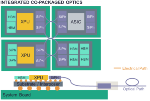
Silicon Photonics Meets AI: Co-Packaged Optics for Next-Gen Performance
Silicon photonics is not entirely new; it has powered telecommunications networks for years through pluggable transceivers that connect data centre racks. These proven systems use silicon photonic dies combined with separate lasers and micro-lens technologies packaged into modules that can be easily replaced if they fail.
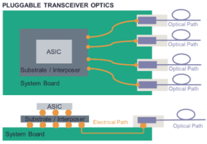
But AI’s demands are pushing photonics into uncharted territory. Instead of simply connecting separate systems, the technology must now integrate directly with processors, memory, and other components in what engineers call “co-packaged optics.” This approach promises to bring optical interconnects closer to the actual computation, maximising bandwidth while minimising energy consumption.
The challenge is reliability. While pluggable transceivers can be easily swapped out if they fail, co-packaged optical systems integrate directly with expensive graphics processors and high-bandwidth memory, making them a more reliable option. If an optical component fails in such a system, the repair becomes exponentially more complex and costly. Early implementations from major chip developers are still in pilot phases, carefully assessing long-term reliability before full-scale deployment.
Accelerating Adoption: How Industry Timelines Are Moving Faster Than Expected
Industry roadmaps that once projected capabilities for 2035 are already being met by leading manufacturers. The combination of urgent market need, massive investment, and three decades of accumulated photonics research has created what amounts to a perfect storm for commercialisation.
The implications extend far beyond data centres. As optical interconnects become more cost-effective and established, they have the potential to revolutionise everything from autonomous vehicles to edge computing devices. The same technology that enables sustainable AI scaling could ultimately transform how electronic systems communicate across virtually every application.
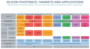 Source: Yole Group
The Future of Computing Is Optical Interconnects for Sustainable AI Growth
The question is how quickly it can be implemented and scaled. With leading manufacturers already investing billions and pilot systems entering data centres, the light-speed future of computing is no longer a distant possibility. Companies like Lam, through our customer-centric approach and advanced manufacturing solutions, enable this transformation by providing the precision tools that make commercial silicon photonics possible.
Silicon photonics represents a fundamental technology shift that could determine which companies lead the next phase of the digital revolution. Just as the introduction of copper interconnects enabled previous generations of performance scaling, optical interconnects have the potential to break through the barriers that threaten to constrain AI development.
For an industry grappling with the sustainability challenges of exponential AI growth, silicon photonics offers a path forward that doesn’t require choosing between performance and environmental responsibility. By replacing electrical inefficiency with optical precision, this technology could enable the continued advancement of AI while dramatically reducing its environmental footprint.
The revolution is just beginning, but one thing is clear: the future of high-performance computing is increasingly bright, and Lam is at the centre of it.
The post Silicon Photonics: The Lightspeed Revolution That Will Transform AI Computing appeared first on ELE Times.
AI-Augmented Test Automation at Enterprise Scale
Courtesy: Keysight Technologies
Enterprise test automation does not break because teams lack tools.
It breaks when browser-level automation is asked to validate systems far beyond the browser.
At enterprise scale, software quality depends on the ability to test entire user journeys across the full technology stack, from web and APIs to desktop, packaged applications, and highly graphical systems, without fragmenting tooling or multiplying maintenance effort.
This distinction explains why Keysight Technologies was positioned as a Leader in the 2025 Gartner Magic Quadrant for AI-Augmented Software Testing Tools, recognised for both Ability to Execute and Completeness of Vision.
Gartner defines AI-augmented software testing tools as solutions that enable increasingly autonomous, context-aware testing across the full software development lifecycle. In practice, that definition only matters if it holds up in complex, regulated enterprises.
One notable deployment is American Electric Power (AEP).
Why Browser-Only Automation Hits a Ceiling at Enterprise Scale
Most enterprises already use Selenium successfully for its intended purpose.
Browser automation works well when:
- The system under test is web-based
- Interactions are DOM-driven
- The scope is limited to UI flows
Problems emerge when enterprises attempt to extend browser-centric automation to validate full end-to-end systems that include:
- Highly graphical or non-DOM interfaces
- Desktop or packaged applications
- Field mobility tools and operational systems
- Integrated workflows spanning UI, APIs, and backend logic
At that point, teams are forced to stitch together multiple tools, frameworks, and scripts. The result is not resilience-it is complexity, fragmentation, and rising maintenance cost.
The issue is not Selenium.
The issue is using a single-layer tool to validate multi-layer systems.
What Gartner Means by AI-Augmented Software Testing
According to Gartner, the market is moving toward platforms that combine and extend automation capabilities, rather than replacing them.
Modern AI-augmented testing platforms are expected to:
- Orchestrate testing across UI, API, and visual layers
- Combine browser automation with image-based and model-based techniques
- Abstract complexity so teams test behaviour, not implementation details
- Reduce maintenance through models, self-healing, and intelligent exploration
- Scale across cloud, on-premises, and air-gapped environments
This is not an argument against existing tools.
It is recognition that enterprise testing requires a unifying layer above them.
Enterprise Reality: Complexity, Scale, and Risk at AEP
AEP operates one of the largest electricity transmission networks in the United States, serving 5.5 million customers across 11 states. Its software landscape includes:
- Customer-facing web applications
- Financial and billing systems
- Highly graphical, map-based field mobility applications
Before modernising its testing approach, AEP faced a common enterprise constraint:
- Browser automation covered part of the estate
- Critical operational systems remained difficult to validate
- Manual testing persisted in high-risk workflows
- Defects continued to escape into production
The challenge was not adopting another tool.
It was testing the full system end-to-end, consistently, and at scale.
How AEP Scaled Full-Stack, AI-Driven Testing
AEP began where confidence was lowest.
Rather than extending browser automation incrementally, the team selected a highly graphical, map-based field mobility application-a system that sat outside the reach of traditional browser-only approaches.
Using AI-driven, model-based testing, the application was automated end-to-end, validating behaviour across visual interfaces, workflows, and integrated systems.
That success changed internal perception.
As AEP’s Lead Automation Developer and Architect explained, proving that even their most complex system could be tested reliably shifted the conversation from “Can we automate this?” to “How broadly can we apply this approach?”
The key was not replacing existing automation, but extending it into a unified, full-stack testing strategy.
Measured Results: Time, Defects, and Revenue Impact
Once deployed across teams, the outcomes were measurable:
- 75% reduction in test execution time
- 65% reduction in development cycle time
- 82 defects identified and fixed before production
- 1,400+ automated scenarios executed
- 925,000 exploratory testing scenarios discovered using AI
- 55 applications tested across the organisation
- $1.2 million in annual savings through reduced rework and maintenance
In one instance, AI-driven exploratory testing uncovered 17 critical financial defects that had escaped prior to validation approaches. Resolving those issues resulted in a $170,000 revenue increase within 30 days.
This is not broader coverage for its own sake.
It is risk reduction and business impact.
Empowering Teams Beyond Test Engineers
Another enterprise constraint is who can contribute to quality.
At AEP, non-technical users were able to create tests by interacting with models and workflows rather than code. This reduced dependency on specialist automation engineers and allowed quality ownership to scale with the organisation.
Gartner highlights this abstraction as critical: enterprises need testing platforms that extend participation without increasing fragility.
What Enterprise Leaders Should Look for in AI Testing Platforms
The strategic question is not whether a tool supports Selenium.
The question is whether the platform can:
- Combine browser automation with visual, API, and model-based testing
- Validate entire user journeys, not isolated layers
- Reduce maintenance while expanding coverage
- Operate across the full enterprise application stack
- Scale trust before scaling usage
AEP’s experience illustrates Gartner’s broader market view: AI-augmented testing succeeds when it unifies existing capabilities and extends them, rather than forcing enterprises to choose between tools.
The Strategic Takeaway
Enterprise software quality now depends on full-stack validation, not single-layer automation.
Selenium remains valuable. But enterprise testing requires a platform that goes beyond the browser, orchestrates multiple techniques, and scales across real-world complexity.
Independent analyst research defines the direction. Real enterprise outcomes prove what works. AEP’s results show what becomes possible when AI-augmented testing is treated as a strategic, unifying capability. Not a collection of disconnected tools.
The post AI-Augmented Test Automation at Enterprise Scale appeared first on ELE Times.
Murata Launches New Tech Guide to Enhance Power Stability in AI-driven Data Centres
Murata Manufacturing Co., Ltd. has launched a new technology guide entitled: ‘Optimising Power Delivery Networks for AI Servers in Next-Generation Data Centres.’ Available on the company’s website, the guide introduces specific power delivery network optimisation solutions for AI servers that enhance power stability and reduce power losses across the data centre infrastructure.
The guide addresses the rapid advancement and adoption of AI, a trend driving the continuous rollout of new data centres worldwide. As the industry moves toward higher voltage operations and increased equipment density, the resulting increase in overall power consumption has made stable power delivery a critical business issue for data centre operators. Consequently, the guide focuses on power circuit design for data centres, providing a detailed overview of market trends, evolving technologies in power delivery, and the key challenges the sector currently faces.
To assist engineers and designers, the guide is structured to provide a market overview that breaks down power consumption and technology trends within power lines. It further addresses market challenges and solutions by examining key considerations in power-line design and exploring how the evolution of power placement architectures can facilitate power stabilisation and loss reduction.
Murata supports these architectural improvements with a broad product lineup that addresses advanced and evolving power delivery methods, including multilayer ceramic capacitors (MLCC), silicon capacitors, polymer aluminium electrolytic capacitors, inductors, chip ferrite beads, and thermistors. Furthermore, the company provides comprehensive design-stage support, using advanced analysis technologies to assist with component placement and selection. Backed by a robust global supply and support network, Murata continues to deliver tangible value by solving power-related challenges in data centres.
You can download the full technology guide here: Optimising Power Delivery Networks for AI Servers in Next-Generation Data Centres
The post Murata Launches New Tech Guide to Enhance Power Stability in AI-driven Data Centres appeared first on ELE Times.
Vishay Intertechnology launches New Commercial and Automotive Grade Power Inductors
Vishay Intertechnology, Inc. introduced four new power inductors in the 2.0 mm by 1.6 mm by 1.2 mm 0806 and 3.2 mm by 2.5 mm by 1.2 mm 1210 case sizes. The commercial IHLL-0806AZ-1Z and IHLL-1210AB-1Z and Automotive Grade IHLP-0806AB-5A and IHLP-1210ABEZ-5A achieve the same performance as the next-smallest competing inductor in 11 % (1210) and 64 % (0806) smaller footprints, while offering higher operating temperatures, a wider range of inductance values, and lower DCR for increased efficiency.
Offering inductance values from 0.24 µH to 4.70 µH and typical DCR down to 6.6 mΩ, the terminals of the IHLL-0806AZ-1Z and IHLL-1210AB-1Z are plated on the bottom only, enabling a smaller land pattern for more compact board spacing. The terminals of the IHLP-0806AB-5A and IHLP-1210ABEZ-5A are plated on the bottom and sides, allowing for the formation of a solder fillet that adds mounting strength against great mechanical shock, while simplifying solder joint inspection. The AEC-Q200 qualified devices provide reliable performance up to +165 °C, which is 10 °C higher than the closest competing composite inductor, and typical DCR down to 15.0 mΩ.
Delivering improved performance over ferrite-based technologies, all four devices feature a robust powdered iron body that completely encapsulates their windings — eliminating air gaps and magnetically shielding against crosstalk to nearby components — while their soft saturation curve provides stability across the entire operating temperature and rated current ranges. Packaged in a 100 % lead (Pb)-free shielded, composite construction that reduces buzz to ultra-low levels, the inductors offer high resistance to thermal shock, moisture, and mechanical shock, and handle high transient current spikes without saturation.
RoHS-compliant, halogen-free, and Vishay Green, the Vishay Dale devices released today are designed for DC/DC converters, noise suppression, and filtering in a wide range of applications. The IHLP-0806AB-5A and IHLP-1210ABEZ-5A are ideal for automotive infotainment, navigation, and braking systems; ADAS, LiDAR, and sensors; and engine control units. The IHLL-0806AZ-1Z and IHLL-1210AB-1Z are intended for CPUs, SSD modules, and data networking and storage systems; industrial and home automation systems; TVs, soundbars, and audio and gaming systems; battery-powered consumer healthcare devices; medical devices; telecom equipment; and precision instrumentation.
Device Specification Table:
| Series |
IHLL-0806AZ-1Z |
IHLP-0806AB-5A |
IHLL-1210AB-1Z |
IHLP-1210ABEZ-5A |
| Inductance @ 100 kHz (μH) |
0.24 to 4.70 |
0.22 to 0.47 |
0.24 to 4.70 |
0.47 to 4.70 |
| DCR typ. @ 25 °C (mΩ) |
16.0 to 240.0 |
15.0 to 21.0 |
6.6 to 115.0 |
18.0 to 150.0 |
| DCR max. @ 25 °C (mΩ) |
20.0 to 288.0 |
18.0 to 25.0 |
10.0 to 135.0 |
22.0 to 180.0 |
| Heat rating current typ. (A)(¹) |
1.3 to 6.3 |
4.6 to 5.8 |
2.3 to 9.2 |
1.8 to 5.1 |
| Saturation current typ. (A)(²) |
1.5 to 6.5 |
4.5 to 5.1 |
2.5 to 9.0 |
2.0 to 6.5 |
| Saturation current typ. (A)(³) |
1.8 to 7.2 |
5.4 to 7.5 |
2.9 to 11.5 |
2.5 to 8.2 |
| Case size |
0806 |
0806 |
1210 |
1210 |
| Temperature range (°C) |
-55 to +125 |
-55 to +165 |
-55 to +125 |
-55 to +165 |
| AEC-Q200 |
No |
Yes |
No |
Yes |
(¹) DC (A) that will cause an approximate ΔT of 40 °C
(²) DC (A) that will cause L0 to drop approximately 20 %
(³) DC (A) that will cause L0 to drop approximately 30 %
The post Vishay Intertechnology launches New Commercial and Automotive Grade Power Inductors appeared first on ELE Times.
Loom Solar Introduces Revolutionary, Scalable CAML BESS Solution up to 1 MWh to Replace Diesel Generators for C&I Sector
Loom Solar, one of India’s leading solar manufacturing companies, announced the launch of its scalable 125kW/261kWh CAML Battery Energy Storage System (BESS) up to 1MWh, a next-generation solution designed to deliver uninterrupted, seamless power tothe Commercial and Industrial (C&I) sector, significantly reducing production losses caused by power outages.
Unlike conventional diesel generator-based systems, which typically involve switch-over downtimes ranging from 30 seconds to 3 minutes, Loom Solar’s scalable 125kW/261kWh BESS ensures instantaneous power availability, eliminating operational disruptions in critical industrial processes. The system is engineered for a cleaner, quieter, and safer microgrid application that addresses low-voltage situations and power cuts while delivering continuous power for over two hours, with deep-discharge capability, making it a reliable alternative for businesses that demand high uptime and operational efficiency.
With a lifecycle of up to 6,000 charge–discharge cycles, the scalable 125kW/261kWh BESS offers long-term durability and superior economic value.
Developed through Loom Solar’s strong focus on in-house research and development, and validated through rigorous product testing facilities, the solution reflects the company’s commitment to innovation and reliability. The system is IoT-enabled and compatible with connected energy ecosystems, allowing real-time monitoring, intelligent energy management, and seamless integration with renewable power sources such as solar.
Commenting on the launch, Amod Anand, Co-Founder and Director, Loom Solar, said, “The scalable 125kW/261kWh BESS is a solution-led product designed specifically for India’s C&I sector, where even a few seconds of downtime can translate into significant losses. Our focus has been to replace reactive power backup with intelligent, seamless energy continuity. This solution not only ensures uninterrupted operations but also helps businesses optimise energy costs and move closer to energy independence through renewable integration.”
With this launch, Loom Solar strengthens its position as a key enabler of India’s energy transition, offering integrated solar and energy storage solutions that support energy security, sustainability, and long-term resilience for businesses.
The post Loom Solar Introduces Revolutionary, Scalable CAML BESS Solution up to 1 MWh to Replace Diesel Generators for C&I Sector appeared first on ELE Times.
Infineon strengthens its leading position in sensors acquiring non-optical analogue/mixed-signal sensor portfolio from ams OSRAM
Infineon Technologies AG is expanding its sensor business with the acquisition of the non-optical analogue/mixed-signal sensor portfolio from ams OSRAM Group. The two companies have entered into an agreement for a purchase price of €570 million on a debt-free and cash-free basis. With the planned investment, Infineon will strengthen its position as a leader in sensors for automotive and industrial markets through a complementary portfolio and expand its product range in medical applications. The acquired business is expected to generate around €230 million in revenue in calendar year 2026 and will support Infineon’s profitable growth. The transaction will be accretive to earnings-per-share immediately upon closing, with future synergies enabling substantial additional value creation. As part of the transaction, around 230 employees with expertise in research and development (R&D) and business management will join Infineon. The agreement includes a multi-year supply agreement with ams OSRAM.
“The acquired business is a perfect strategic fit for Infineon and complements our strong offering in the analogue and sensor space. We will be able to provide our customers with even more comprehensive system solutions,” says Jochen Hanebeck, CEO of Infineon. “I am convinced that this is an outstanding technological, commercial and cultural match, generating growth opportunities in our current target markets as well as in emerging areas like humanoid robotics.”
The overall transaction is structured as a fabless asset deal covering sensor products, R&D capabilities, intellectual property and test & lab equipment. The transaction is subject to customary closing conditions, including regulatory approvals, and is expected to close in the second quarter of calendar year 2026. Infineon will fund the acquisition with additional debt, as part of its general corporate financing plans.
Sensors are the link between the physical and the digital world, as they detect and convert signals such as movement, sound, light waves, temperature and even heartbeat and strain into processible data. They are at the core of a wide array of applications like software-defined vehicles, health trackers, and physical AI applications such as humanoid robots. The market potential of the sensor and radio frequency markets is projected to exceed $20 billion by 2027.
The acquired Mixed Signal Products business will add leading medical imaging and sensor interfaces to the portfolio of Infineon, including X-ray solutions and sensors used for valve control, building control technology and metering. The Positioning & Temperature Sensors assets will strengthen Infineon’s high-precision position, capacitive and temperature sensing for automotive, industrial and medical applications, such as chassis position sensing and hands-on detection in vehicles, angle and position sensing for robotics and glucose monitoring.
The acquisition fully supports Infineon’s strategy to grow its sensor business. Infineon established its Sensor Units & Radio Frequency (SURF) unit within its Power & Sensor Systems (PSS) division in January 2025. This aligns with the strategy to offer customers comprehensive system solutions through a powerful, interlinked portfolio in “analogue & sensors”, “power” and “control & connectivity”.
The post Infineon strengthens its leading position in sensors acquiring non-optical analogue/mixed-signal sensor portfolio from ams OSRAM appeared first on ELE Times.
The Rare Earths Catch-22: Why It Exists and How It Can Be Fixed
Speaking at the Auto EV Tech Vision Summit 2025, Bhaktha Keshavachara, CEO, Chara Technologies, highlights the Rare Earth challenges as faced by the world today and what potential policies can resolve them!
As the world strides towareds more sustainable solutions, the technologies we use become more rare-earth dependent, ranging from batteries to motors and the magnets used in the motors. To couple this phenomenon, a simultaneous energy transition is also taking shape. We are gradually moving towards achieving our energy goals from electrons, as compared to hydrocarbons previously, especially in transportation. This necessitates the need to locate supply chains in a stable region or wholly become self-sustainable in the raw materials, which are Rare Earths, the 17 elements put separately in the periodic table, as Bhaktha Keshavachara, CEO, Chara Technologies, puts it!
With Rare Earths, the global catch-22 lies for two specific reasons, namely:
- It is expensive to buy
- It is hazardous to extract
Since these materials are critical for our future, or the future dominated by Electric technologies like EVs, E-Buses, etc – It becomes imperative for us to search for ways to locate them in stable regions or make oneself self-sufficient in their production, or simply find ways. Let’s see what Bhaktha had to say about it!
Start Mining or Find Alternatives
“We have to start mining and extraction,” Bhaktha reiterates as he presents his first solution for the Rare-Earth catch-22. He goes on to recount the strategies adopted by the nations globally, including the US, which has interestingly reopened its mines in California for rare-earth minerals. Further, he underlines the ongoing global efforts to find alternative materials to build rare-earth magnets without using rare earths. He underlines NIRON from the US, which is experimenting with iron nitride magnets. He also points to Europe’s efforts towards finding an alternative in potassium-strontium magnets.
The problem with rare-earth mining is the hazardous nature of the process that leaves populations and people cancer-ridden for a long time. “If you see pictures on the net of the west coast of China, actually in central China, there are like cancer villages,” Bhaktha recounts.
Alternative Motor Technologies or Materials
Further, he suggests using alternative motor technologies to reduce the materials component of rare earths in the overall product. He refers to the various motor types in the same continuation, including electrically excited synchronous motors (EESM), induction motors (IM), and synchronous reluctance motors (SynRM). He also touches upon the light rare-earth materials, calling for more use of them as opposed to the heavy rare-earth materials that China holds a stronghold over, as he mentioned in his address
India’s Situation
Talking about India’s situation, Bhkatha says, “We have rare earths, but not all the 17 rare earths, but still we can do with whatever we have, and potentially we can import ore which has dysprosium and other rare earth materials.” He also recounts some past events wherein global price fluctuations anchored by China led to two big companies in India dropping projects of magnet manufacturing as the project suddenly became unviable in business terms.
In the same sequence, he reiterates the example of the US government that has stepped in to cap the minimum prices for the magnets irrespective of the global market fluctuations, to basically support the industry and also enable localisation of the technology and materials.
National efforts, Global Repercussions
In the midst of all these challenges, Bhaktha reaffirms his determination to face the storm in the face, calling upon the industry to innovate for the better. He says, “I think if we do the innovation and take the leadership role in prioritizing this, we not only have a huge opportunity to do something new in India, but there is a huge opportunity to export to the rest of the world because the rare-earth problem is a global problem.”
The post The Rare Earths Catch-22: Why It Exists and How It Can Be Fixed appeared first on ELE Times.
New Power Module Enhances AI Data Centre Power Density and Efficiency
The increasing AI and high-performance computing workloads demand power solutions that combine efficiency, reliability and scalability. Integrated power modules help streamline design, reduce energy use and deliver the stable performance required for advanced data centres. Microchip Technology announces the launch of the MCPF1525 Power Module, a highly integrated device with a 16V Vin buck converter that can deliver 25A per module, stackable up to 200A. The MCPF1525 enables higher power delivery within the same rack space and is combined with a programmable PMBus and I2C controls. This device is designed to power the latest generation of PCIe switches and high-performance compute MPU applications needed for AI deployments.
The MCPF1525 is packaged in an innovative vertical construction that maximises board space efficiency and can offer up to a 40% board area reduction when compared to other solutions. The compact power module is approximately 6.8 mm x 7.65 mm x 3.82 mm, making it an optimal solution for space-constrained AI servers.
For increased reliability, the MCPF1525 includes multiple diagnostic functions reported over PMBus, including over-temperature, over-current and over-voltage protection to minimise undetected faults. With a thermally enhanced package, the device is engineered to work within an operating junction temperature range of -40°C to +125°C. An on-board embedded EEPROM allows users to program the default power-up configuration.
“By leveraging Microchip’s comprehensive solutions, including PCIe Switchtec technology, FPGAs, MPUs and Flashtec NVMe controllers, the MCPF1525 power module can help customers achieve the system efficiency, reliability and scalability required for high-performance data centre and industrial computing applications,” said Rudy Jaramillo, vice president of Microchip’s analogue power and interface division. “Seamless integration across Microchip’s portfolio simplifies development and lowers risk, helping designers accelerate time-to-market.”
The MCPF1525 features a customised integrated inductor for low conducted and radiated noise, enhancing signal integrity, data accuracy and reliability of high-speed computing, helping reduce repeated data transmissions that waste valuable system power and time.
The post New Power Module Enhances AI Data Centre Power Density and Efficiency appeared first on ELE Times.
Budget 2026–27: How a Rare Earth Corridor Can Power India’s Electronics & Automotive Manufacturing Push
The Union Finance Minister Smt Nirmala Sitharaman unveils the Union Budget 2026-27 on the floor of the house, amidst India’s stride to capitalise on its electronics & IT sector while boosting its defence expenditure and technology both. The union budget proposes to establish a Rare-Earth Corridor in mineral-rich states, including Tamil Nadu, Andhra Pradesh, Odisha, and Kerala. The move is all set to benefit the automotive and electronics industriesby emans of ensuring a safe and self-sustainable rare-earth corridor to complement India’s upward momentum in automobile and electronics manufacturing.
The Union Budget 2026-27 makes some to-the-point and striking announcements to support the upward momentum in self-enablement and security within and across the borders, both.
What are Rare-earths Important?
As the world moves toward more sustainable solutions, the technologies driving this shift are becoming increasingly dependent on rare earth materials—from batteries and electric motors to the magnets that power them. Parallel to this trend, a global energy transition is also gaining momentum. With electric technologies such as EVs and e-buses set to dominate the future, these materials have become strategically critical. This makes it imperative to secure their supply—either by sourcing them from geopolitically stable regions or by building self-sufficiency across the rare earth value chain.
Quite Rare “Rare-Earth” Materials
As the name itself suggests, but geopolitics makes them far rarer. The challenge with rare-earth mining lies not only in scarcity but in the hazardous nature of the extraction process itself. Poorly regulated mining and processing have left long-term environmental and human health consequences, with communities exposed to toxic by-products for decades.
Recalling the impact, Bhaktha Keshavechara, CEO, Chara Technologies, pointed in his address at Auto EV TVS 2025 to the regions in central China where entire settlements have been affected—often referred to as “cancer villages”—underscoring the severe social cost embedded in the global rare-earth supply chain. Conversely, the recycling of the material is way costlier than the virgin material itself, making the equations way more difficult.
Easier logistics, Easier access
A dedicated corridor for rare earths would certainly make the rare-earth materials way more accessible across all of India, for either the electronics or the automotive industry. This ease in accessibility will manifest itself in the form of more research, more interaction with the materials to find more solutions, making the technology and development process accessible and grounded in the nation itself. Thai will pave the way for more innovations in this field.
National Efforts Unlocking Global Opportunity
The proposal would empower India’s position in the rare-earth value chain globally, as the problem currently engulfs the entire world. The initiative is expected to generate stronger local economies and enhance R&D capacity. This will integrate India more deeply into global advanced‑materials value chains, as dedicated access would make even exports easier.
Coupled with complementary international partnerships and institutional reforms, further ensure resilient access to critical minerals. With coordinated domestic and global initiatives, India is gradually positioning itself as a reliable and competitive player in advanced materials value chains.
The post Budget 2026–27: How a Rare Earth Corridor Can Power India’s Electronics & Automotive Manufacturing Push appeared first on ELE Times.
Element Solutions Completes Acquisition of Micromax Business
Element Solutions Inc (ESI) today announced the completion of its acquisition of the Micromax conductive pastes and inks business, effective February 2, 2026. Micromax will operate within MacDermid Alpha Electronics Solutions, part of ESI’s Electronics segment.
The acquisition strengthens ESI’s position as a leading global supplier of specialised electronic materials serving the electronics design and manufacturing industry. By combining Micromax’s expertise in conductive pastes, inks, and ceramic materials with MacDermid Alpha’s broad electronics materials portfolio, ESI expands its ability to support innovation across advanced and high-reliability electronics applications.
“The acquisition of Micromax is a strong strategic fit for ESI and reinforces our focus on high-value, technology-driven businesses,” said Richard Fricke, President, Electronics, adding, “Micromax’s differentiated materials and long-standing customer relationships further strengthen our Electronics segment and expand our ability to support innovation across the electronics manufacturing ecosystem.”
Building Breakthroughs by Leveraging Our Combined Expertise
With Micromax now part of MacDermid Alpha Electronics Solutions, customers gain access to a broader, highly complementary portfolio of advanced electronic materials designed to enable performance, reliability, and design flexibility. The combined portfolio includes thick-film conductive inks compatible with polymer films, glass tapes, metals, and ceramics, as well as Low Temperature Co-Fired Ceramic (LTCC) materials that support high multilayer circuit density and withstand extreme operating environments.
These materials are used in critical electronic functions, such as circuitry, interconnection, and packaging and serve a wide range of end-use markets, including automotive and advanced mobility, telecommunications/5G infrastructure, consumer electronics, aerospace and defence, and medical devices.
“Micromax brings highly complementary technologies and deep materials expertise that align naturally with MacDermid Alpha’s mission,” said Bruce Moloznik, Sr. VP Business Integration, MacDermid Alpha Electronics Solutions. “Together, we are building breakthroughs that help customers accelerate innovation, deliver high reliability, and compete with confidence in demanding electronics markets.”
The post Element Solutions Completes Acquisition of Micromax Business appeared first on ELE Times.
Worldwide IT Spending to Grow 10.8% in 2026, Amounting $6.15 Trillion, Forecasts Gartner
Worldwide IT spending is expected to reach $6.15 trillion in 2026, up 10.8% from 2025, according to the latest forecast by Gartner, Inc., a business and technology insights company.
“AI infrastructure growth remains rapid despite concerns about an AI bubble, with spending rising across AI‑related hardware and software,” said John-David Lovelock, Distinguished VP Analyst at Gartner. “Demand from hyperscale cloud providers continues to drive investment in servers optimised for AI workloads.”
Server spending is projected to accelerate in 2026, growing 36.9% year-over-year. Total data centre spending is expected to increase 31.7%, surpassing $650 billion in 2026, up from nearly $500 billion the previous year (see Table 1).
Table 1. Worldwide IT Spending Forecast (Millions of U.S. Dollars)
|
2025 Spending |
2025 Growth (%) |
2026 Spending |
2026 Growth (%) |
|
| Data Centre Systems | 496,231 | 48.9 | 653,403 | 31.7 |
| Devices | 788,335 | 9.1 | 836,417 | 6.1 |
| Software | 1,249,509 | 11.5 | 1,433,633 | 14.7 |
| IT Services | 1,717,590 | 6.4 | 1,866,856 | 8.7 |
| Communications Services |
1,303,651 |
3.8 |
1,365,184 |
4.7 |
| Overall IT | 5,555,316 | 10.3 | 6,155,493 | 10.8 |
Source: Gartner (February 2026)
Software Spending Shows Second-Highest Growth Potential Despite Lower Revision
Software spending growth for 2026 has been slightly revised downward to 14.7%, from 15.2% for both application and infrastructure software.
“Despite the modest revision, total software spending will remain above $1.4 trillion,” said Lovelock. “Projections for generative AI (GenAI) model spending in 2026 remain unchanged, with growth expected at 80.8%. GenAI models continue to experience strong growth, and their share of the software market is expected to rise by 1.8% in 2026.”
Device Growth Expected to Slow in 2026
Shipments of mobile phones, PCs, and tablets continue to grow steadily. Total spending on devices is projected to reach $836 billion in 2026. However, market-demand constraints will slow growth to 6.1% in 2026.
“This slowdown is largely due to rising memory prices, which are increasing average selling prices and discouraging device replacements,” said Lovelock. “Additionally, higher memory costs are causing shortages in the lower end of the market, where profit margins are thinner. These factors are contributing to more muted growth in device shipments.”
The post Worldwide IT Spending to Grow 10.8% in 2026, Amounting $6.15 Trillion, Forecasts Gartner appeared first on ELE Times.
Pages

