
ELE Times

WORKS Integration – the data center for intelligent manufacturing
ASMPT presents central platform for data exchange in electronics manufacturing.
“WORKS Integration ensures that all production data is available exactly where it is needed for things like production planning and setup preparation, material flow and process optimization, and quality control,” said Thomas Bliem, Vice President R&D at ASMPT SMT Solutions. “By creating a centrally networked database with high connectivity across all systems, the platform makes fully digitized and highly automated intelligent production possible.”
A central data hub for all systems
Extending across all protocols and versions, WORKS Integration establishes an IIoT communication base to which the sensors on the production hardware as well as all software applications send their data. In addition to connecting the entire hardware and software portfolio of ASMPT SMT Solutions, WORKS Integration makes it possible to integrate third-party machines and programs via industry-standard interfaces. Even complex customer-specific applications can be easily linked via proprietary interfaces.
All connected systems obtain the information they need exclusively via WORKS Integration. Operating in the background, the application enables the continuous exchange of data between different hardware and software entities irrespective of their format or manufacturer.
WORKS Integration supports proven internal machine interfaces as well as industry standards such as IPC-2591, CFX, and SECS/GEM. Adapters convert all incoming information into a shared public data structure.
Centralized, standardized, resilient
This unified system offers numerous advantages for users. Since the various instances do not communicate with each other directly but exclusively through WORKS Integration, the number of interfaces and data channels is reduced considerably, as are potential interdependencies and sources of errors.
Machines and/or programs can be easily replaced, updated and scaled up or down without creating version conflicts or redundant data streams while encrypted communication reliably protects the system from unauthorized access. In addition, a central health monitoring system provides valuable information for technical support and fault analysis.
The post WORKS Integration – the data center for intelligent manufacturing appeared first on ELE Times.
Rohde & Schwarz Satellite Industry Day 2025: Connecting the world with New Space and 5G NTN technologies
Rohde & Schwarz is hosting its fifth Satellite Industry Day on June 3, 2025. Rohde & Schwarz test and measurement experts and partners from the industry will present topics from 5G Non-Terresterial Network (NTN) and satellite testing to monitoring and regulatory issues
After the keynote speech from Rohde & Schwarz Executive Vice President Test & Measurement Christina Gessner, Reiner Stuhlfauth from Rohde & Schwarz discusses tackling the challenges of NTN evolution on the path to 6G, including technology aspects, challenges, and testing. His colleague Goce Talaganov focuses on ensuring 5G NTN device performance, presenting market trends, use cases, challenges, and test solutions.
Obilor Nwamadi from Viavi Solutions presents an end-to-end emulation system for evaluating NTN connectivity to guarantee return on investment before design or deployment.
Rohde & Schwarz expert Dr. Yvonne Weitsch explores testing and technologies for Electronically Steered Array (ESA) antennas in satellite and NTN integration, discussing their advantages and proposing test solutions.
Prof. Dr. Klaus Schilling from the Center for Telematics discusses the future of space with smarter, smaller, and more cooperative satellites, highlighting the shift to networked small satellites and innovative technologies for global connectivity.
Alexander Spaniol from Terma Technologies GmbH covers the transformative role of Software-Defined Radio (SDR) in advancing space technology, emphasizing its flexibility and role in satellite communications, testing, and ground stations.
Rohde & Schwarz expert Pia Feurstein talks about improving signal quality in satellite communication with antenna combining with the help of the R&S MSR4 multipurpose satellite receiver. Her colleague Jean-Pierre Messmer introduces Space Nexus, a software solution for end-to-end satellite link channel emulation to validate systems in a laboratory environment.
Uwe Baeder from Rohde & Schwarz discusses the regulatory framework for space communication, focusing on the ITU’s role, coordination procedures, evolving regulations, and key issues for WRC-2712.
The post Rohde & Schwarz Satellite Industry Day 2025: Connecting the world with New Space and 5G NTN technologies appeared first on ELE Times.
Vishay Intertechnology 80 V MOSFET in PowerPAK 8x8SW Package Offers Best in Class RDS(ON) of 0.88 mΩ to Increase Efficiency
Space-Saving Device Offers Low Max. RthJC of 0.36 °C/W and Wettable Flanks to Improve Thermal Performance and Solderability in Industrial Applications
To provide higher efficiency for industrial applications, Vishay Intertechnology, Inc. introduced a new 80 V TrenchFET Gen IV n-channel power MOSFET in the PowerPAK 8x8SW bond wireless (BWL) package with best-in-class on-resistance. Compared to competing devices in the same footprint, the Vishay Siliconix SiEH4800EW offers 15 % lower on-resistance while reducing RthJC by 18 %.
With on-resistance down to 0.88 mΩ typical at 10 V, the device released today minimizes power losses from conduction to increase efficiency while improving thermal performance with a low maximum RthJC of 0.36 °C/W. With its 8 mm by 8 mm footprint, the space-saving device occupies 50 % less PCB space than MOSFETs in the TO-263 package while offering an ultra-low profile of 1 mm.
The SiEH4800EW implements a fused lead to increase the source PAD solderable area to 3.35 mm², which is four times larger than a traditional PIN solder area. This decreases the current density between the MOSFET and PCB, reducing the risk of electro-migration risk and enabling a more robust design. In addition, the device’s wettable flanks enhance solderability while making it easier to visually inspect the reliability of solder joints.
The MOSFET is ideal for synchronous rectification and OR-ing functionality. Typical applications will include motor drive controls, power tools, welding equipment, plasma cutting machines, battery management systems, robotics, and 3D printers. In these applications, the device offers high-temperature operation to +175 °C, and its BWL design minimizes parasitic inductance while maximizing current capability.
RoHS-compliant and halogen-free, the MOSFET is 100 % Rg and UIS tested.
The post Vishay Intertechnology 80 V MOSFET in PowerPAK 8x8SW Package Offers Best in Class RDS(ON) of 0.88 mΩ to Increase Efficiency appeared first on ELE Times.
Unlocking India’s High-Tech Security Potential: R&S India MD Yatish Mohan on Localisation, Innovation & Market Momentum
In an energetic discussion with Yatish Mohan, Managing Director, India at Rohde & Schwarz (R&S), a vision stood out: fusing leading-edge global technology with India’s strategic priorities in localisation, innovation, and infrastructure development. With India speeding up its digitalisation and security upgrades, R&S is positioning itself at the center — not only as a supplier, but as a long-term ecosystem ally.
Localisation & Compliance: A Non-Negotiable PriorityIndia’s policy climate is changing fast, and R&S is perfectly in sync with it. With a mandatory 20% local content norm for every government tender, including through GeM and direct procurement channels, the company has designed its operational and supply chain models accordingly.
Their SKD (Semi-Knocked Down) assembly model, where RF modules and mechanical components are imported from Germany for final assembly in India, maintains high standards while ensuring compliance. Although the PLI scheme continues to be applicable, it is not yet a core thrust, with R&S continuing to ramp up its volumes in India.
Critically, local value addition goes beyond physical elements. R&S ensures that software development, integration, and IT infrastructure—from servers to PCs and switches—are locally sourced and installed. In defence and aerospace, where the level of scrutiny is even greater, the capacity to prove indigenous components and technologies is critical to tender wins.
Scaling Operational Capabilities in IndiaR&S already has a strong presence in India, covering sales, calibration, maintenance, R&D, IT support, and partial SKD manufacturing. Now, the emphasis is on scaling these functions—specifically sales, service, and application engineering—to address the burgeoning demand across industries.
Mr Mohan underscored the significance of developing local talent, technical and commercial. With its expansion, R&S is also investing in intensive training schemes for its customers and employees to build further product insights and improve long-term results.
Aviation Security & Industrial Development: Market Tectonics Are Shifting
India is becoming a hub for cutting-edge security technology, particularly in aviation security. R&S’s whole-body scanners have already passed successful pilots in Bangalore, Delhi, Hyderabad, Goa, and Cochin, and interest is picking up across embassies, parliaments, malls, and high-security auditoriums.
With airport traffic exploding and infrastructure growing fast under India’s civil aviation drive, the opportunity is obvious: high-throughput, high-accuracy security screening isn’t a luxury — it’s a necessity.
In the industrial space, major manufacturers of perfumes, jewellery, and precious metals are turning to technology to mitigate internal theft as well as provide better facility security. Again, here, Mohan observes a willingness to spend money on high-quality, tested technologies.
Product Strategy: Deep RF Expertise, Long-Term VisionR&S’s worldwide leadership lies in its core competence in RF and wireless Test instrument product ranges extend as high as 170 GHz, up to 330 GHz with frequency extension. The company is perennially among the top T&M manufacturers worldwide in different product segments, from general purpose oscilloscopes or signal generators and analyzers for applications in multiple industries down to the more specialised segments like EMC test equipment.
R&S considers itself a technology partner for the entire wireless communications ecosystem. Together with chipset suppliers, device and infrastructure OEMs, test houses and network operators, the company has enabled connectivity for generations up to 5G and will continue to do so with 6G and beyond. Solutions already address NTN and the new FR3 frequency range, a candidate for 6G, as well as technologies like Reconfigurable Intelligent Surfaces (RIS) and Integrated Sensing and Communications (ISAC), enabling the next generation of wireless communication.
Beyond wireless, R&S offers test solutions that cover all kinds of applications in electronics testing, making sure digital designs, power electronics, high-speed digital interfaces, RF and microwave components or medical devices meet the highest quality standards.
The solutions also address all trends in the automotive industry, like connectivity and infotainment systems, automotive radar or in-vehicle networks. And the aerospace and defense sectors rely on R&S test instruments. There are also strong relations within the global research and education community.
Privately owned and proudly independent, R&S has the luxury of long-term thinking. As Mohan puts it, “We invest in technologies that may not be profitable today, but are vital for the future.”
Building Ecosystem Trust: Beyond SalesR&S’s engagement strategy is wonderfully non-transactional. Their Technology Symposiums are not sales pitches — they’re forums for deep technology sharing, establishing trust throughout the ecosystem with participants such as CDOT, Qualcomm, Samsung, and top academic institutions.
Under this model, selling is a spin-off of honest cooperation and learning, not aggressive prospecting. There is also a change in mindset needed in India, Mohan says — especially when launching non-conventional applications of cutting-edge technology, like full-body scanners in civilian or commercial environments.
Rohde & Schwarz isn’t simply sending equipment to India — it’s inserting itself into India’s technology and security ecosystem. Through sophisticated localisation policy, an audacious talent programme, and an evident product and market strategy, the firm stands ready to contribute to shaping the high-tech destiny of India.
As Mohan concludes, “India is not just a market for us — it’s a strategic hub. We’re building for the long term.”
The post Unlocking India’s High-Tech Security Potential: R&S India MD Yatish Mohan on Localisation, Innovation & Market Momentum appeared first on ELE Times.
Top 10 Best Selling Android Phones in India
India’s smartphone market is among the most vibrant and competitive markets globally, with users constantly in search of the perfect balance of performance, innovation, and affordability. In 2025, top players such as Xiaomi, Samsung, Vivo, Oppo and Realme keep raising the tech bar with devices featuring new-generation processors, world class cameras, and fast charging technology. This article discusses the top 10 models that have drawn the attention of the Indian consumers, creating new standards for the mobile technology.
- Xiaomi 15 Ultra
Headquarter in Beijing, China, Xiaomi is best-known for high-performance smartphones that are competitively priced. The company emphasizes state-of-the-art camera technology, AI-based features, and quick-charging innovations. Xiaomi 15 Ultra is a power-packed flagship phone that is optimized for top-level performance and camera perfection.
Features:
Display: 6.73-inch LTPO AMOLED, 1440×3200 pixels, 120Hz
Processor: Snapdragon 8 Elite (3nm)
RAM & Storage: 12 GB/16GB RAM, 256GB/512GB/1TB storage
Camera: Quad setup (50 MP wide, 50MP telephoto, 200 MP periscope, 50MP ultrawide)
Battery: 5410mAh, 90W wired, 80W wireless charging
OS: Android 15 with HyperOS 2
- Samsung Galaxy S25 Ultra
Established in 1938, Samsung is a South Korean multinational corporation with headquarters in Suwon, South Korea. Samsung has grown to become one of the global technology giants, manufacturing state-of-the-art electronics, home appliances and smartphones. The Ultra variant from Samsung features a 6.9-inch Dynamic LTPO AMOLED 2 X screen, 200MP main camera, and One UI 7. It’s an expensive option for those seeking world-class performance.
Features:
Display: 6.9-inch Dynamic LTPO AMOLED 2X,1440×3120 pixels, 120Hz
Processor: Snapdragon 8 Elite (3nm)
RAM & Storage: 12GB/16GB RAM, 256GB/512GB/1TB storage
Camera: Quad configuration (200MP wide, 10MP telephoto, 50MP periscope, 50MP ultrawide)
Battery: 5000mAh, 45W wired, 15W wireless charging
OS: Android 15 with One UI 7
- Samsung Galaxy S25+
Just a bit less pricey than the Ultra, the S25+ maintains high-end specs, such as Snapdragon 8 Elite, 120Hz AMOLED screen, and speedy charging.
Features:
Display: 6.7-inch Dynamic AMOLED 2X, 1440×3120 pixels,120Hz
Processor: Snapdragon 8 Elite
RAM & Storage: 12GB RAM, 256/512GB storage
Camera: Triple setup (50MP wide, 10MP telephoto, 12MP ultrawide)
Battery: 4900mAh, 25Wwired, 15W wireless charging
OS: Android 15 with One UI 7
- Vivo X200 Pro
Established ijn 2009, Vivo is a Chinese technology brand that operates from its headquarters in Dongguan, China. The brand has become popular worldwide for its style-consious designs, high-end camera features, The Vivo X200 Pro is a professional-grade smartphone made for professional-level photography.
Features:
Display: 6.78-inch LTPO AMOLED, 1260×2800 pixels,120Hz
Processor: MediaTek Dimensity 9400 (3nm)
RAM & Storage: 16GB RAM, 256GB/512GB/1TB storage
Camera: Triple setup (50MP wide, 200 MP periscope, 50MP ultrawide)
Battery: 600mAh, 90W wired, 30W wireless charging
OS: Andriod with Funtouch OS 15
- Realme GT 6 Pro
Realme, with its headquarters in Shenzhen, China, is famous for budget-friendly yet high- performance smartphones with fast charging, AI-powered cameras, and gaming-centric features. Realme is famous for aggressive designs, top-notch performance, and flagship-grade features without the premium price. The Realme GT 6 Pro model is a high-end flagship phone built for speed, gaming.
Features:
Display: 6.78-inch LTPO AMOLED, 1264×2780 pixels, 120Hz
Processor: Snapdragon 8s Gen 3 (4nm)
Camera: Triple setup
Battery: 5500mAh, 120W wired charging
OS: Android 14 with Realme UI 5.0
- OnePlus 13
OnePlus, established in Shenzhen, China, is renowned for high-end flagship phones with seamless OxygenOS, Hasselblad-optimized cameras and rapid charging. OnePlus 13 is a high-end flagship smartphone filled with high-end feature and performance.
Features:
Display: 6.82-inch LTPO AMOLED, 1440×3168 pixels, 120 Hz
Processor: Snapdragon 8 Elite(3nm)
RAM & Storage: 12GB to 1 TB storage
Battery: 6000mAh, 100W wired, 50W wireless charging
- Oppo Find X7 Ultra
Oppo, headquartered in Dongguan, China, is a leader in camera technology, providing high-resolution photography, AI-driven photography. With emphasis on design, camera technology, and rapid charging, Oppo is a company that keeps innovating, resonating with consumers who desire beautiful yet powerful devices.
Features:
Processor: Snapdragon 8 Gen 3 (4nm)
RAM & Storage: 12GB to 512GB storage
Battery: 5000mAh,100W wired, 50W wireless charging
OS: Android 14 with ColorOS 14
- Google Pixel 9 Pro
Google, with its headquarters in Mountain View, California, USA, manufactures Pixel phones with stock Android experience, AI-driven photography, and proprietary software features. Google’s Pixel series is renowned for its stock Android experience, unparalleled camera software and AI-driven optimizations, so users can experience, AI-driven photography, and proprietary software features.
Features:
Display: 6.3-inch LTPO OLED
Processor: Google Tensor G4
RAM & Storage: 16GB RAM to 1 TB storage
Camera: Triple arrangement (50MP wide,48MP periscope, 48MP ultrawide)
Battery: 4700mAh, wired 27W, wireless 21W charging
- Motorola Edge 50 Ultra
Motorola, which was initially established in Chicago, USA, is currently owned by Lenovo (China). It specializes in rugged smartphones, pure Android experience, and AI-powered security features. Motorola Edge 50 Ultra comes with premium design, Snapdragon 8 Elite, and AI-powered security features.
Features:
Display: 6.7-inch P-OLED, pixels 1220×2712, 144Hz
Processor: Snapdragon 8s Gen(4nm)
Battery: 4500mAh, 125W wired, 50W wireless charging
- iQOO
Owned by Vivo, iQOO goes after performance-driven users who requires speed, gaming performance, and the latest hardware at a price that’s aggressively priced. iQOO deals in gaming smartphones with high-refresh-rate screens, high-performance chipsets and advanced cooling. iQOO, a gaming monster has a Snapdragon 8 Elite, 144Hz AMOLED screen and 6000mAh battery.
Features:
Display: 6.78-inch AMOLED
Camera: Dual setup (50MP wide, 8MP ultrawide)
Battery: 6400mAh, 80W wired charging
OS: Android 15 with Funtouch OS 15
|
|
||
|
Smartphone |
Market Price |
Trend |
|
Xiaomi 15 Ultra |
₹1,09,998 | Growing demand for camera-centric flagships |
|
Samsung Galaxy S25 Ultra |
₹1,06,000 |
Premium flagship supremacy |
|
Samsung Galaxy S25+ |
₹89,999 |
Budget flagship option |
|
Vivo X200 Pro |
₹84,999 |
Robust camera performance |
|
iQOO Neo 10R |
₹54,999 |
Gaming device |
|
Realme GT 6 Pro |
₹49,999 |
Performance-oriented flagship |
|
OnePlus 13 |
₹79,999 |
Oxygen OS and Hasselblad cameras |
|
OppoFind X7 Ultra |
₹76,000 |
Camera innovation |
|
Google Pixel 9 Pro |
₹95,999 |
AI-powered photography |
|
Motorola Edge 50 Ultra |
₹72,999 |
Premium design & security |
Conclusion:
India’s smartphone market continues to be extremely competitive with Android smartphones leading in sales. Vivo, Xiaomi and Samsung continue to top the market with high demand for features with AI, 5G connectivity, and flagship premium devices. Domestic smartphone manufacturing is increasing, lowering import dependence and enhancing the contribution of India as a primary production base for international brands. India’s smartphone market is likely to cross $100 billion, cementing its ranking among the world’s largest and fastest-expanding mobile markets, with more than 150 million smartphones expected to be shipped in 2025.
The post Top 10 Best Selling Android Phones in India appeared first on ELE Times.
Top 10 CPU Brands in USA
The speed, efficiency and overall performance of any computing device are all measured by its CPU (central processing unit). A few of the most popular CPU brands, which have made unique inventions and contributed to market value, are headquartered in the USA. Below is an overview of the top 10 CPU brands in the USA, including their popular models.
- Intel
The Santa Clara, California, headquartered semiconductor giant Intel was founded in 1968 and is framed for its powerful Core and Xeon processors that have enabled it to maintain a dominant market share.
Popular Model:
Intel Core i9 -14900k – 24 cores (8P+ 16E), 32 threads, boost clock up to 6.0 GHz, Intel Thread Director, PCle Gen 5 support.
Intel Core Ultra 9 285K – Processing with AI, 24 cores, 24 threads, 5.7 GHz boost clock, PCle Gen 5 support.
Intel Xeon W9-3495X – Workstation grade, 56 cores, 112 threads, high-performance computing.
- AMD
AMD is short for Advanced Micro Devices, was founded in 1969 and has its corporate headquarters in Santa Clara, California. Its Ryzen and EPYC processors are favorites in high-performance computing and gaming.
Popular Model:
AMD Ryzen 9 9950X – 16 cores, 32 threads, 5.7 GHz boost, 3D V-Cache tech, PCle Gen 5 compatibility.
AMD Ryzen 7 9800X3D- 8 cores, 16 threads, 5.2GHz boost, tuned for game performance.
AMD EPYC 9754 – Server grade CPU, 128 cores, 256 threads, data center intent.
- Qualcomm
Qualcomm is headquartered in San Diego, California and is a global leader in the mobile industry. Its Snapdragon CPUs are the brains of smartphones and tablets across the globe.
Popular Model:
Snapdragon 8 Gen 3 – ARM architecture, AI-optimized processing, 5G capabilities, Adreno GPU for visuals.
Snapdragon X Elite – 12 high-performance CPU core, AI-based computing, 45 Tops NPU performance.
Snapdragon 8cx Gen 4 – Engineered for Windows laptops, AI-driven efficiency, ultra-low power consumption.
- Apple
Apple, based in Cupertino, California, develops its own in-house M-series processors such as the M3 Pro and M3 Max that drive MacBooks and Mac desktops. These chips are recognized for their seamless integrations with macOS, offering high performance, energy efficiency and advanced GPU capabilities optimized for creative and professional workloads.
Popular Models:
Apple M3 Pro – 12-core CPU, 18-core GPU, optimized for macOS.
Apple M3 Max – Up to 16 CPU cores, 40 GPU cores.
- NVIDIA
NVIDIA has its headquarters in Santa Clara, California, USA. It was established in 1993 and has evolved into a worldwide leader in graphics processing units (GPUs), artificial intelligence (AI) hardware, high-performance computing and data center CPUs, such as the Grace Hopper and tegra families.
Popular Model:
NVIDIA Grace Hopper CPU – Server-class, AI processing
Tegra X1+ – Used in consoles such as Nintendo Switch
- IBM
IBM, Armonk, New York is legacy tech titan famous for its enterprise-level processors, specifically in mainframes and high-performance computing. IBM POWER and z-series processors are very popular among data centers, cloud computing and AI workloads.
Popular Models:
IBM Power10 – 15-core, high security enterprise CPU
IBM z16 – Mainframe chip, for banking and analytics
- Marvell Technology
Santa Clara, California, based Marvell Technology is a cloud-optimized and networking- centric CPU specialist with scalable ARM-based solutions like ThunderX3 and OCTEON for data centers.
Popular Models:
ThunderX3 – 96-core ARM CPU for data centers.
OCTEON 10 – 5nm AI-optimized networking chip.
- SiFive
San Mateo, California- based SiFive is a top player in RISC-V architecture, with high-performance, customizable CPUs for many applications, such as embedded systems and data centers.
Popular Models:
Performance P670 – Efficient edge device RISC-V core with high performance
Intelligence X280 – AI inference processing for AI applications.
- Ampere Computing
Santa Clara, California, based Ampere Computing creates ARM-based server processors such as Altra Max and AmpereOne, designed to provide performance along with power savings in contemporary clouds.
Popular Models:
Ampere Altra Max – 128-core ARM CPU
AmpereOne – Cloud-native CPU for next-generation systems
- Tenstorrent
Austin, Texas, based Tentorrent is a high-performance and AI company that designs RISC-V CPUs and AI accelerators. It is headed by Jim keller, a highly acclaimed chip architect. The company is looking to transform AI computing by combining high-performance CPUs and AI accelertors.
Popular Models:
Wormhole & Black Hole – High throughput AI datacenter CPUs
|
Brand |
Price Range |
| Intel | $460-$7,103 |
| AMD | $519-$4,998 |
| Qualcomm | $849-$1,598 |
| Apple | $1,499-$2,899 |
| NVIDIA | $42,500 |
| IBM | $41,00-$135,300 |
| Ampere Computing | $2,299-$5,000+ |
Conclusion:
Intel and AMD lead the CPU markets, with their extensive lines of processors designed to support gaming, professional use cases and business applications. Qualcomm leads the space for mobile computing with Snapdragon chips optimized for artificial intelligence-based computing. Apple uses a high-end pricing model for its M-series chips, optimized for integration in macOS. NVIDIA and IBM are also interested in high-performance computing, AI processing and enterprise-level solutions like Grace Hopper and Power10 CPUs. Marvell, SiFive, Ampere and Tenstorrent are new entrants dealing with cloud computing, AI acceleration and RISC-V architecture, but their pricing details for processors are limited.
The post Top 10 CPU Brands in USA appeared first on ELE Times.
Redefining Semiconductor Excellence: India Sets the Stage with 3nm Designs
With the launch of its very first 3nm chip design facilities in Noida and Bengaluru, India has made a significant leap in semiconductor technology. These cutting-edge facilities were inaugurated by the Ministry of Electronics & Information Technology (MeitY), led by Union Minister Ashwini Vaishnaw, marking a new era in India’s semiconductor sector.
A Notable Milestone in India’s Semiconductor Sector
Renesas Electronics India’s newly established 3nm chip design centres are a milestone for India’s semiconductor technology. Previously India worked on 7nm and 5nm chip designs, but with the change to 3nm technology, the country is among the global leaders in semiconductor technology.
Vaishnaw emphasized that designing at 3nm is truly next-generation, highlighting India’s growing expertise in semiconductor design. The Noida facility, in particular, is expected to play a crucial role on developing a pan- India semiconductor ecosystem, leveraging the country’s skilled workforce. He emphasized the industry’s increasing confidence by pointing to large investments firms like Applied Materials and Lam Research.
Government Strategy and Industry Investments
India’s chip roadmap stretches beyond design, to fabrication, advanced packaging (ATMP), equipment and material supply chains. In developing a self-dependent and globally competitive semiconductor ecosystem, the government is encouraging strategic collaborations, infrastructure development and home-grown innovation.
As part of further enhancing the talent pipeline, Vaishnaw launched a new semiconductor learning kit that was designed to impart engineering students with practical exposure in hardware design. More than 270 educational institutions that are already utilizing cutting-edge EDA (Electronics Design Automation) tools under the India Semiconductor Mission (ISM) will now be provided with these kits.
“Renesas Electronics, CEO, Hidetoshi Shibata, appreciated India’s growing influence in embedded systems as well as semiconductor innovation and said that Indo-Japan strategic partnership would be instrumental in shifting the semiconductor trend globally.”
Conclusion:
India’s opening of 3nm chip design hubs is a landmark moment in the country’s semiconductor journey, placing the country among the world leaders in the field of chip innovation. With its government-supported semiconductor strategy taking root, India is now moving beyond chip design to fabrication, advanced packaging (ATMP) and the materials supply chains, creating a sustainable semiconductor ecosystem.
The post Redefining Semiconductor Excellence: India Sets the Stage with 3nm Designs appeared first on ELE Times.
India’s Semiconductor Push: Renesas-CG Power JV to Debut First Chip by 2026
In a major step towards strengthening India’s semiconductor manufacturing base, Murugappa Group firm CG Power and Industrial Solutions Ltd. has joined hands with Japan’s Renesas Electronics Corporation and Thailand’s Stars Microelectronics to set up an Outsourced Semiconductor Assembly and Test (OSAT) plant in Sanand, Gujarat. The joint venture (JV) plans to launch its first chip from a pilot production line by mid-2026, said Renesas CEO Hidetoshi Shibata.
The JV will invest ₹7,600 crore in five years, funded by a combination of subsidies, equity, and possible borrowings from banks.
CG Power will have a 92.3% shareholding, while Renesas and Stars Microelectronics will have about 6.8% and 0.9%, respectively.
The Sanand plant is set to build up to a capacity of 15 million units a day, manufacturing various semiconductor packages. These comprise traditional packages such as Quad Flat No-Lead (QFN) and Quad Flat Package (QFP), and newer packages such as Flip Chip Ball Grid Array (FC BGA) and Flip Chip Scale Package (FC CSP). The offerings will serve different sectors, including automotive, consumer electronics, industrial, and 5G technology. This initiative aligns with India’s broader strategy to enhance its semiconductor ecosystem and reduce dependence on imports. The Union Cabinet approved the project under India’s Semiconductor scheme on February 29, 2024.
“Renesas CEO Hidetoshi Shibata emphasized that India must focus on building its intellectual property (IP) to boost its competitiveness in the international semiconductor industry.”
Conclusion:
The partnership combines the manufacturing experience of CG Power, Renesas’s cutting-edge semiconductor technology, and Stars Microelectronics’ knowledge in legacy package technology as well as training. As India further develops its semiconductor expertise, the joint venture represents a turning point towards making the nation a leader in the manufacture of chips worldwide. The partnership between Renesas, CG Power and Stars Microelectronics creates the potential for innovation, economic development and technological advancement in India’s semiconductor industry.
The post India’s Semiconductor Push: Renesas-CG Power JV to Debut First Chip by 2026 appeared first on ELE Times.
India’s Semiconductor Expansion: Jewar Facility Set to Boost Chip Production
The Union Cabinet has given clearance to a ₹3,706 crore semiconductor facility in Jewar, Uttar Pradesh, in a major boost to India’s semiconductor manufacturing plans. The facility, a joint initiative of HCL and Foxconn, will help consolidate India’s position in the international chip business.
The semiconductor plant will be set in the ‘Yamuna Expressway Industrial Development Authority’ (YEIDA) area, in the vicinity of the new ‘Noida International Airport’. This makes it easy to have uncontested connectivity and access to necessary infrastructure facilities, making it a most convenient location for semiconductor manufacturing.
The facility will concentrate on producing display driver chips, which are important parts used in mobile phones, laptops, automobile and other electronics. With its ability to produce 20,000 wafers per month, the plant is expected to be a significant player in India’s expanding electronics industry.
Economic Implication:
It is estimated that the semiconductor plant will provide around 2,000 job opportunities, which will offer highly qualified personnel with experience in the electronics and semiconductors industries. It’s also expected that the project will draw additional funding, which will enhance technological growth and development in the region.
The India Semiconductor Mission (ISM) has been actively encouraging indigenous production of chips and the plant is the sixth semiconductor manufacturing plant to be given approval under the scheme.
With the plant slated to go on stream by 2027, its contribution to job creation, technological innovation and economic growth will be substantial.
Conclusion:
The HCL- Foxconn chip manufacturing factory in ‘Jewar’ is an important milestone towards India’s path to self-sufficiency in making chips. The facility is constructed to produce 20,000 wafers per month and 36 million chips a month.
With the manufacture of display driver chips for the applications across many sectors, the plant will strengthen indigenous supply chains, decrease imports and enhance the country’s share in the international semiconductor industry.
The partnership between HCL and Foxconn demonstrates faith in India’s potential, opening doors for further innovation and investments in semiconductor production. As India continues to invest in semiconductor facilities, this move reaffirms its commitment to positioning itself as a global leader in the electronics sector.
The post India’s Semiconductor Expansion: Jewar Facility Set to Boost Chip Production appeared first on ELE Times.
Vishay Intertechnology Automotive Grade, SMD Thick Film Power Resistor Offers Enhanced Protection Against Short Transient Pulses
Offered in TO-263 (D²PAK) Package, Device Combines High Pulse Absorption to 15 J/0.1 s With Power Dissipation of 35 W
Vishay Intertechnology, Inc. announced that it has extended its D2TO35 series of surface-mount thick film power resistors with a new AEC-Q200 qualified device that delivers higher pulse absorption up to 15 J/0.1 s. Offered in the TO-263 (D²PAK) package, the Vishay Sfernice D2TO35H provides high power dissipation of 35 W at a +25 °C case temperature.
The Automotive Grade device released today features a unique design that provides 30 % higher energy absorption than the standard D2TO35 resistor for enhanced protection against short transient pulses. The result is more stable operation in high stress environments, reducing the risk of failure and improving overall system reliability while requiring fewer components to save board space, simplify layouts, and reduce overall solution costs.
The D2TO35H offers high temperature operation to +175 °C; a broad range of resistance values from 1 Ω to 14 kΩ, with tolerances down to ± 2 %; and thermal resistance of 4.28 °C/W. The device will serve as the active discharge, discharge, or precharge resistor for controls, 48 V board nets, BMS, fuel cells, and on-board chargers for HEVs, EVs, and low speed electric vehicles; energy monitoring and metering systems; agricultural vehicles and farm equipment; industrial motor drives, welding equipment, and power tools; and military weapons guidance systems.
The RoHS-compliant resistor offers a non-inductive design and is solder reflow secure at 270 °C/10 s.
The post Vishay Intertechnology Automotive Grade, SMD Thick Film Power Resistor Offers Enhanced Protection Against Short Transient Pulses appeared first on ELE Times.
Why the Future of Mobility Depends on Smarter, Smaller Semiconductors
Semiconductors are the crucial parts of electric vehicles (EVs) because they allow for advanced interactive features, efficiency battery management, powertrain enhancements and safety measures. The EV revolution is not only coming; it is currently happening. Semiconductors, a sometimes disregarded yet crucial building element, are the key element of this revolution. These microscopic semiconducting chips are the brain and nervous system of EVs, driving everything from power conversion and battery management to safety systems and intelligent infotainment systems. As EV adoption increases worldwide, demand for high-performance semiconductors is also on the rise making the EV semiconductor market one the most vibrant parts of the tech-led economy.
Market Overview:
Over the last few years, the EV semiconductor industry has seen enormous growth. Based on industry reports, global market size stood at approximately $11.19 billion as of 2023 and is expected to boom to nearly $57.1 billion by 2029 with a CAGR of more than 31%. The boom is being fueled by a combination of factors: tighter environmental controls, government subsidies, growing EV infrastructure and advances in automotive electronics technology.
EVs need significantly more semiconductor devices compared to conventional internal combustion engine (ICE) cars. From motor control units and battery management units (BMUs) to infotainment systems and advanced driver-assistance systems (ADAS), semiconductors make these features functional.
Key Technologies Driving Growth
Among the most prominent trends driving the market is the trend towards wide-bandgap semiconductors, specifically Silicon Carbide (SiC) and Gallium Nitride (GaN) materials. These materials are superior to conventional silicon for high-temperature and high-voltage applications and hence, they are suited for EV powertrains as well as rapid-charging infrastructure.
SiC chips, for instance, have the potential to make inverters more efficient, thus extending driving ranges and cutting energy loss. Players such as STMicroelectronics, Infineon, Wolfspeed and ON Semiconductor are investing heavily in SiC lines to address this increasing demand.
Since they allow producers to integrate several functions into a single chip and reduce the size and weight of their parts, system on chip (SoC) solutions are gaining popularity as well. This enhances overall car performance and design versatility.
Uses:
- In EVs, semiconductors are crucial to the vehicle’s battery management system (BMS). They assist in keeping an eye on the battery pack’s temperature, health and charge level. Onboarding charging systems also use semiconductors to help convert and control voltage, which improves charging speed and efficiency.
- Advanced driver assistance systems (ADAS) based primarily on semiconductor processors are adaptive cruise control, lane-keeping assist, and collision avoidance systems. These circuits make decisions in real time using data from multiple sensors, cameras, and radar.
- Infotainment systems are driven by semiconductor chips, incorporating features such as touchscreen display, GPS navigation, car audio, and connectivity features of the smartphone.
- As the largest, with more than half of the market, is the powertrain segment. Power semiconductors control battery power so that the electric motor can operate efficiently.
Regional Perspectives: Asia-Pacific Leads
Geographically, South Korea, Japan and China dominate the Asia-Pacific EV semiconductor market.
With schemes such as “Make in India” and the FAME II scheme (Faster Adoption and Manufacturing of Hybrid and Electric Vehicles) encouraging domestic EV and semiconductor manufacturing, India is also becoming a key player.
In addition to that, Europe is also deeply investing in environmental-friendly transport as well as in semiconductor technology. With the CHIPS and Science Act, America is also strengthening its domestic production of semiconductors to try to meet its demand less on foreign chipmakers and foster a stronger EV ecosystem.
Challenges and Supply Chain Constraints
Though there is a strong growth prognosis, the market does not lack its challenges. The most critical of these is the semiconductor supply chain crisis that commenced with the onset of the COVID-19 pandemic and has since impacted industries across the globe. The highly concentrated nature of chip production—dominated by just a handful of foundries such as TSMC (Taiwan) and Samsung (South Korea)—creates vulnerabilities.
Furthermore, geopolitical tensions, most notably between the U.S. and China, are recasting global trade patterns. China’s dominance of the supply chain of rare earth minerals like gallium and germanium, critical to semiconductor manufacturing, constitutes a strategic risk for the West and has fueled demands for diversification of sources.
Market volatility is also a problem. For example, firms such as Mersen and STMicroelectronics have recently pushed back their semiconductor revenue targets owing to volatile EV demand and postponed ramp-up of new plants. Analysts now estimate that key financial milestones will be achieved by 2029–2030, rather than previous estimates of 2026–2027.
Conclusion:
The EV Semiconductor industry sits at the confluence of mobility digitalization and transport electrification, with the demand growing at an unprecedented level. Recent data indicates that the sales of EVs worldwide will surpass 20 million units by 2025, representing one in four automobiles sold globally. The growth is fueled by heightened affordability, decreased operating expenses and government support.
Further, the market for compound semiconductor materials, comprising Silicon carbide (SiC) and Gallium Nitride (GaN) is estimated to increase from $29.97 billion in 2025 to $91.03 billion in 2025, driven by the growth of 5G and EV adoption. The overall semiconductor market is estimated to be $ 697 billion in 2025, representing an 11% year-over year growth rate.
Despite supply chain risks and market instability, improvements in production, materials and system integration will continue to advance the field. Technology specialists, investors, and manufacturers view this industry as having a high rate of return and playing a key role in shaping the direction of mobility in the future.
The post Why the Future of Mobility Depends on Smarter, Smaller Semiconductors appeared first on ELE Times.
Transforming Chip Design with Agentic AI: Introducing Cadence Cerebrus AI Studio
The industry’s first agentic AI, multi-block, multi-user SoC design platform.
Cadence has launched Cadence Cerebrus AI Studio. It is the industry’s first agentic AI multi-block multi-user design platform, significantly accelerating an entire system-on-chip’s (SoC) time to market by 5X.
Recent technological advancements have led to semiconductor chips with intricate functionalities requiring trillions of transistors. These chips must support high-performance computing and be designed using advanced process nodes. Cadence Cerebrus AI Studio is a state-of-the-art SoC agentic AI design implementation tool that can help achieve ambitious power, performance, and area (PPA) goals and reduce turnaround time for highly sophisticated chips.
Cadence Cerebrus AI Studio is aligned with Cadence’s Intelligent System Design strategy. For block-level AI-driven optimization, Cadence Cerebrus Intelligent Chip Explorer was released in 2021 and has successfully been used in hundreds of production designs. Cadence Cerebrus AI Studio is the next generation of AI-driven digital implementation products using the most advanced agentic AI technology for implementing an entire SoC or subsystem, enabling a generational shift from multiple designers optimizing a single block to multiple blocks being designed by a single engineer.
Utilizing the latest agentic AI system that features autonomous AI agents capable of making decisions and taking multi-step actions based on high-level objectives, Cadence Cerebrus AI Studio can orchestrate the complete chip implementation flow delivering engineering productivity benefits. The Innovus integrated RTL synthesis and implementation platform, including Python scripting and a large language model (LLM) AI assistant, provides completely automated design realization.
Key features of Cadence Cerebrus AI Studio include:
- Intelligent Agentic AI Workflows: Employs AI agents that manage design optimization methodologies, resulting in unparalleled PPA and accelerated design closure.
- Multi-Block, Multi-User Design Infrastructure: A central design platform empowers a single engineer to design multiple blocks, allowing for more µm2 of SoC implementation per engineer.
- Hierarchical Design Optimization: Top-block co-optimization using AI greatly reduces manual work and enables faster design closure.
- Advanced Data Analytics: AI-driven data platform facilitates smarter and faster design debug by quickly identifying bottlenecks and critical paths.
- Customizable Live Dashboard: Facilitates collaboration and knowledge sharing across designs and projects, resulting in exponential productivity benefits.
“We are thrilled to launch Cadence Cerebrus AI Studio, the industry’s first agentic AI SoC design platform, built on the solid foundation of established Cadence digital implementation tools. This tool extends the AI technology to hierarchical SoC design implementation, exponentially multiplying the PPA and productivity gains while addressing the engineering workforce shortage,” says Chin-Chi Teng, senior vice president and general manager, Digital & Signoff Group at Cadence. “Cadence Cerebrus AI studio, which leverages the latest agentic AI technology, is very well equipped to achieve unparalleled PPA, fastest time to design targets, and game-changing engineering efficiency.”
The post Transforming Chip Design with Agentic AI: Introducing Cadence Cerebrus AI Studio appeared first on ELE Times.
Keysight and SPHEREA Join Forces to Strengthen European Aerospace and Defense Testing Capabilities
- Provides access to strategic sovereign European programs with EU-designed, EU-built systems
- Enables locally developed solutions that are trusted, modular, and interoperable
- Integrates critical modular technology that enables next-generation measurement capabilities
Keysight Technologies, Inc. has collaborated with SPHEREA to offer customers improved testing capabilities in the aerospace and defense (A&D) sector. By joining forces, Keysight will combine its expertise in high-performance electronics tests and measuring systems with SPHEREA’s design and integration capabilities, to support the shifting requirements in the A&D space.
As European nations increasingly prioritize defense independence and aim to remain compliant with stringent export control regulations, this collaboration offers a timely and strategic response to these needs. The deployment of next-generation measurement technologies is critical to national security, but it is also essential to align with the need for EU-designed solutions to support self-sufficient and strategic autonomy.
Keysight and SPHEREA are working together to address this challenge, providing customers with local solutions that are built on trusted technology. As part of the agreement, the deployment includes the delivery of Keysight’s Radar Target Generator and Electronic Warfare testing solutions, featuring frequency expansion from 18 GHz to 40 GHz, which led to a successful tender for a leading military alliance. The solution consists of Keysight’s AXIe-based high-performance embedded controller with low latency and signal processing, arbitrary waveform generation, and its latest low phase-noise synthesizers.
“Our partnership with SPHEREA enables us to deliver an innovative, scalable solution. The accurate radar test solution is designed with our European R&D expertise, and delivery capabilities to provide future-ready tests that meet the evolving needs of our defense customers,” said Thierry Locquette, EMEA VP and GM at Keysight.
“We are proud to cooperate with Keysight using our deep RF expertise to develop the commercial off the shelf (COTS) Up and Down Converter with 1 GHz bandwidth in a short time frame. Together, we fulfilled the customer’s needs for advanced capability within a condensed timeline,” said Julien Pulice, Group CTO Deputy at SPHEREA.
The post Keysight and SPHEREA Join Forces to Strengthen European Aerospace and Defense Testing Capabilities appeared first on ELE Times.
TOP 10 Mouse brands in India
Introduction
The computer mouse is a crucial tool for both work and playing games. Many brands are creating special designs to make using them better. In India, there is a wide variety of mice that suit different needs, such as professional tasks, simple internet browsing, or playing games competitively. This article will look at top 10 mouse brands available today. It will discuss where each brand began, highlight their main features, and also mention some of their popular model.
- Logitech
Logitech, a swiss-based company, is known for its excellent computer peripherals, with top-selling mouse models like Logitech B170, M186, and G502(Gaming). Famous for its excellent computer peripherals, Logitech mice offer ergonomic shapes, precise tracking, and long battery life. Top-selling models are Logitech B170, M186, and G502(Gaming).
- HP
HP, which has its base in the United States, offers reliable office and gaming mice like the HPX200 Wireless Mouse and OMEN Vector (Gaming). Offers reliable office and gaming mice with smooth silky performance, adjustable DPI adjustment, and wireless-connectivity. Best models include HPX200 Wireless Mouse and OMEN Vector (Gaming).
- Dell
Dell, a US company, provides affordable and efficient mice like Dell MS 116 (Wired) and Alienware AW610M (Gaming). Provides affordable mice with plug-and play ease, LED tracking, and tough build. Top models are Dell MS116 (Wired) and Alienware AW610M(Gaming).
- Lenovo
Lenovo is a Chinese organization which produces stylish and ergonomic mice like Lenovo Legion M200 (Gaming) and Yoga Mouse. Designs stylish and ergonomic mice with DPI sensor, ambidextrous design, and wireless Bluetooth connectivity. Both models are Lenovo Legion M200(Gaming) and Yoga Mouse.
- Zebronics
Zebronics, which is an Indian brand, offers budget- priced mice such as Zebronics Zeb-Jaguar and Blanc Slim. Indian brand known for budget-priced silent click, DPI- adjustable mice with elegant looks. Its top models include Zebronics Zeb-Jaguar and Blanc Slim.
- Redragon
Redragon, a Chinese company, specializes in gaming peripherals, with products such as the Redragon M808 Storm and Cobra M711. Specializes in gaming peripherals with customizable buttons, RGB lights, ultra-fast sensors, and high DPI. Best-selling products include Redgraon M808 Storm and Cobra M711.
- Razer
Razer Inc. is a global technology firm that deals in gaming hardware, consumer electronics. It is dual headquartered in Singapore and Irvine, California, USA. Razer is renowned for its high-performance gaming peripherals, such as mice, keyboards, headsets, and laptops. A high-end gaming brand, providing high-performance mice with ultra-high- performance mice with ultra-sensitive sensors, programmable RGB lighting, and programmable buttons. Famous models are Razer DeathAdder V2 and Basilisk X Hyperspeed.
- Apple
Apple’s mouse line comes from the United States, originally founded in 1976. Apple mice have come a long way, from the one-button Lisa Mouse in 1983 to the Magic Mouse 2, which brought laser tracking and multi-touch gestures. The newest iteration, the Magic Mouse, is a wireless, rechargeable mouse that features a multi-touch surface through which the user can swipe back and forth between web pages. Apple revised the Magic Mouse in 2024 with a USB-C port, replacing the earlier Lightning connector.
- Microsoft
Microsoft’s mouse logo has its origins in the United States, as Microsoft was founded in 1975. Microsoft first launched a mouse in 1983, which had a steel ball for tracking. The newest models are the Surface Arc Mouse, an ultra-slim, lightweight mouse, it is connected via Bluetooth and includes a touch surface that allows users to scroll vertically or horizontally. Microsoft Pro IntelliMouse, which is right-handed, includes a 16000 DPI resolution, and includes high-speed tracking.
10. Corsair
Corsair is an American corporation based in Milpitas, California, USA. The organization majors in gaming hardware, peripherals with high performance, computer parts, and accessories like keyboards, mice, power supply units, coolers and streaming devices. Deals in gaming peripherals, with mice having high DPI optical sensors, programmable macros, and ergonomic grips. Famous models are Corsair Harpoon RGB and Dark Core Pro.
The market share distribution of mouse brands In India is as follows:
|
Brands |
Market Share % |
|
Logitech |
25% |
| HP | 18% |
| Dell | 15% |
| Razer | 10% |
|
Zebronics |
8% |
| Lenovo | 7% |
| Corsair | 5% |
|
Redragon |
4% |
|
Microsoft |
5% |
| Apple | 3% |
|
|
Conclusion
India’s market for computer mouse is growing at a steady pace, fuelled by rising demand for wireless and ergonomically-designed mice. The market for computing mouse is expected to expand by USD 3.43 billion from 2024 to 2029, at a Compound Annual Growth Rate (CAGR) of 14.1%. Top brands like Logitech, HP, and Dell continue to dominate the professional and high-end segments, while local brand like Zebronics cater to cost conscious customers with value-added offerings.
The post TOP 10 Mouse brands in India appeared first on ELE Times.
TeseoVI: ST’s 1st single-die quad-band GNSS receiver makes autonomous driving mainstream
ST is launching the TeseoVI, our first single-die quad-band GNSS receiver, which also features anti-jamming and anti-spoofing technologies. As car makers demand more precision and reliability for applications like level 2 and level 3 autonomous driving, we also wanted to lower costs to make those technologies even more accessible to mainstream vehicles. Indeed, by offering a single-die system, we can significantly lower the bill of materials without compromising the smarter capabilities car makers bring to their drivers. The TeseoVI also features a pin-to-pin compatibility between its safety-capable (ASIL-B) and non-safety versions for greater design flexibility.
TeseoVI: Moving to a single die Why is a single die a challenge?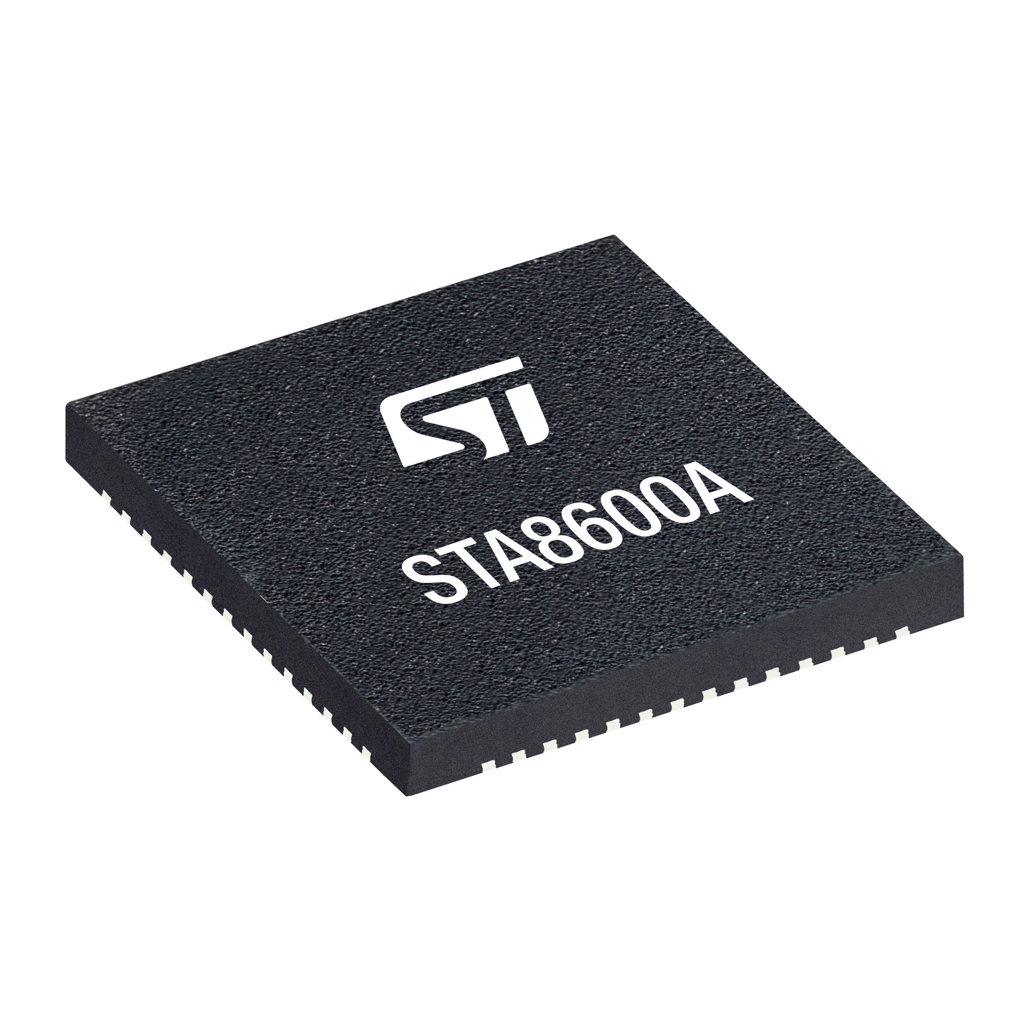 TeseoVI (STA8600A) in a VFQFPN package
Most GNSS receivers for automotive feature multiple dies in one package. There’s the digital microcontroller, a baseband radio, and sometimes a third die for memory. The industry adopted this approach because it bypassed significant manufacturing challenges that come from putting everything on the same die. Moreover, adding enough memory can also lead to a big die size, lowering yields and making devices more expensive. Using multiple dies also makes optimizing the RF easier, which leads to greater precision. Single-die GNSS receivers are typical in smartphones and much smaller systems that don’t require as much accuracy but have remained a problem for cars.
How did TeseoVI overcome this challenge?That’s why the TeseoVI is special. It brings the convenience and cost-effectiveness of the single-die approach that’s so popular on smartphones while overcoming the precision and reliability challenges that prevented such an approach from serving cars. To make this possible, ST optimized the RF and the phase-change memory (PCM), among other things. For the former, we employed a new generation of baseband processing, opening the door to new features (more on that later).
TeseoVI: Jamming protection What are the L1 and L5 signal bands?One of the features brought on by the new baseband processor is the ability to track L1 and L5 signals independently. L1 is the oldest GNSS signal, using a frequency of 1575.2 MHz. It’s the slowest and doesn’t travel well through obstacles, but its maturity means it is a preferred signal for most satellite positioning applications. L5 uses the 1176 MHz frequency and is the most advanced GNSS signal. Launched in 2021, it targets critical applications, like aviation, but is also available for consumer systems. It offers greater bandwidth thanks to higher power levels, improved accuracy thanks to interference rejection, and better robustness. Indeed, thanks to its lower frequency, it features a longer wavelength that deals better with obstacles.
How to jam the L1 signal?Another reason supporting L1 and L5 signals independently is essential is because it provides anti-jamming protection. Jamming happens when a signal overwhelms the receiver. It can result from unintentional electromagnetic interference from antennas or large infrastructure emitting intense radiation. There are also dedicated jammers to bypass fleet monitoring, insurance trackers, and more. The L1 frequency is very easy to jam. It doesn’t have redundancy features, and its low signal strength is easy to overwhelm, which causes the GNSS receiver to lose its lock on the signal, thus failing to acquire navigation data. It’s so easy that L1 jammers, although illegal in most countries, may cost less than US$20, according to The Resilient Navigation and Timing Foundation.
TeseoVI and anti-jammingInterestingly, even GNSS receivers that track L5 signals may require the L1 signal. Indeed, many devices acquire timing data from the L1 signal during their boot sequence and then use it to lock onto the L5 signal. The problem is that even a low-cost jammer could prevent a device from acquiring data from the L1 signal, meaning the receiver can’t use the L5 band. The new baseband processing in the TeseoVI introduced an L5-only mode, meaning it doesn’t need L1 to acquire data on L5. Consequently, it can bypass jammers. Additionally, L5 is so robust some estimate it to be 30 times harder to jam than L1.
TeseoVI: Spoofing protection How to spoof a GNSS signal?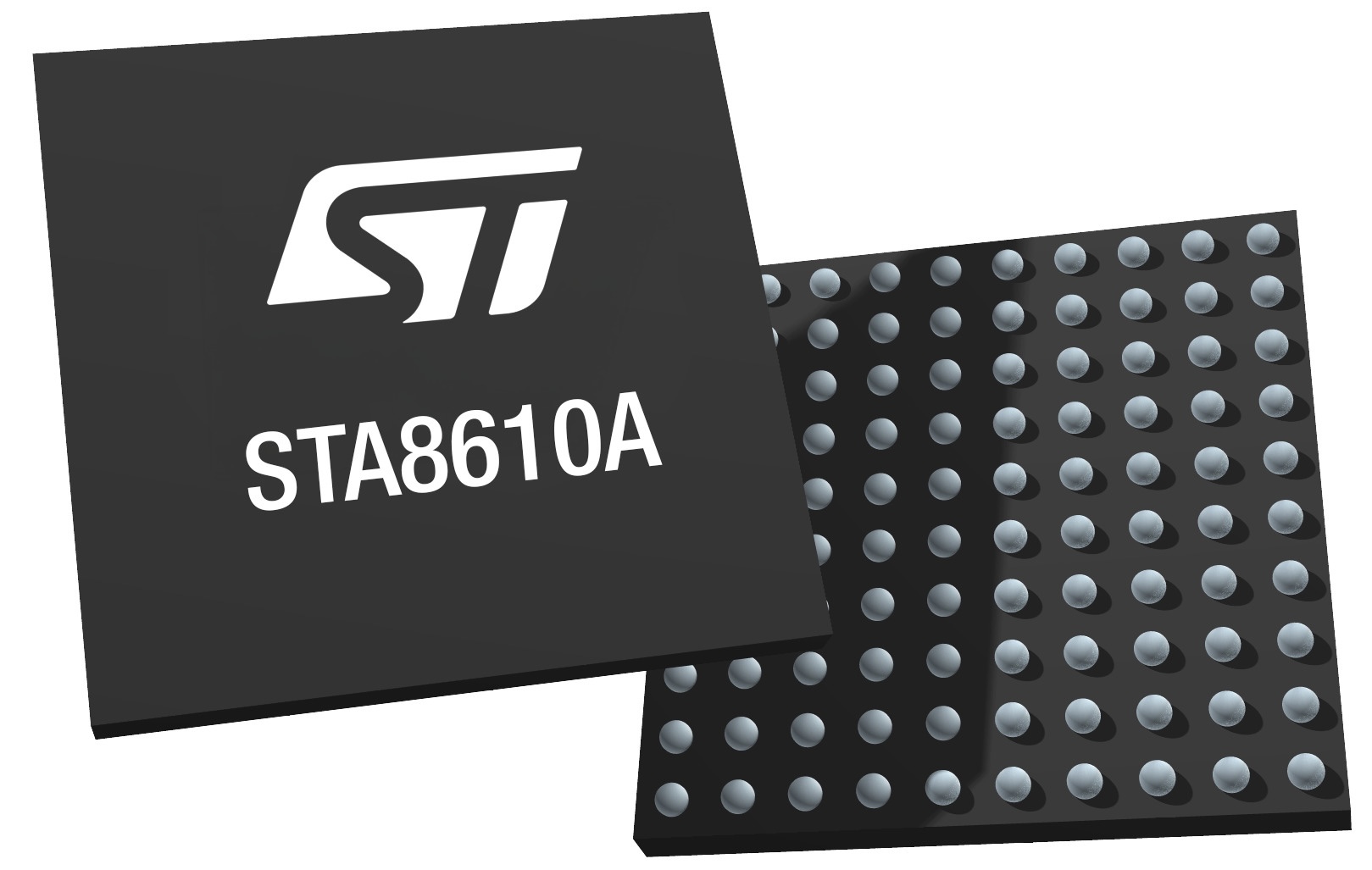 TeseoVI+ (STA8610A)
The new TeseoVI also supports the open service navigation message authentication (OSNMA) from the Galileo constellation. In a nutshell, the feature prevents spoofing attacks by cryptographically authenticating the source of a message. Very simply, the technology uses a message authentication code (MAC) to guarantee the authenticity of a signal’s provenance. It doesn’t encrypt the whole message but sends a series of codes, which is a far more efficient use of the bandwidth. Consequently, since Galileo generates the code, hackers can’t fake it. Additionally, since the standard sends multiple codes over time, hackers can’t just grab one key and reuse it in a replay attack. By the time they do so, the key has expired.
How to support OSNMA?To support OSNMA, hardware manufacturers must update their firmware and their software stack and offer enough processing power to handle the extra computations. This is why ST also provides extensive software implementations with its GNSS receivers. We know that taking advantage of new features can be complex. In this instance, decoding the OSNMA fields and managing the keys requires complex libraries that must pass audits and receive regular updates. Hence, the TeseoVI not only supports this anti-spoofing technology but enables developers to take advantage of it in their applications rapidly.
Making multiband more accessible More advanced features to mainstream cars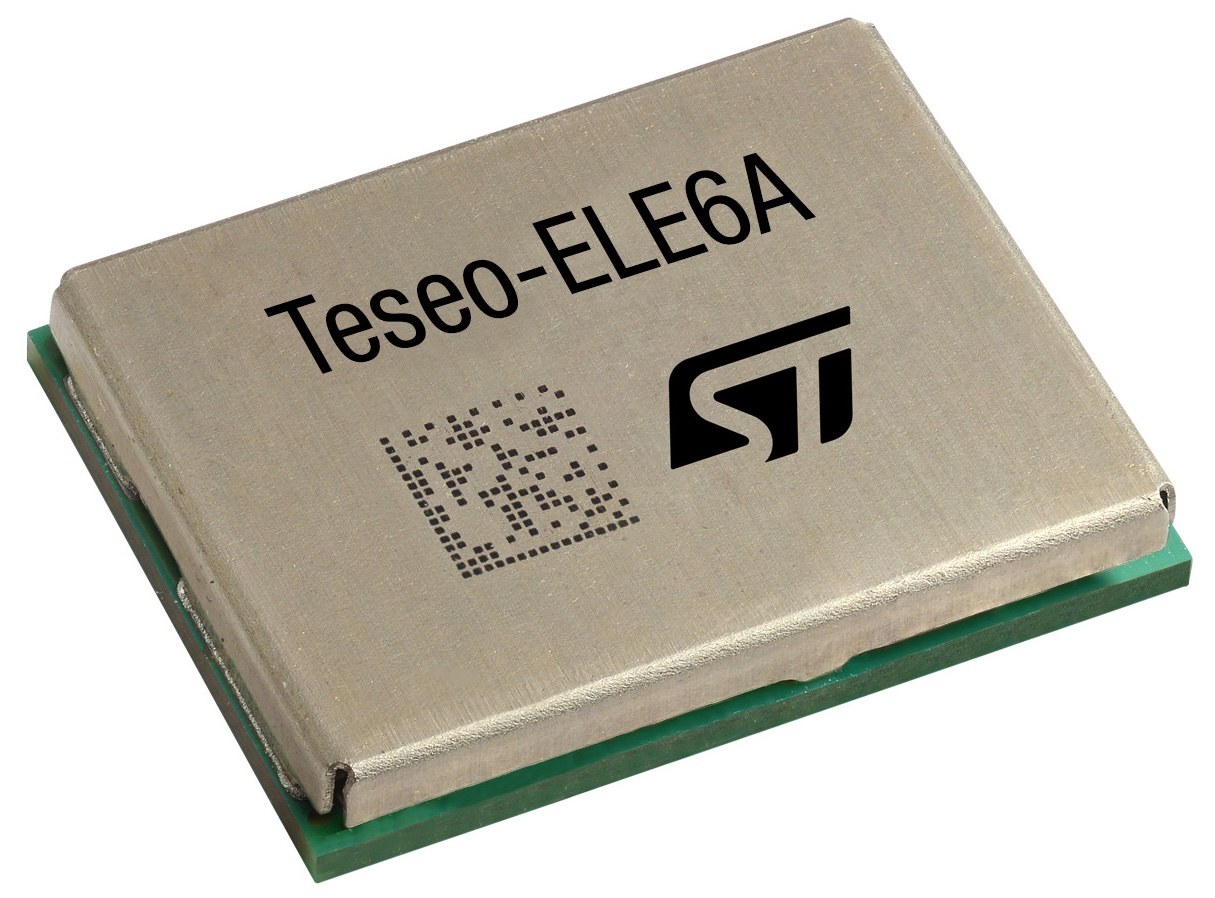 Teseo-ELE6A
One of the greatest benefits of a single-die design is the ability to lower the cost of materials. In fact, since there’s no need for external RF and external memory, engineers may target a BOM cost of about a dollar. Obviously, this is only a general reference point. In practice, the price will vary based on the complexity of the design and volumes. However, in all cases, it means that previous customers who used to avoid multiband solutions because they were too expensive will now be able to jump on the bandwagon. For instance, we can expect level 2 and 3 autonomous driving features to reach more mainstream vehicles.
More flexibility to integrators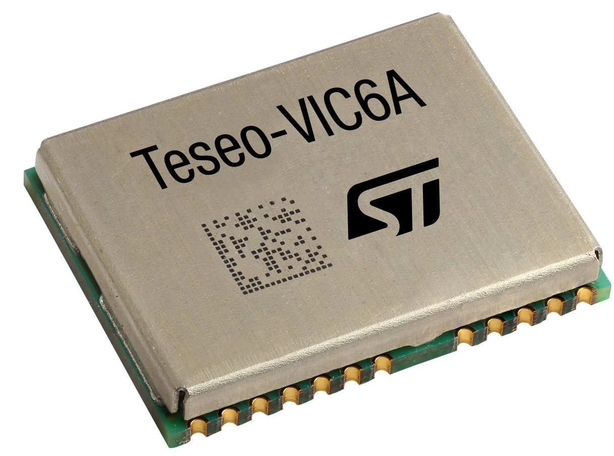 Teseo-VIC6A
The TeseoVI is also the first GNSS receiver for automotives to have a pin-to-pin compatible version for safety applications, the TeseoAPP2 (STA9200MA), which features the same QFN56 package as the TeseoVI (STA8600A). As a result, developers can simply create one reference design and switch between the ASIL-certified and the non-certified part number, depending on their needs.
ST will also be offering the TeseoVI+ (STA8610A). It’s the same device as the TeseoVI, but the TeseoVI+ can welcome custom algorithms thanks to dual M7 Core Processing and External Memory Interface (Flash/RAM). Hence, teams wanting to use their application can do away with our positioning and measurement software. Finally, we also offer a module with a 6-axis inertial sensor, the Teseo-VIC6A, and its safety alter ego, the Teseo-ELE6A.
The post TeseoVI: ST’s 1st single-die quad-band GNSS receiver makes autonomous driving mainstream appeared first on ELE Times.
Renesas Partners with Indian Government to Drive Innovation Through Startups and Industry-Academia Collaboration, Strengthening India’s Semiconductor Ecosystem
MOUs Signed with Indian Government and Inauguration of Renesas’ Bengaluru and Noida Offices Mark Investments to Accelerate Growth in India’s Key Semiconductor Hubs
Renesas Electronics Corporation announced its partnership with the Ministry of Electronics & Information Technology (MeitY), Government of India, to support local startups and academic institutions in the field of VLSI and embedded semiconductor systems. Renesas also celebrated the expansion of its offices in Bengaluru and Noida to accommodate its growing R&D teams, with the inauguration ceremonies. This strategic move underscores Renesas’ commitment to innovation and excellence in India and aims to drive continued growth in the region.
Renesas and the Centre for Development of Advanced Computing, an autonomous scientific society of MeitY, today signed and exchanged two Memoranda of Understanding (MOUs) under the MeitY Chips to Startup. These MOUs focus on 1) Supporting local startups by enabling them to drive technological advancement and promote local manufacturing in alignment with the Make in India initiative; and 2) Enhancing industry-academia collaboration by fostering an innovative, product-focused mindset among students.
India is a key market for Renesas, offering significant growth potential and access to a highly skilled talent pool. Recent collaborations include the OSAT factory project with CG power and Stars Microelectronics in Gujarat and the MOU with IIT Hyderabad. Renesas is also expanding its operations in India, with plans to increase its headcount to 1,000 by the end of 2025. This growth initiative reinforces Renesas’ long-term commitment to India and supports its ambition to become an employer of choice in this dynamic and fast-evolving market.
“The inauguration of our expanded offices marks a significant milestone for Renesas in India. It reflects our unwavering commitment to innovation, excellence, and the nurturing of local talent. By building products in India, for India and the world, we continue to drive growth and deliver meaningful impact across the Indian market,” said Malini Narayanamoorthi, India Country Manager and VP, MID Engineering, Analog & Connectivity Group at Renesas. “We are proud to sign two MOUs under the MeitY C2S programme, focused on advancing research, fostering innovation, and nurturing product-focused engineers. These strategic collaborations align with the Make in India initiative, aiming to strengthen local design and manufacturing capabilities and empower homegrown talent to drive the future of industry.”
MOUs under MeitY C2S programme
Renesas and C-DAC signed two MOUs to collaborate in the field of VLSI and embedded semiconductor systems, with the aim of supporting local startups and academic institutions to accelerate innovation and foster self-reliance in India’s semiconductor and product ecosystem. The C2S programme encompasses collaboration with over 250 academic institutions and R&D organizations across the country, including IITs, NITs, IIITs, government and private colleges, along with approximately 15 startups, creating a strong ecosystem for indigenous innovation.
- MOU for Startups: Renesas will help strengthen the product engineering capabilities of local startups by providing Renesas development boards and Altium Designer,the leading PCB design software.
- MOU for Academic Institutions: Renesas will support experiential learning by offering development boards, PCB education and training, Altium Designer software, and access to the Altium 365 cloud platform, aiming to empower the next generation of electronics engineers and nurture a community of innovators.
The post Renesas Partners with Indian Government to Drive Innovation Through Startups and Industry-Academia Collaboration, Strengthening India’s Semiconductor Ecosystem appeared first on ELE Times.
PSOC 4100T Plus microcontroller offers advanced sensing capabilities and system control in a single chip
Infineon Technologies AG introduces PSOC 4100T Plus, an Arm Cortex-M0+ microcontroller (MCU) with Multi-Sense. The new microcontroller offers a rich blend of analog and digital capabilities, featuring 128K Flash, 32K SRAM, and Infineon’s high-performance Multi-Sense technology, which includes CAPSENSE, inductive sensing and liquid level sensing. PSOC 4100T Plus also boasts enhanced reliability and is equipped with a range of enhancements and advanced sensing capabilities to form a complete solution for system control and human-machine interface applications.
“Infineon is committed to delivering best-in-class system control and HMI solutions with enhanced reliability,” says Vibheesh Bharathan, Director and Project Lead for PSOC 4 Multi-Sense from Infineon. “Our Multi-Sense capability represents a paradigm shift, driving next-generation sensing solutions for HMI and system control use cases. In this way, we are enabling the digitalization solutions of tomorrow for consumer and industrial applications.”
PSOC 4100T Plus can be used as a standalone general-purpose microcontroller, providing a robust platform for system control and management OR it can be utilized as a specialized HMI MCU, enabling the creation of intuitive and interactive interfaces. Alternatively, PSOC 4100T Plus can serve a single chip solution for both system control and touch HMI.
In its HMI MCU configuration, the device supports a range of sensing applications, including capacitive sensing for detecting user touch or proximity, inductive sensing for enabling touch over metallic surfaces, Machine Learning based liquid level sensing for monitoring liquid presence or levels, and CAPSENSE-based hover touch for detecting finger touch through a large airgap, making it a powerful tool for creating innovative and user-friendly interfaces.
PSOC 4100T Plus is a versatile and powerful platform designed to support a broad range of applications. For example:
Home appliances: Reliability is the top priority for home appliances. The PSOC 4100T Plus series addresses this critical requirement with significant enhancements, including 6500 V best-in-class electrostatic discharge protection and a 1% internal main oscillator accuracy. In addition, the advanced HMI features, such as hover touch, provide a solution to several design challenges, including the need for simplified and cost-effective stack up, touch operation through airgap. With the combination of complementary sensing technologies of Multi-Sense, designers can effectively address the design challenges they face.
Consumer electronics: PSOC 4100T Plus series elevates the human-machine interface capabilities in consumer electronics by providing a compact and efficient solution for sensor designs. Leveraging its 5th Generation CAPSENSE technology, the PSOC 4100T Plus offers high signal-to-noise ratio and low power consumption. Additionally, its waterproof design enables the device to operate reliably in harsh environments, including outdoor applications.
Touchpad and touchscreen applications: PSOC 4100T Plus series offers a high resolution 2D finger tracking user interface, enabling the creation touchpads and touchscreens. With 32 sensor inputs, the device can be configured to support up to 256 nodes, allowing for a wide range of design possibilities. For example, a touchpad can be designed with an 80mm x 80mm surface area with a 5mm diamond pitch, resulting in a high-resolution multi-finger tracking. Similarly, a 4-inch touchscreen can be driven by PSOC 4100T Plus for multi-finger use. Both touchpad and touchscreen user interfaces supported with built-in, configurable gesture engine.
To support the development of multi-sense applications, a comprehensive suite of software tools and resources are offered. The CAPSENSE Tuner allows designers to easily configure and optimize capacitive sensing applications, while the Inductive Sensing Design Guide and Liquid Level Sensing Design Guide provide detailed guidance on implementing these technologies. Additionally, the ML-based liquid level sensing model trainer enables developers to overcome challenges like manufacturing variations, varying airgaps with removable tanks.
The post PSOC 4100T Plus microcontroller offers advanced sensing capabilities and system control in a single chip appeared first on ELE Times.
Infineon introduces CoolGaN Bidirectional Switch 650 V G5 for enhanced efficiency and reliability in power systems
Infineon Technologies AG is introducing the CoolGaN Bidirectional Switch 650 V G5, a gallium nitride (GaN) switch capable of actively blocking voltage and current in both directions. Featuring a common-drain design and a double-gate structure, it leverages Infineon’s robust gate injection transistor technology to deliver a monolithic bidirectional switch, enabled by Infineon’s CoolGaN technology. The device serves as a highly efficient replacement for traditional back-to-back configurations commonly used in converters.
The bidirectional CoolGaN switch offers several key advantages for power conversion systems. By integrating two switches in a single device, it simplifies the design of cycloconverter topologies, enabling single-stage power conversion, eliminating the need for multiple conversion stages. This leads to improved efficiency, increased reliability, and a more compact design. BDS-based microinverters also benefit from higher power density and reduced component count, which simplifies manufacturing and reduces costs. Additionally, the device supports advanced grid functions such as reactive power compensation and bidirectional operation.
As a result, this solution holds significant potential across a wide range of applications, including:
Microinverters: The CoolGaN bidirectional switch enables simpler and more efficient microinverter designs, reducing both size and cost. This makes microinverters more attractive for residential and commercial solar installations.
Energy Storage Systems (ESS): In ESS applications such as battery chargers and dischargers, the switch allows for more efficient and reliable energy storage and release.
Electric Vehicle (EV) Charging: In EV charging systems, the BDS switch supports faster, more efficient charging while also enabling vehicle-to-grid functionality, where energy stored in the vehicle battery can be fed back into the grid.
Motor control: The CoolGaN BDS is ideal for use in Current Source Inverters for industrial motor drives. Compared to traditional Voltage Source Inverters, CSIs offer benefits such as:
- Producing a sinusoidal output voltage, which supports longer cable runs, reduced losses, and improved fault tolerance.
- Replacing the DC-link capacitor with an inductor, improving high-temperature performance and short-circuit protection.
- Higher efficiency at partial loads, lower EMI, inherent buck-boost capability for voltage variation, and scalability for parallel operation.
These features make CSIs a more robust and efficient alternative for industrial motor applications.
AI data centers: In AI server power supplies, bidirectional switches like CoolGaN support higher switching frequencies and power density in architectures such as Vienna rectifiers and H4 PFCs. A single CoolGaN BDS can replace two conventional switches, reducing component count, cost, size, and overall power losses.
The post Infineon introduces CoolGaN Bidirectional Switch 650 V G5 for enhanced efficiency and reliability in power systems appeared first on ELE Times.
Top 10 RAM Brands in India
Random Access Memory (RAM) is an essential part of any computing system, its speed and efficiency depending on it. India’s RAM market has seen strong growth over the past few years due to growing demand for high-end computing, gaming and enterprise applications. The Indian RAM market has both local and foreign players, providing a variety of RAM modules such as DDR3, DDR4, and DDR5 technologies. In India, there are quite a few brands that provide top-notch RAM modules for various purposes. Here’s a glimpse at the top 10 RAM brands in India, their origin and specifications.
- Corsair
Corsair is one of the first memory module makers based in the United States that primarily serves as a supplier for gamers, business users and PC enthusiasts, Its RAM is designed with aggressive cooling systems, customizable RGB color, and optimum speed for overlocking.
- Kingston
Kingston, an American company, specializes in the manufacturing of top-class memory solutions. It provides dependable RAM modules under various categories such as DDR3, DDR4, and DDR5, along with its HyperX line that caters to gamers and high-end users.
- Samsung
Samsung, headquartered in South Korea, is a world leader in semiconductor technology and producers top-notch RAM modules. Their memory solutions offer superior speed and efficiency and are in great demand for use in laptops, desktops and workstations. The company manufactures memory solutions over a range of generations, such as DDR3, DDR4 and DDR5, which find applications in various devices, from laptops and desktops to enterprise servers.
- G. SKILL
Based in Taiwan, G. SKILL is a leader in gaming memory solutions, offering ultra-high -speed frequencies and leading cooling technology. Their Trident Z series RAM modules are especially well-linked among gaming enthusiasts searching for extreme overlocking capabilities.
- Crucial
A Micron subsidiary, Crucial is U.S. based and offers reliable and cost-effective RAM solutions. Its Ballistix series popularized, Crucial RAM has widespread use for general computing while being both performant and price -effective.
- ADATA
Taiwanese by origin, ADATA produces high-speed RAM modules featuring innovative designs. ADATA produces DDR4 and DDR5 memory solutions, with the XPG gaming series being specifically designed for gamers looking for top-class performance and longevity.
- Transcend
Another Taiwanese company, Transcend is known for making industrial-grade memory modules. RAM solutions by Transcend are designed for long-lasting durability and can be used in commercial and consumer applications.
- SK Hynix
Headquartered in South Korea, SK Hynix is an expert in enterprise-level memory solutions. Their RAM products guarantee high-speed performance, reliability and peak efficiency, serving professional and industrial computing purposes.
- Patriot
Patriot, an American company, specializes in providing high-performance RAM solutions with superior heat dissipation technology. Their Viper gaming line is designed for gaming systems that need fast and stable memory.
10. TeamGroup
Located in Taiwan, TeamGroup specializes in manufacturing stylish and high-performance RAM modules. Their T-Force gaming line offers a blend of appearance and superior cooling technology, and hence it is a top pick for users who are into performance.
|
Brand Name |
Example Model |
Key Specifications |
|
Corsair |
Corsair Vengeance RGB Pro | DDR4, DDR5, RGB options, High-speed modules |
|
Kingston |
Kingston Fury Beast |
DDR3, DDR4, DDR5, Value and HyperX series |
|
G. SKILL |
G. SKILL Trident Z RGB |
DDR4, DDR5, High-frequency modules, RGB lighting |
|
Crucial |
Crucial Ballistix |
DDR3, DDR4, DDR5, Low-cost alternatives |
|
ADATA |
ADATA XPG Spectrix D60G |
DDR3, DDR4. DDR5, XPG Gaming series |
|
Transcend |
Transcend Jet Ram |
DDR3, DDR4, DDR5, Industrial-grade memory |
|
Samsung |
Samsung DDR4-3200 |
DDR3, DDR4, DDR5, High-capacity modules |
|
Hynix |
SK Hynix Gold P31 |
DDR3, DDR4, DDR5, Enterprise-grade memory |
|
Patriot |
Patriot Viper Steel |
DDR4, DDR5, Viper gaming series |
| TeamGroup | TeamGroup T-Force Delta |
RGB, DDR4, DDR5, T-Force gaming series |
There is competition among brands in the varied Indian RAM market to offer dependable, fast memory solutions for a range of computing requirements. While Transcend, ADATA, and Crucial provide good mid-range options, Corsair, Kingston, and G. SKILL stand out as premium options for gaming and high-performance applications. With their commitment to quality and innovation, Samsung and Hynix remain formidable competitors in the semiconductor sector.
The post Top 10 RAM Brands in India appeared first on ELE Times.
Infineon and Visteon Collaborate on Advanced Power Conversion Systems for Next-Generation Electric Vehicles
Infineon Technologies AG, the leading provider of automotive semiconductors, and Visteon Corporation, a global leader in automotive cockpit electronics, announced the companies have signed a Memorandum of Understanding to advance the development of next-generation electric vehicle powertrains.
In this joint effort, Infineon and Visteon will collaborate and integrate power conversion devices based on Infineon semiconductors, with particular emphasis on wideband gap device technologies, which provide significant advantages in power conversion applications compared to silicon-based semiconductors. These devices include greater power density, efficiency and thermal performance, which contribute to improved efficiency and reduced system costs for next-generation power conversion modules for the automotive sector.
Future Visteon EV powertrain applications incorporating Infineon CoolGaN (Gallium Nitride) and CoolSiC (Silicon Carbide) devices may include battery junction boxes, DC-DC converters and on-board chargers. The resulting powertrain systems will conform to the highest efficiency, robustness and reliability.
“Working with Infineon allows us to integrate cutting-edge semiconductor technologies that are essential in improving power conversion efficiency and overall system capability of next generation electric vehicles,” said Dr. Tao Wang, Head of the Electrification Product Line of Visteon Corporation. “This collaboration will advance technologies that accelerate the transition to a more sustainable and efficient mobility ecosystem.”
“Visteon is a recognized innovator and an early adopter of new technologies, making them an ideal partner for us,” said Peter Schaefer, Chief Sales Officer Automotive, Infineon Technologies AG. “Together, we will push the boundaries of electric vehicle technology and provide superior solutions to the global automotive industry.”
The post Infineon and Visteon Collaborate on Advanced Power Conversion Systems for Next-Generation Electric Vehicles appeared first on ELE Times.
Pages

